Bipolar Junction Transistor
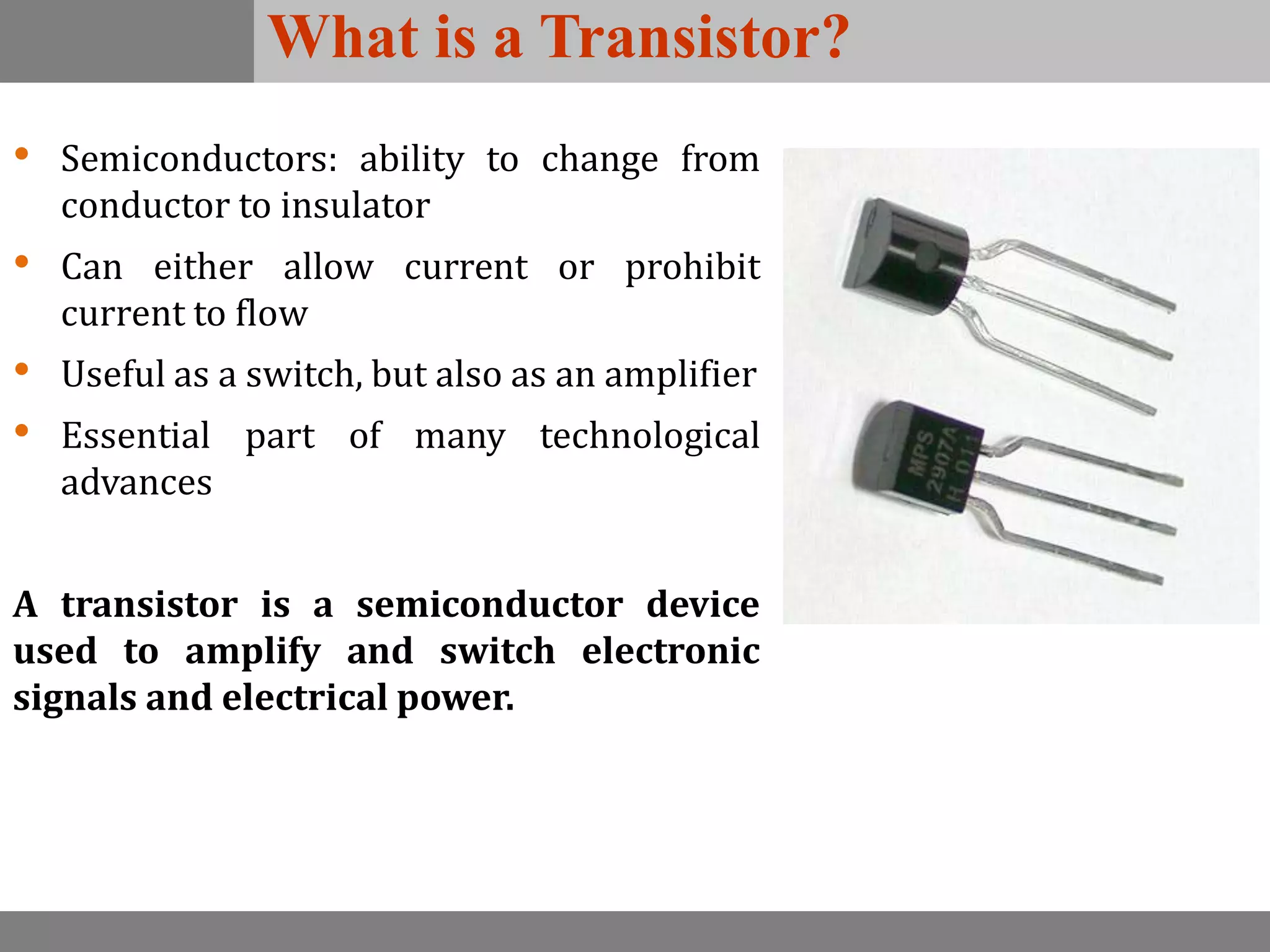
What is a Transistor?
• Semiconductors: ability to change from
conductor to insulator
• Can either allow current or prohibit
current to flow
• Useful as a switch, but also as an amplifier
• Essential part of many technological
advances
A transistor is a semiconductor device
used to amplify and switch electronic
signals and electrical power.
Transistor Operation
With the external sources, VEE and VCC, connected as shown:
• The emitter-base junction is forward biased
• The base-collector junction is reverse biased
3
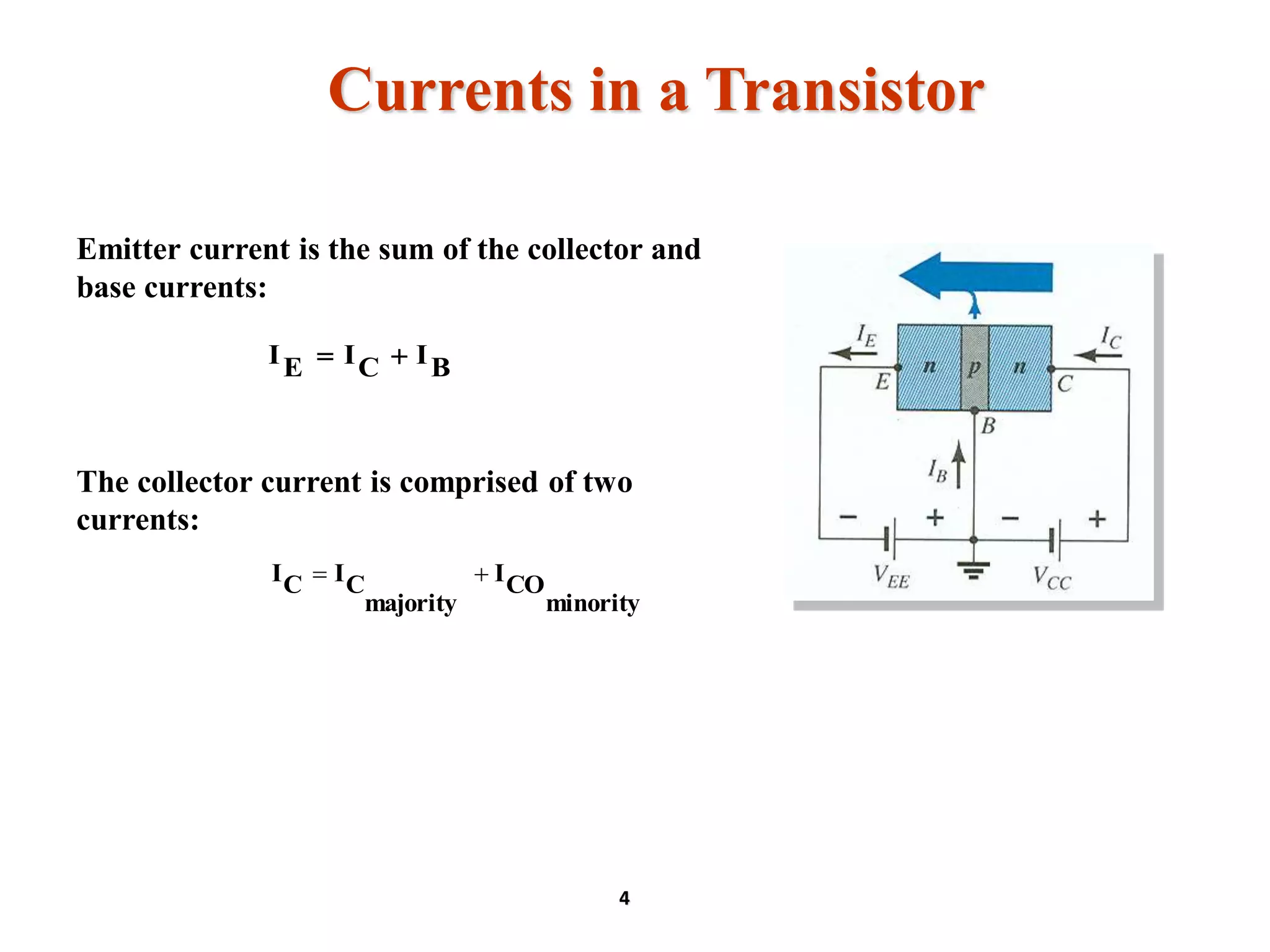
Currents in a Transistor
The collector current is comprised of two
currents:
BICIEI 
minority
COI
majority
CICI 
Emitter current is the sum of the collector and
base currents:
4
Transistor
SYMBOLS(BJTS)
Bipolar Junction Transistor
• A single p-n junction has two different types of bias:
- Forward Bias
- Reverse Bias
• Thus, a two pn-jnuction device has four types of bias.
SaturationForwardForward
ActiveForwardReverse
Cut-offReverseForward
Cut-offReverseReverse
Mode of operationBE junction
(BEJ)
BC junction
(BCJ)
8
Transistor Operation
BJT Construction
• The emitter layer is heavily doped, the base lightly
doped and collector only lightly doped.
• The doping of the sandwiched layer is considerably less
than the outer layers (typically 10:1 or less).
• Lower doping level decreases the conductivity of the
material by limiting the number of free electrons.
• The outer layers have widths much greater than the
sandwiched p- or n-type material. The ratio of the total
width to that of the central layer is 150:1.
JUNCTIONS
BASE-EMITTER JUNCTION(BEJ):
The pn junction joining the base region and the emitter region is
called the base-emitter junction
COLLECTOR-BASE JUNCTION(CBJ):
The pn junction joining the base region and the collector region
is called the collector-base junction
Transistor as Two Diodes
Transistor Currents(NPN)
𝐼 𝐸 = 𝐼 𝐶 + 𝐼 𝐵
Transistor Currents(PNP)
𝐼 𝐸 = 𝐼 𝐶 + 𝐼 𝐵
NPN
PNP
BJT Modes of Operation
MODE IB or VCE Char. BEJ CBJ
CutOff IB = Very small Reverse Reverse
Active VCE = Moderate Forward Reverse
Saturation VCE = Small Forward Forward
Cut-off –
The transistor is “Fully-OFF” operating as a switch. There is voltage, but little
current
Active Region –
The transistor operates as an amplifier
Saturation –
The transistor is “Fully-ON” operating as a switch. There is current, but little
voltage.
DC BIAS VOLTAGES
When a transistor is connected to dc bias voltages, for both npn and
pnp types,
VBB forward-biases the base-emitter junction
VCC reverse-biases the base-collector junction
DC Beta ( β )
𝑰 𝑬 = 𝑰 𝑪 + 𝑰 𝑩
The dc current gain of a transistor is the ratio of the dc collector
current (𝐼 𝐶) to the dc base current (𝐼 𝐵)
𝜷 =
𝑰 𝑪
𝑰 𝑩
𝑰 𝑪 = 𝜷𝑰 𝑩
DC Alpha ( α )
𝑰 𝑬 = 𝑰 𝑪 + 𝑰 𝑩
The ratio of the dc collector current (𝐼 𝐶) to the dc emitter current
(𝐼 𝐸) is the dc alpha (αDC).
𝜶 =
𝑰 𝑪
𝑰 𝑬
𝑰 𝑪 = 𝜶𝑰 𝑬
BJT Current–Voltage Relationships
𝑰 𝑬 = 𝑰 𝑪 + 𝑰 𝑩
𝑰 𝑪 = 𝑰 𝑬 − 𝑰 𝑩
𝑰 𝑩 = 𝑰 𝑬 − 𝑰 𝑪
𝜶 =
𝜷
𝜷 + 𝟏
𝜷 =
𝜶
𝟏 − 𝜶
𝜷 =
𝑰 𝑪
𝑰 𝑩
, 𝑰 𝑪 = 𝜷𝑰 𝑩
𝜶 =
𝑰 𝑪
𝑰 𝑬
, 𝑰 𝑪 = 𝜶𝑰 𝑬
𝑰 𝑬 = 𝑰 𝑪 + 𝑰 𝑩
𝑰 𝑬 = 𝜷𝑰 𝑩 + 𝑰 𝑩
𝑰 𝑬 = 𝜷 + 𝟏 𝑰 𝑩
𝑰 𝑬 = 𝑰 𝑪 + 𝑰 𝑩
𝑰 𝑬 = 𝜶𝑰 𝑬 + 𝑰 𝑩
𝑰 𝑩 = (𝟏 − 𝜶)𝑰 𝑬
Modes of Operation(NPN)
BJT configurations
1. Common Emitter Configuration –
has both Current and Voltage Gain.
2. Common Base Configuration –
has Voltage Gain but no Current Gain.
3. Common Collector Configuration –
has Current Gain but no Voltage Gain.
Common-Base Configuration
The base is common to both input (emitter–base) and
output (collector–base) of the transistor.
23
Common Base Configuration
Common Base or grounded base configuration, the BASE connection
is common to both the input signal AND the output signal with the
input signal being applied between the base and the emitter
terminals. The corresponding output signal is taken from between
the base and the collector terminals
Input: Emitter
Output: Collector
Common-Base Amplifier
Input Characteristics
This curve shows the relationship
between of input current (IE) to input
voltage (VBE) for three output voltage
(VCB) levels.
25
This graph demonstrates
the output current (IC) to
an output voltage (VCB) for
various levels of input
current (IE).
Common-Base Amplifier
Output Characteristics
26
Operating Regions
• Active – Operating range of the
amplifier.
• Cutoff – The amplifier is basically
off. There is voltage, but little
current.
• Saturation – The amplifier is full on.
There is current, but little voltage.
27
E
I
C
I 
Silicon)(forV0.7BEV 
Approximations
Emitter and collector currents:
Base-emitter voltage:
28
Ideally: a = 1
In reality: a is between 0.9 and 0.998
Alpha (a)
Alpha (a) is the ratio of IC to IE :
EI
CI
α dc
Alpha (a) in the AC mode:
EI
CI
α
Δ
Δ
ac 
29
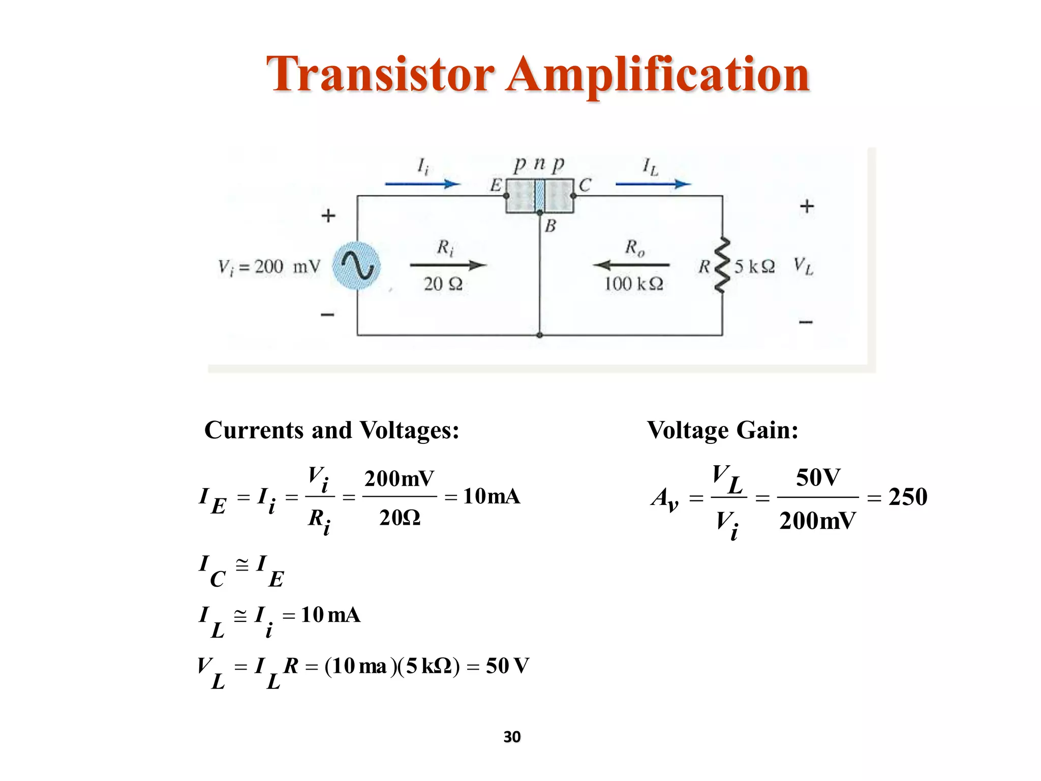
Transistor Amplification
Voltage Gain:
V50kΩ5ma10
mA10
10mA
20Ω
200mV




))((R
L
I
L
V
i
I
L
I
E
I
C
I
iR
iV
iIEI
Currents and Voltages:
30
250
200mV
50V

iV
LV
vA
Common–Emitter Configuration
The emitter is common to both input
(base-emitter) and output (collector-
emitter).
The input is on the base and the
output is on the collector.
31
Common Emitter Configuration
Common Emitter or grounded emitter configuration, the input
signal is applied between the base, while the output is taken from
between the collector and the emitter as shown.
Input: Base
Output: Collector
Common-Emitter Characteristics
Collector Characteristics Base Characteristics
33
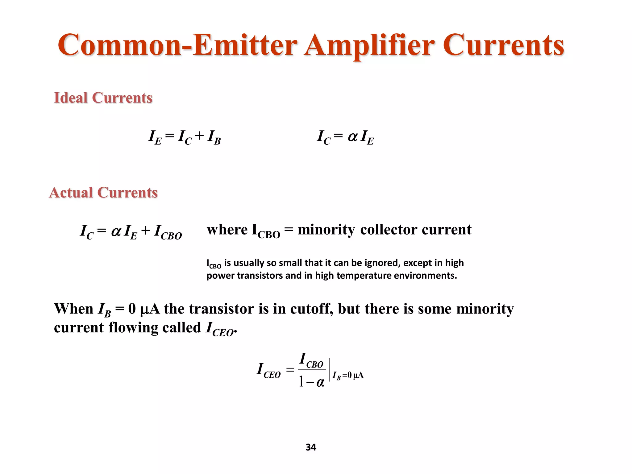
Common-Emitter Amplifier Currents
Ideal Currents
IE = IC + IB IC = a IE
Actual Currents
IC = a IE + ICBO
When IB = 0 A the transistor is in cutoff, but there is some minority
current flowing called ICEO.
μA0

 BI
CBO
CEO
α
I
I
1
where ICBO = minority collector current
34
ICBO is usually so small that it can be ignored, except in high
power transistors and in high temperature environments.
Beta ()
In DC mode:
In AC mode:
 represents the amplification factor of a transistor. ( is
sometimes referred to as hfe, a term used in transistor modeling
calculations)
B
C
I
I
β dc
constantac 


 CEV
B
C
I
I

35
Determining  from a Graph
Beta ()
108
A25
mA2.7
β 7.5VDC CE


 
100
μA10
mA1
μA)20μA(30
mA)2.2mA(3.2
β
7.5V
AC
CE






36
Relationship between amplification factors  and a
1β
β
α


1α
α
β


Beta ()
Relationship Between Currents
BC βII  BE 1)I(βI 
37
Common–Collector Configuration
The input is on the
base and the output is
on the emitter.
38
Common Collector Configuration
Common Collector or grounded collector configuration, the
collector is now common through the supply. The input signal is
connected directly to the base, while the output is taken from the
emitter load as shown. This type of configuration is commonly
known as a Voltage Follower or Emitter Follower circuit.
Input: Base
Output: Emitter
Common–Collector Configuration
The characteristics are
similar to those of the
common-emitter
configuration, except the
vertical axis is IE.
40
VCE is at maximum and IC is at
minimum (ICmax= ICEO) in the cutoff
region.
IC is at maximum and VCE is at
minimum (VCE max = VCEsat = VCEO) in
the saturation region.
The transistor operates in the active
region between saturation and cutoff.
Operating Limits for Each Configuration
41
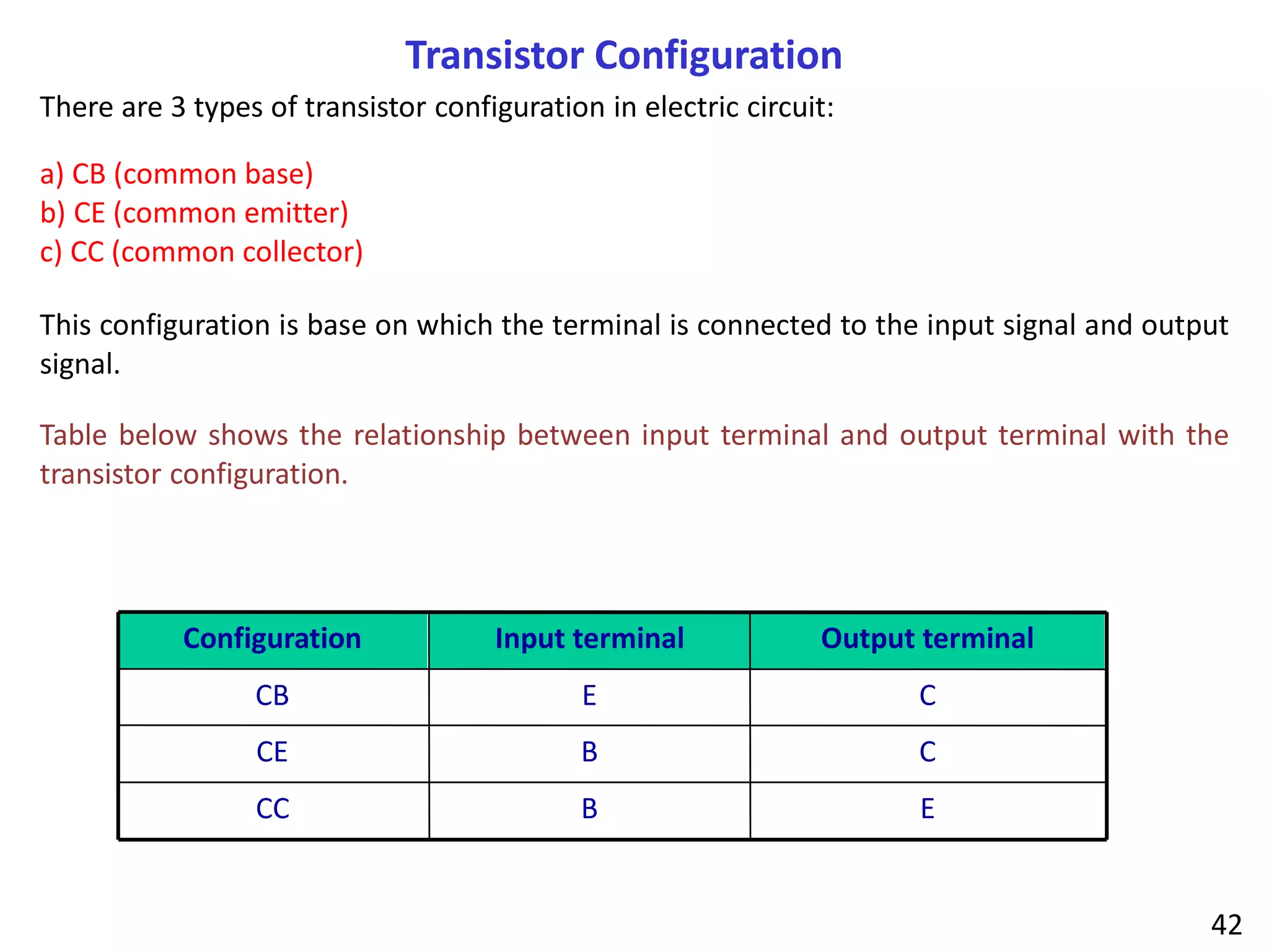
There are 3 types of transistor configuration in electric circuit:
a) CB (common base)
b) CE (common emitter)
c) CC (common collector)
This configuration is base on which the terminal is connected to the input signal and output
signal.
Table below shows the relationship between input terminal and output terminal with the
transistor configuration.
EBCC
CBCE
CECB
Output terminalInput terminalConfiguration
42
Transistor Configuration
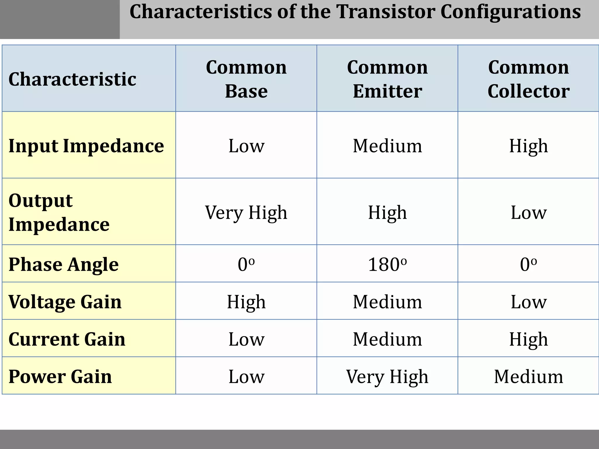
Characteristics of the Transistor Configurations
Characteristic
Common
Base
Common
Emitter
Common
Collector
Input Impedance Low Medium High
Output
Impedance
Very High High Low
Phase Angle 0o 180o 0o
Voltage Gain High Medium Low
Current Gain Low Medium High
Power Gain Low Very High Medium
Power Dissipation
Common-collector:
CCBCmax IVP 
CCECmax IVP 
ECECmax IVP 
Common-base:
Common-emitter:
44
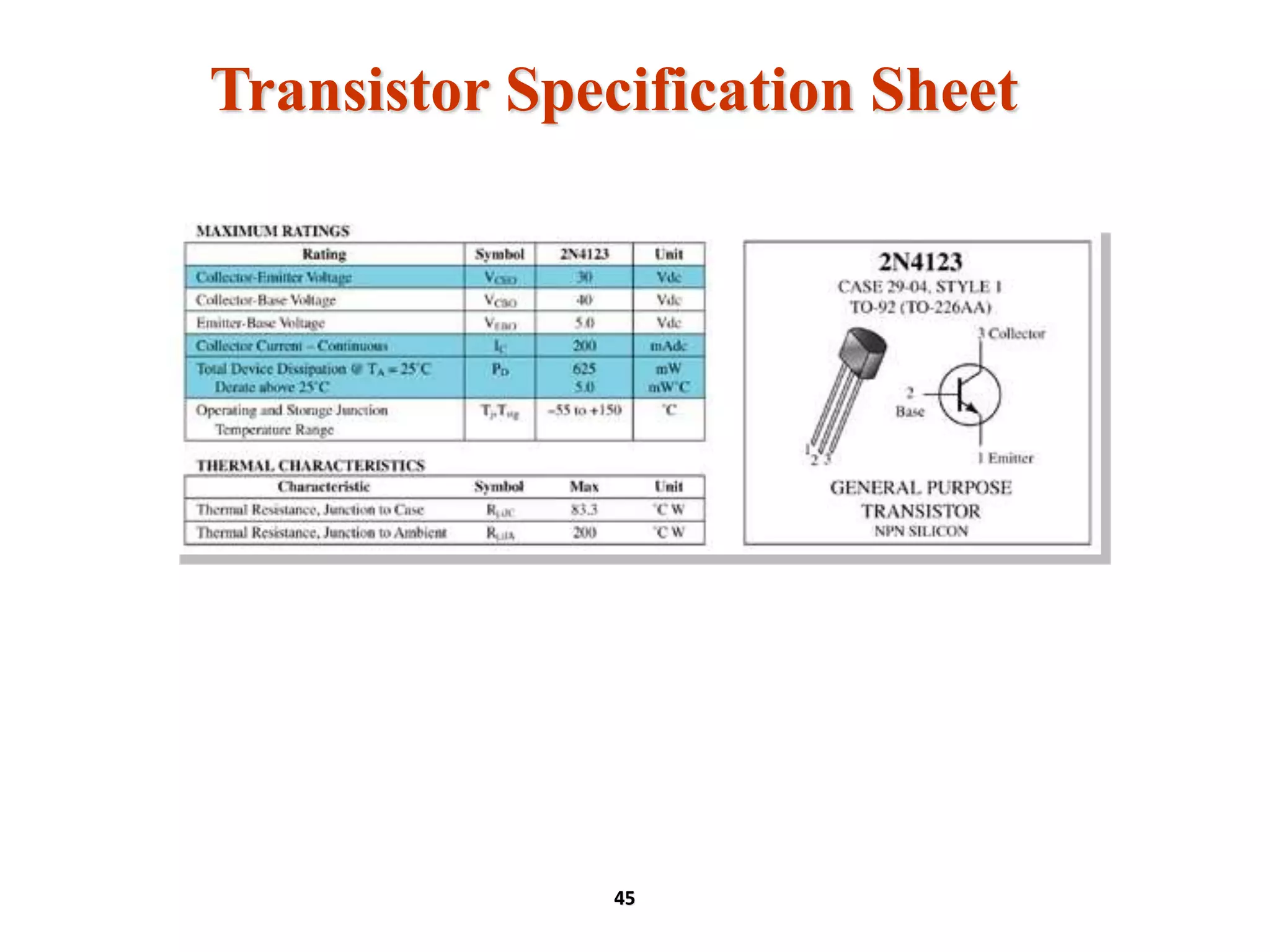
Transistor Specification Sheet
45
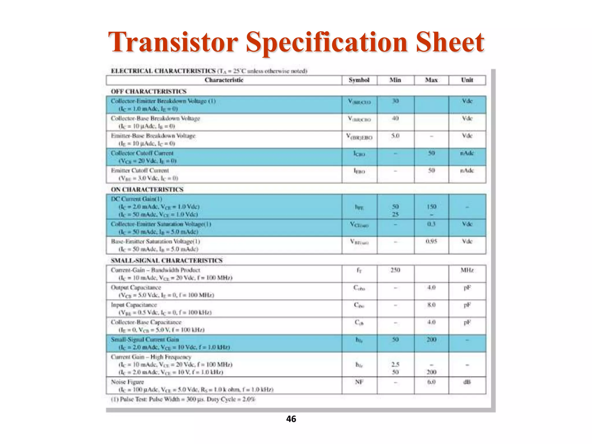
Transistor Specification Sheet
46
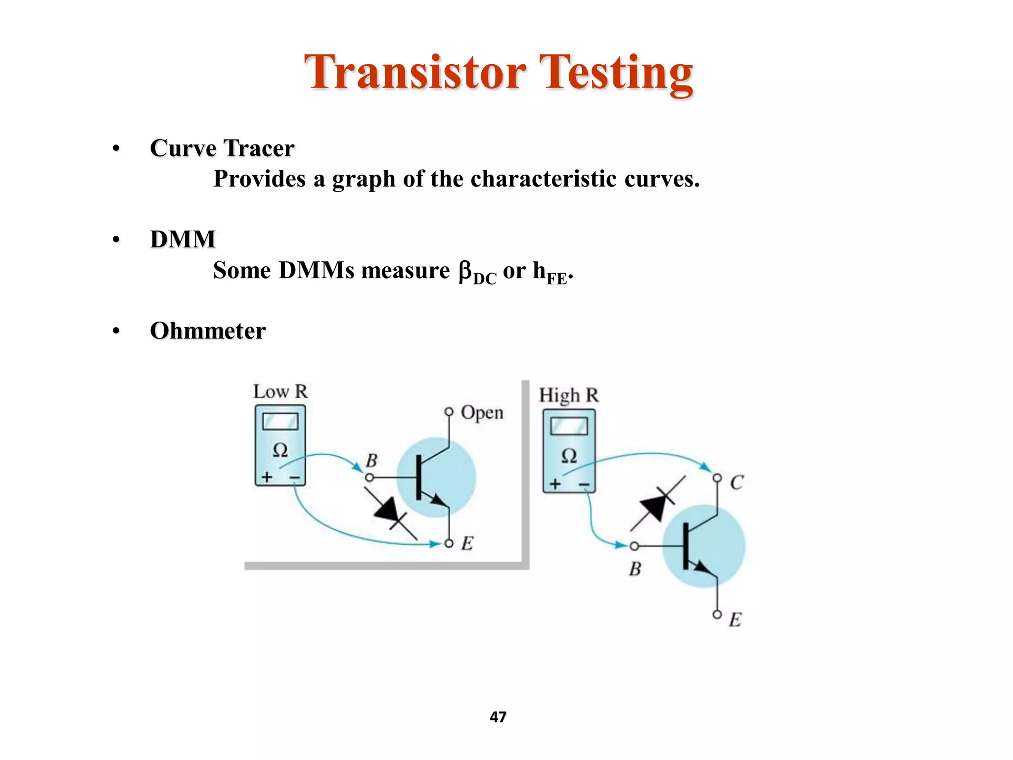
Transistor Testing
• Curve Tracer
Provides a graph of the characteristic curves.
• DMM
Some DMMs measure DC or hFE.
• Ohmmeter
47
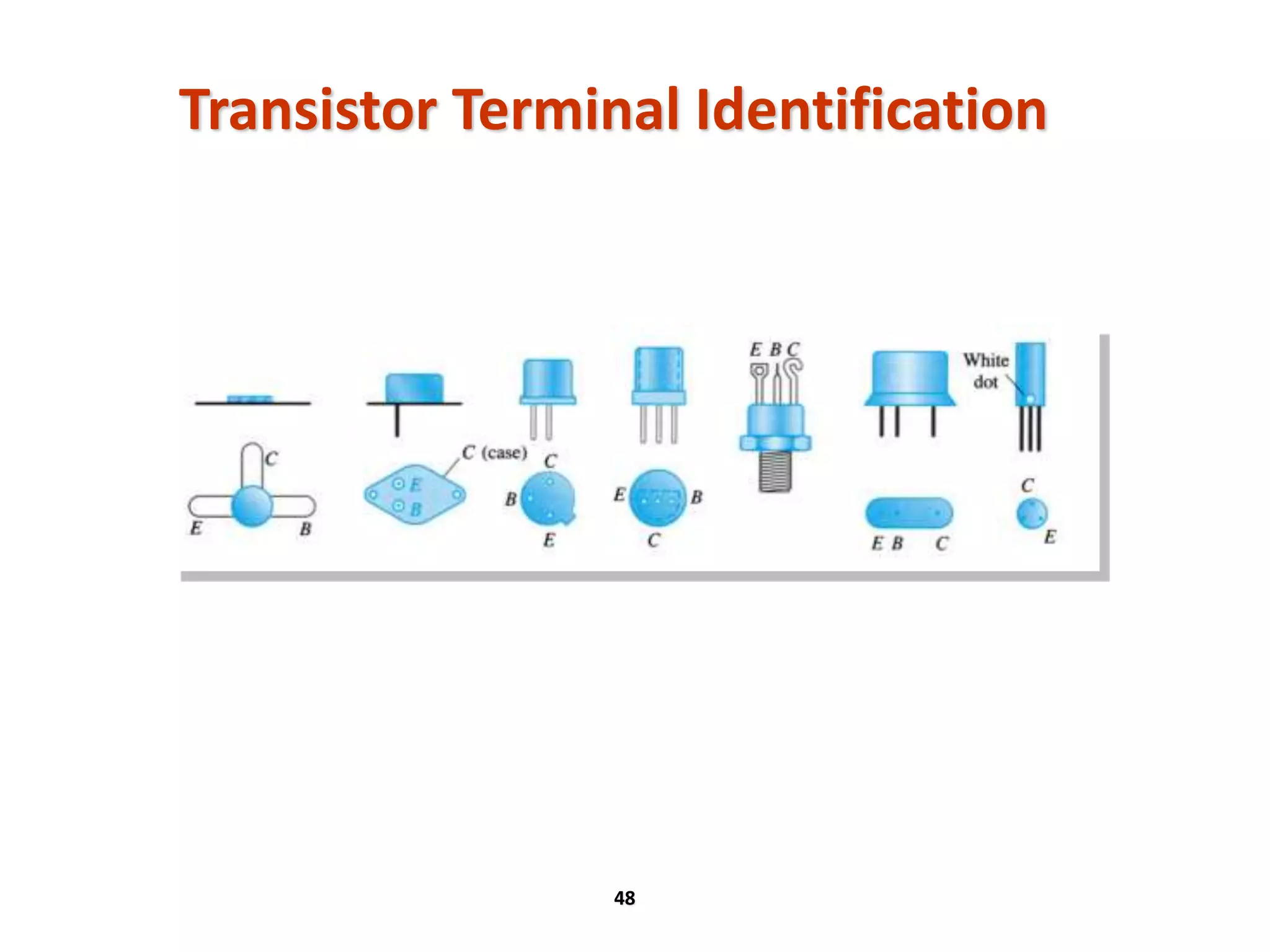
Transistor Terminal Identification
48

Electronics 1 : Chapter # 06 : Bipolar Junction Transistor

  • 1.
  • 2.
    What is aTransistor? • Semiconductors: ability to change from conductor to insulator • Can either allow current or prohibit current to flow • Useful as a switch, but also as an amplifier • Essential part of many technological advances A transistor is a semiconductor device used to amplify and switch electronic signals and electrical power.
  • 3.
    Transistor Operation With theexternal sources, VEE and VCC, connected as shown: • The emitter-base junction is forward biased • The base-collector junction is reverse biased 3
  • 4.
    Currents in aTransistor The collector current is comprised of two currents: BICIEI  minority COI majority CICI  Emitter current is the sum of the collector and base currents: 4
  • 5.
  • 6.
  • 7.
  • 8.
    • A singlep-n junction has two different types of bias: - Forward Bias - Reverse Bias • Thus, a two pn-jnuction device has four types of bias. SaturationForwardForward ActiveForwardReverse Cut-offReverseForward Cut-offReverseReverse Mode of operationBE junction (BEJ) BC junction (BCJ) 8 Transistor Operation
  • 9.
    BJT Construction • Theemitter layer is heavily doped, the base lightly doped and collector only lightly doped. • The doping of the sandwiched layer is considerably less than the outer layers (typically 10:1 or less). • Lower doping level decreases the conductivity of the material by limiting the number of free electrons. • The outer layers have widths much greater than the sandwiched p- or n-type material. The ratio of the total width to that of the central layer is 150:1.
  • 10.
    JUNCTIONS BASE-EMITTER JUNCTION(BEJ): The pnjunction joining the base region and the emitter region is called the base-emitter junction COLLECTOR-BASE JUNCTION(CBJ): The pn junction joining the base region and the collector region is called the collector-base junction
  • 11.
  • 12.
    Transistor Currents(NPN) 𝐼 𝐸= 𝐼 𝐶 + 𝐼 𝐵
  • 13.
    Transistor Currents(PNP) 𝐼 𝐸= 𝐼 𝐶 + 𝐼 𝐵
  • 14.
  • 15.
  • 16.
    BJT Modes ofOperation MODE IB or VCE Char. BEJ CBJ CutOff IB = Very small Reverse Reverse Active VCE = Moderate Forward Reverse Saturation VCE = Small Forward Forward Cut-off – The transistor is “Fully-OFF” operating as a switch. There is voltage, but little current Active Region – The transistor operates as an amplifier Saturation – The transistor is “Fully-ON” operating as a switch. There is current, but little voltage.
  • 17.
    DC BIAS VOLTAGES Whena transistor is connected to dc bias voltages, for both npn and pnp types, VBB forward-biases the base-emitter junction VCC reverse-biases the base-collector junction
  • 18.
    DC Beta (β ) 𝑰 𝑬 = 𝑰 𝑪 + 𝑰 𝑩 The dc current gain of a transistor is the ratio of the dc collector current (𝐼 𝐶) to the dc base current (𝐼 𝐵) 𝜷 = 𝑰 𝑪 𝑰 𝑩 𝑰 𝑪 = 𝜷𝑰 𝑩
  • 19.
    DC Alpha (α ) 𝑰 𝑬 = 𝑰 𝑪 + 𝑰 𝑩 The ratio of the dc collector current (𝐼 𝐶) to the dc emitter current (𝐼 𝐸) is the dc alpha (αDC). 𝜶 = 𝑰 𝑪 𝑰 𝑬 𝑰 𝑪 = 𝜶𝑰 𝑬
  • 20.
    BJT Current–Voltage Relationships 𝑰𝑬 = 𝑰 𝑪 + 𝑰 𝑩 𝑰 𝑪 = 𝑰 𝑬 − 𝑰 𝑩 𝑰 𝑩 = 𝑰 𝑬 − 𝑰 𝑪 𝜶 = 𝜷 𝜷 + 𝟏 𝜷 = 𝜶 𝟏 − 𝜶 𝜷 = 𝑰 𝑪 𝑰 𝑩 , 𝑰 𝑪 = 𝜷𝑰 𝑩 𝜶 = 𝑰 𝑪 𝑰 𝑬 , 𝑰 𝑪 = 𝜶𝑰 𝑬 𝑰 𝑬 = 𝑰 𝑪 + 𝑰 𝑩 𝑰 𝑬 = 𝜷𝑰 𝑩 + 𝑰 𝑩 𝑰 𝑬 = 𝜷 + 𝟏 𝑰 𝑩 𝑰 𝑬 = 𝑰 𝑪 + 𝑰 𝑩 𝑰 𝑬 = 𝜶𝑰 𝑬 + 𝑰 𝑩 𝑰 𝑩 = (𝟏 − 𝜶)𝑰 𝑬
  • 21.
  • 22.
    BJT configurations 1. CommonEmitter Configuration – has both Current and Voltage Gain. 2. Common Base Configuration – has Voltage Gain but no Current Gain. 3. Common Collector Configuration – has Current Gain but no Voltage Gain.
  • 23.
    Common-Base Configuration The baseis common to both input (emitter–base) and output (collector–base) of the transistor. 23
  • 24.
    Common Base Configuration CommonBase or grounded base configuration, the BASE connection is common to both the input signal AND the output signal with the input signal being applied between the base and the emitter terminals. The corresponding output signal is taken from between the base and the collector terminals Input: Emitter Output: Collector
  • 25.
    Common-Base Amplifier Input Characteristics Thiscurve shows the relationship between of input current (IE) to input voltage (VBE) for three output voltage (VCB) levels. 25
  • 26.
    This graph demonstrates theoutput current (IC) to an output voltage (VCB) for various levels of input current (IE). Common-Base Amplifier Output Characteristics 26
  • 27.
    Operating Regions • Active– Operating range of the amplifier. • Cutoff – The amplifier is basically off. There is voltage, but little current. • Saturation – The amplifier is full on. There is current, but little voltage. 27
  • 28.
    E I C I  Silicon)(forV0.7BEV  Approximations Emitterand collector currents: Base-emitter voltage: 28
  • 29.
    Ideally: a =1 In reality: a is between 0.9 and 0.998 Alpha (a) Alpha (a) is the ratio of IC to IE : EI CI α dc Alpha (a) in the AC mode: EI CI α Δ Δ ac  29
  • 30.
  • 31.
    Common–Emitter Configuration The emitteris common to both input (base-emitter) and output (collector- emitter). The input is on the base and the output is on the collector. 31
  • 32.
    Common Emitter Configuration CommonEmitter or grounded emitter configuration, the input signal is applied between the base, while the output is taken from between the collector and the emitter as shown. Input: Base Output: Collector
  • 33.
  • 34.
    Common-Emitter Amplifier Currents IdealCurrents IE = IC + IB IC = a IE Actual Currents IC = a IE + ICBO When IB = 0 A the transistor is in cutoff, but there is some minority current flowing called ICEO. μA0   BI CBO CEO α I I 1 where ICBO = minority collector current 34 ICBO is usually so small that it can be ignored, except in high power transistors and in high temperature environments.
  • 35.
    Beta () In DCmode: In AC mode:  represents the amplification factor of a transistor. ( is sometimes referred to as hfe, a term used in transistor modeling calculations) B C I I β dc constantac     CEV B C I I  35
  • 36.
    Determining  froma Graph Beta () 108 A25 mA2.7 β 7.5VDC CE     100 μA10 mA1 μA)20μA(30 mA)2.2mA(3.2 β 7.5V AC CE       36
  • 37.
    Relationship between amplificationfactors  and a 1β β α   1α α β   Beta () Relationship Between Currents BC βII  BE 1)I(βI  37
  • 38.
    Common–Collector Configuration The inputis on the base and the output is on the emitter. 38
  • 39.
    Common Collector Configuration CommonCollector or grounded collector configuration, the collector is now common through the supply. The input signal is connected directly to the base, while the output is taken from the emitter load as shown. This type of configuration is commonly known as a Voltage Follower or Emitter Follower circuit. Input: Base Output: Emitter
  • 40.
    Common–Collector Configuration The characteristicsare similar to those of the common-emitter configuration, except the vertical axis is IE. 40
  • 41.
    VCE is atmaximum and IC is at minimum (ICmax= ICEO) in the cutoff region. IC is at maximum and VCE is at minimum (VCE max = VCEsat = VCEO) in the saturation region. The transistor operates in the active region between saturation and cutoff. Operating Limits for Each Configuration 41
  • 42.
    There are 3types of transistor configuration in electric circuit: a) CB (common base) b) CE (common emitter) c) CC (common collector) This configuration is base on which the terminal is connected to the input signal and output signal. Table below shows the relationship between input terminal and output terminal with the transistor configuration. EBCC CBCE CECB Output terminalInput terminalConfiguration 42 Transistor Configuration
  • 43.
    Characteristics of theTransistor Configurations Characteristic Common Base Common Emitter Common Collector Input Impedance Low Medium High Output Impedance Very High High Low Phase Angle 0o 180o 0o Voltage Gain High Medium Low Current Gain Low Medium High Power Gain Low Very High Medium
  • 44.
    Power Dissipation Common-collector: CCBCmax IVP CCECmax IVP  ECECmax IVP  Common-base: Common-emitter: 44
  • 45.
  • 46.
  • 47.
    Transistor Testing • CurveTracer Provides a graph of the characteristic curves. • DMM Some DMMs measure DC or hFE. • Ohmmeter 47
  • 48.