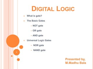
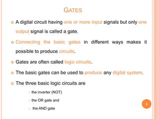
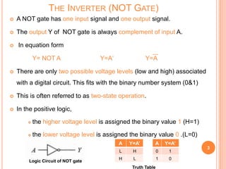
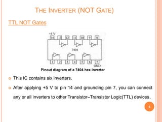
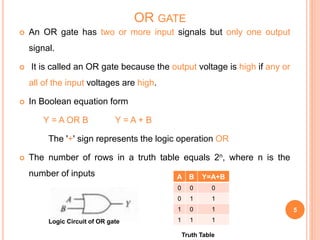
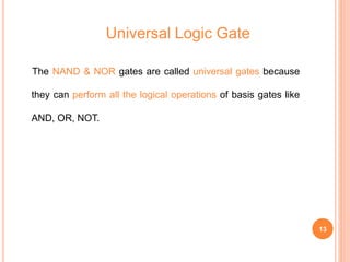
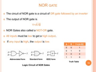
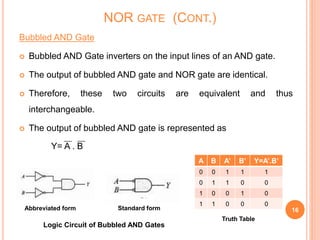
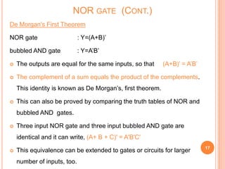
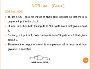
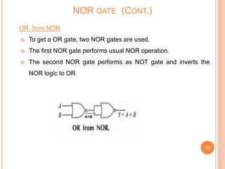
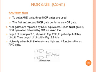
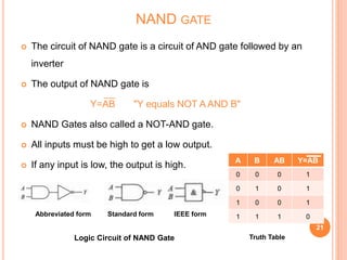
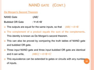
DIGITAL LOGIC
 What is gate?
 The Basic Gates
 NOT gate
 OR gate
 AND gate
 Universal Logic Gates
 NOR gate
 NAND gate
1
Presented by,
M.Madhu Bala
GATES
 A digital circuit having one or more input signals but only one
output signal is called a gate.
 Connecting the basic gates in different ways makes it
possible to produce circuits.
 Gates are often called logic circuits.
 The basic gates can be used to produce any digital system.
 The three basic logic circuits are
 the inverter (NOT)
 the OR gate and
 the AND gate
2
THE INVERTER (NOT GATE)
 A NOT gate has one input signal and one output signal.
 The output Y of NOT gate is always complement of input A.
 In equation form
Y= NOT A Y=A‘ Y=A
 There are only two possible voltage levels (low and high) associated
with a digital circuit. This fits with the binary number system (0&1)
 This is often referred to as two-state operation.
 In the positive logic,
 the higher voltage level is assigned the binary value 1 (H=1)
 the lower voltage level is assigned the binary value 0 .(L=0)
3
A Y=A’
L H
H L
A Y=A’
0 1
1 0
Logic Circuit of NOT gate
Truth Table
THE INVERTER (NOT GATE)
TTL NOT Gates
Pinout diagram of a 7404 hex inverter
 This IC contains six inverters.
 After applying +5 V to pin 14 and grounding pin 7, you can connect
any or all inverters to other Transistor–Transistor Logic(TTL) devices.
4
OR GATE
 An OR gate has two or more input signals but only one output
signal.
 It is called an OR gate because the output voltage is high if any or
all of the input voltages are high.
 In Boolean equation form
Y = A OR B Y = A + B
The '+' sign represents the logic operation OR
 The number of rows in a truth table equals 2n, where n is the
number of inputs
5
Logic Circuit of OR gate
A B Y=A+B
0 0 0
0 1 1
1 0 1
1 1 1
Truth Table
Three- input OR gate
 The inputs are A, B, and C.
 When all inputs are low, the output is low.
 If any input is high, the output will be high.
 Boolean Equation Form:
Y = A+B+C
6
OR GATE (CONT..)
A B C Y=A+B+C
0 0 0 0
0 0 1 1
0 1 0 1
0 1 1 1
1 0 0 1
1 0 1 1
1 1 0 1
1 1 1 1Logic Circuit of 3-input OR gate
Truth Table
TTL OR Gates
This digital IC contains four 2-input OR gates inside a 14-
pin DIP.
After connecting a supply voltage of +5 V to pin 14 and a
ground to pin 7, you can connect one or more of the OR
gates to other TTL devices.
7
OR GATE (CONT.)
Timing diagram for 2-input OR gate
 The input voltages drive pins 1 and 2 of a 7432.
 The output (pin 3) is low only when both inputs are low.
 The output is high the rest of the time.
8
OR GATE (CONT..)
 The AND gate has a high output only when all inputs are high.
otherwise the output will be low.
 AND gate also known as all-or-nothing gate.
 In Boolean equation form
Y =A AND B Y=A.B Y=AB
The '.' sign represents the logic AND operation.
9
AND GATE
A B Y=AB
0 0 0
0 1 0
1 0 0
1 1 1Logic Circuit of AND gate
Truth Table
Three- input AND gate
 The inputs are A, B, and C.
 When all inputs are high, the output is high.
 If even one input is low, the output is in the low state.
 In Boolean equation form:
Y=A.B.C Y=ABC
10
AND GATE (CONT..)
A B C Y=ABC
0 0 0 0
0 0 1 0
0 1 0 0
0 1 1 0
1 0 0 0
1 0 1 0
1 1 0 0
1 1 1 1
Logic Circuit of AND gate
Truth Table
TTL AND Gates
 This digital IC contains four 2-input AND gates.
 After connecting a supply voltage of +5V to pin 14 and a ground to
pin 7, you can connect one or more of the AND gates to other TTL
devices.
 TTL AND gates are also available in triple 3-input and dual 4-input
packages.
11
AND GATE (CONT..)
Timing diagram for a 2-input AND gate
The input voltages drive pins 1 and 2 of a 7408.
the output (pin 3) is high only when both inputs are high.
The output is low the rest of the time.
12
AND GATE (CONT..)
The NAND & NOR gates are called universal gates because
they can perform all the logical operations of basis gates like
AND, OR, NOT.
13
Universal Logic Gate
 The circuit of NOR gate is a circuit of OR gate followed by an inverter
 The output of NOR gate is
Y=A+B
 NOR Gates also called a NOT-OR gate.
 All inputs must be low to get a high output.
 If any input is high, the output is low.
14
NOR GATE
Logic Circuit of NOR Gates
Abbreviated form Standard form IEEE form
Truth Table
A B Y=(A+B)’
0 0 1
0 1 0
1 0 0
1 1 0
Pin- out Diagram of NOR gate
15
NOR GATE (CONT.)
Bubbled AND Gate
 Bubbled AND Gate inverters on the input lines of an AND gate.
 The output of bubbled AND gate and NOR gate are identical.
 Therefore, these two circuits are equivalent and thus
interchangeable.
 The output of bubbled AND gate is represented as
Y= A . B
16
NOR GATE (CONT.)
Abbreviated form Standard form
Truth Table
A B A’ B’ Y=A’.B’
0 0 1 1 1
0 1 1 0 0
1 0 0 1 0
1 1 0 0 0
Logic Circuit of Bubbled AND Gates
De Morgan's First Theorem
NOR gate : Y=(A+B)’
bubbled AND gate : Y=A’B’
 The outputs are equal for the same inputs, so that (A+B)’ = A’B’
 The complement of a sum equals the product of the complements.
This identity is known as De Morgan’s, first theorem.
 This can also be proved by comparing the truth tables of NOR and
bubbled AND gates.
 Three input NOR gate and three input bubbled AND gate are
identical and it can write, (A+ B + C)' = A'B'C'
 This equivalence can be extended to gates or circuits for larger
number of inputs, too.
17
NOR GATE (CONT.)
NOT from NOR
 To get a NOT gate, tie inputs of NOR gate together so that there is
only one input to the circuit.
 If input is 0, then both the inputs to NOR gate are 0 that gives output
1.
 Similarly, if input is 1, both the inputs to NOR gate are 1 that gives
output 0.
 Therefore the output of circuit is complement of its input and thus
gives NOT operation.
18
NOR GATE (CONT.)
OR from NOR
 To get a OR gate, two NOR gates are used.
 The first NOR gate performs usual NOR operation.
 The second NOR gate performs as NOT gate and inverts the
NOR logic to OR
19
NOR GATE (CONT.)
A+B
AND from NOR
 To get a AND gate, three NOR gates are used.
 The first and second NOR gate performs as NOT gate.
 NOT gates are replaced by NOR equivalent. Since NOR gate is
NOT operation followed by OR we invert the
 output of example 2.3, shown in Fig. 2.9b to get output of this
circuit. Thus output of circuit in Fig. 2.2 lc is
 high only when both the inputs are high and it functions like an
AND gate.
20
NOR GATE (CONT.)
 The circuit of NAND gate is a circuit of AND gate followed by an
inverter
 The output of NAND gate is
Y=AB "Y equals NOT A AND B"
 NAND Gates also called a NOT-AND gate.
 All inputs must be high to get a low output.
 If any input is low, the output is high.
21
NAND GATE
Logic Circuit of NAND Gate
Abbreviated form Standard form IEEE form
Truth Table
A B AB Y=AB
0 0 0 1
0 1 0 1
1 0 0 1
1 1 1 0
Pin- out Diagram of NAND gate
22
NAND GATE (CONT.)
Bubbled OR Gate
 Bubbled OR Gate inverters on the input lines of an OR gate.
 The output of bubbled OR gate and NAND gate are identical.
 Therefore, these two circuits are equivalent and thus
interchangeable.
 The output of bubbled OR gate is represented as
Y=A+B
23
NAND GATE (CONT.)
A B A B Y=A+B
0 0 1 1 1
0 1 1 0 1
1 0 0 1 1
1 1 0 0 0
Abbreviated form Standard form
Truth TableLogic Circuit of Bubbled OR Gate
De Morgan's Second Theorem
NAND Gate :(AB)’
Bubbled OR Gate : Y=A’+B’
 The outputs are equal for the same inputs, so that (AB)’ = A’+B’
 The complement of a product equals the sum of the complements.
This identity is known as De Morgan’s second theorem.
 This can also be proved by comparing the truth tables of NAND gate
and bubbled OR gate.
 Three input NAND gate and three input bubbled OR gate are identical
and it can write, (ABC)' = A’+B‘+C’
 This equivalence can be extended to gates or circuits with any number
of inputs.
24
NAND GATE (CONT.)
THANK YOU
25

Digital logic

  • 1.
    DIGITAL LOGIC  Whatis gate?  The Basic Gates  NOT gate  OR gate  AND gate  Universal Logic Gates  NOR gate  NAND gate 1 Presented by, M.Madhu Bala
  • 2.
    GATES  A digitalcircuit having one or more input signals but only one output signal is called a gate.  Connecting the basic gates in different ways makes it possible to produce circuits.  Gates are often called logic circuits.  The basic gates can be used to produce any digital system.  The three basic logic circuits are  the inverter (NOT)  the OR gate and  the AND gate 2
  • 3.
    THE INVERTER (NOTGATE)  A NOT gate has one input signal and one output signal.  The output Y of NOT gate is always complement of input A.  In equation form Y= NOT A Y=A‘ Y=A  There are only two possible voltage levels (low and high) associated with a digital circuit. This fits with the binary number system (0&1)  This is often referred to as two-state operation.  In the positive logic,  the higher voltage level is assigned the binary value 1 (H=1)  the lower voltage level is assigned the binary value 0 .(L=0) 3 A Y=A’ L H H L A Y=A’ 0 1 1 0 Logic Circuit of NOT gate Truth Table
  • 4.
    THE INVERTER (NOTGATE) TTL NOT Gates Pinout diagram of a 7404 hex inverter  This IC contains six inverters.  After applying +5 V to pin 14 and grounding pin 7, you can connect any or all inverters to other Transistor–Transistor Logic(TTL) devices. 4
  • 5.
    OR GATE  AnOR gate has two or more input signals but only one output signal.  It is called an OR gate because the output voltage is high if any or all of the input voltages are high.  In Boolean equation form Y = A OR B Y = A + B The '+' sign represents the logic operation OR  The number of rows in a truth table equals 2n, where n is the number of inputs 5 Logic Circuit of OR gate A B Y=A+B 0 0 0 0 1 1 1 0 1 1 1 1 Truth Table
  • 6.
    Three- input ORgate  The inputs are A, B, and C.  When all inputs are low, the output is low.  If any input is high, the output will be high.  Boolean Equation Form: Y = A+B+C 6 OR GATE (CONT..) A B C Y=A+B+C 0 0 0 0 0 0 1 1 0 1 0 1 0 1 1 1 1 0 0 1 1 0 1 1 1 1 0 1 1 1 1 1Logic Circuit of 3-input OR gate Truth Table
  • 7.
    TTL OR Gates Thisdigital IC contains four 2-input OR gates inside a 14- pin DIP. After connecting a supply voltage of +5 V to pin 14 and a ground to pin 7, you can connect one or more of the OR gates to other TTL devices. 7 OR GATE (CONT.)
  • 8.
    Timing diagram for2-input OR gate  The input voltages drive pins 1 and 2 of a 7432.  The output (pin 3) is low only when both inputs are low.  The output is high the rest of the time. 8 OR GATE (CONT..)
  • 9.
     The ANDgate has a high output only when all inputs are high. otherwise the output will be low.  AND gate also known as all-or-nothing gate.  In Boolean equation form Y =A AND B Y=A.B Y=AB The '.' sign represents the logic AND operation. 9 AND GATE A B Y=AB 0 0 0 0 1 0 1 0 0 1 1 1Logic Circuit of AND gate Truth Table
  • 10.
    Three- input ANDgate  The inputs are A, B, and C.  When all inputs are high, the output is high.  If even one input is low, the output is in the low state.  In Boolean equation form: Y=A.B.C Y=ABC 10 AND GATE (CONT..) A B C Y=ABC 0 0 0 0 0 0 1 0 0 1 0 0 0 1 1 0 1 0 0 0 1 0 1 0 1 1 0 0 1 1 1 1 Logic Circuit of AND gate Truth Table
  • 11.
    TTL AND Gates This digital IC contains four 2-input AND gates.  After connecting a supply voltage of +5V to pin 14 and a ground to pin 7, you can connect one or more of the AND gates to other TTL devices.  TTL AND gates are also available in triple 3-input and dual 4-input packages. 11 AND GATE (CONT..)
  • 12.
    Timing diagram fora 2-input AND gate The input voltages drive pins 1 and 2 of a 7408. the output (pin 3) is high only when both inputs are high. The output is low the rest of the time. 12 AND GATE (CONT..)
  • 13.
    The NAND &NOR gates are called universal gates because they can perform all the logical operations of basis gates like AND, OR, NOT. 13 Universal Logic Gate
  • 14.
     The circuitof NOR gate is a circuit of OR gate followed by an inverter  The output of NOR gate is Y=A+B  NOR Gates also called a NOT-OR gate.  All inputs must be low to get a high output.  If any input is high, the output is low. 14 NOR GATE Logic Circuit of NOR Gates Abbreviated form Standard form IEEE form Truth Table A B Y=(A+B)’ 0 0 1 0 1 0 1 0 0 1 1 0
  • 15.
    Pin- out Diagramof NOR gate 15 NOR GATE (CONT.)
  • 16.
    Bubbled AND Gate Bubbled AND Gate inverters on the input lines of an AND gate.  The output of bubbled AND gate and NOR gate are identical.  Therefore, these two circuits are equivalent and thus interchangeable.  The output of bubbled AND gate is represented as Y= A . B 16 NOR GATE (CONT.) Abbreviated form Standard form Truth Table A B A’ B’ Y=A’.B’ 0 0 1 1 1 0 1 1 0 0 1 0 0 1 0 1 1 0 0 0 Logic Circuit of Bubbled AND Gates
  • 17.
    De Morgan's FirstTheorem NOR gate : Y=(A+B)’ bubbled AND gate : Y=A’B’  The outputs are equal for the same inputs, so that (A+B)’ = A’B’  The complement of a sum equals the product of the complements. This identity is known as De Morgan’s, first theorem.  This can also be proved by comparing the truth tables of NOR and bubbled AND gates.  Three input NOR gate and three input bubbled AND gate are identical and it can write, (A+ B + C)' = A'B'C'  This equivalence can be extended to gates or circuits for larger number of inputs, too. 17 NOR GATE (CONT.)
  • 18.
    NOT from NOR To get a NOT gate, tie inputs of NOR gate together so that there is only one input to the circuit.  If input is 0, then both the inputs to NOR gate are 0 that gives output 1.  Similarly, if input is 1, both the inputs to NOR gate are 1 that gives output 0.  Therefore the output of circuit is complement of its input and thus gives NOT operation. 18 NOR GATE (CONT.)
  • 19.
    OR from NOR To get a OR gate, two NOR gates are used.  The first NOR gate performs usual NOR operation.  The second NOR gate performs as NOT gate and inverts the NOR logic to OR 19 NOR GATE (CONT.) A+B
  • 20.
    AND from NOR To get a AND gate, three NOR gates are used.  The first and second NOR gate performs as NOT gate.  NOT gates are replaced by NOR equivalent. Since NOR gate is NOT operation followed by OR we invert the  output of example 2.3, shown in Fig. 2.9b to get output of this circuit. Thus output of circuit in Fig. 2.2 lc is  high only when both the inputs are high and it functions like an AND gate. 20 NOR GATE (CONT.)
  • 21.
     The circuitof NAND gate is a circuit of AND gate followed by an inverter  The output of NAND gate is Y=AB "Y equals NOT A AND B"  NAND Gates also called a NOT-AND gate.  All inputs must be high to get a low output.  If any input is low, the output is high. 21 NAND GATE Logic Circuit of NAND Gate Abbreviated form Standard form IEEE form Truth Table A B AB Y=AB 0 0 0 1 0 1 0 1 1 0 0 1 1 1 1 0
  • 22.
    Pin- out Diagramof NAND gate 22 NAND GATE (CONT.)
  • 23.
    Bubbled OR Gate Bubbled OR Gate inverters on the input lines of an OR gate.  The output of bubbled OR gate and NAND gate are identical.  Therefore, these two circuits are equivalent and thus interchangeable.  The output of bubbled OR gate is represented as Y=A+B 23 NAND GATE (CONT.) A B A B Y=A+B 0 0 1 1 1 0 1 1 0 1 1 0 0 1 1 1 1 0 0 0 Abbreviated form Standard form Truth TableLogic Circuit of Bubbled OR Gate
  • 24.
    De Morgan's SecondTheorem NAND Gate :(AB)’ Bubbled OR Gate : Y=A’+B’  The outputs are equal for the same inputs, so that (AB)’ = A’+B’  The complement of a product equals the sum of the complements. This identity is known as De Morgan’s second theorem.  This can also be proved by comparing the truth tables of NAND gate and bubbled OR gate.  Three input NAND gate and three input bubbled OR gate are identical and it can write, (ABC)' = A’+B‘+C’  This equivalence can be extended to gates or circuits with any number of inputs. 24 NAND GATE (CONT.)
  • 25.