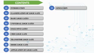
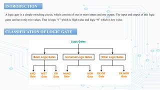
INTRODUCTION
A logic gateis a simple switching circuit, which consists of one or more inputs and one output. The input and output of this logic
gates can have only two values. That is logic “1” which is High value and logic “0” which is low value.
CLASSIFICATION OF LOGIC GATE
4.
BASIC LOGIC GATES
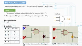
ANDGATE:
• The output of AND gate is high (‘1’) if all of its inputs are high (‘1’).
• The output of AND gate is low (‘0’) if any one of its inputs is low (‘0’).
Logical Expression:
Y = A.B
Truth Table:
A B Y = A. B
0 0 0
0 1 0
1 0 0
1 1 1
Operation:
Symbol:
Fig-1.1: And Gate, when either of one input is Fig-1.2: And Gate, when two one inputs are high
Basic Logic Gates are three types: (1) AND Gate, (2) OR Gate, (3) NOT Gate
5.
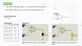
OR GATE:
• Theoutput of OR gate is high (‘1’) if any one of its input is high (‘1’).
• The output of OR gate is low (‘0’) if all of its inputs are low (‘0’).
Logical Expression:
Y = A +B
Truth Table:
A B Y = A + B
0 0 0
0 1 1
1 0 1
1 1 1
Symbol:
Operation:
Fig-2.1: OR Gate, when two inputs are low Fig-2.2: OR Gate, when either of one input is
high
6.
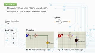
NOT GATE:
• Theoutput of NOT gate is high (‘1’) if its input is low (‘0’).
• The output of NOT gate is low (‘0’) if its input is high (‘1’).
Logical Expression:
Y=A
Truth Table:
A Y = A’
0 1
1 0
Symbol:
Operation:
Fig-3.1: NOT Gate, when input is low. Fig-3.2: NOT Gate, when input is high.
7.
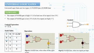
UNIVERSAL LOGIC GATES
UniversalLogic Gates are two types: (1) NAND Gate, (2) NOR Gate
Truth Table:
• The output of NAND gate is high (‘1’) if at least one of its input is low (‘0’)
• The output of NAND gate is low (‘0’) if all of its inputs are high (‘1’).
Logical Expression:
Y = A. B
NAND GATE:
A B Y = (A. B)’
0 0 1
0 1 1
1 0 1
1 1 0
Operation:
Fig-4.1: NAND Gate, when either of one input
is low.
Fig-4.2: NAND Gate, when two inputs are high.
Symbol:
8.
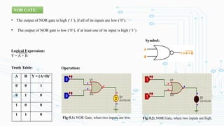
NOR GATE:
• Theoutput of NOR gate is high (‘1’), if all of its inputs are low (‘0’).
• The output of NOR gate is low (‘0’), if at least one of its input is high (‘1’)
Logical Expression:
Y = A + B
Truth Table:
A B Y = (A+B)’
0 0 1
0 1 0
1 0 0
1 1 0
Operation:
Symbol:
Fig-5.1: NOR Gate, when two inputs are low. Fig-5.2: NOR Gate, when two inputs are high.
9.
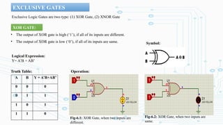
EXCLUSIVE GATES
Exclusive LogicGates are two type: (1) XOR Gate, (2) XNOR Gate
XOR GATE:
• The output of XOR gate is high (‘1’), if all of its inputs are different.
• The output of XOR gate is low (‘0’), if all of its inputs are same.
Logical Expression:
Y= A’B + AB’
Truth Table:
A B Y = A’B+AB’
0 0 0
0 1 1
1 0 1
1 1 0
Symbol:
Operation:
Fig-6.1: XOR Gate, when two inputs are
different.
Fig-6.2: XOR Gate, when two inputs are
same.
10.
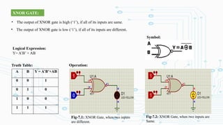
XNOR GATE:
• Theoutput of XNOR gate is high (‘1’), if all of its inputs are same.
• The output of XNOR gate is low (‘1’), if all of its inputs are different.
Logical Expression:
Y= A’B’ + AB
Truth Table:
A B Y = A’B’+AB
0 0 1
0 1 0
1 0 0
1 1 1
Symbol:
Operation:
Fig-7.1: XNOR Gate, when two inputs
are different.
Fig-7.2: XNOR Gate, when two inputs are
Same.
11.
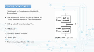
CMOS LOGIC GATE
•CMOS stands for Complementary Metal Oxide
Semiconductor.
• PMOS transistors are used as a pull-up network and
NMOS transistors are used as a pull-down network.
• Pull-up network to supply voltage Vcc.
• One is conducting, while the other isn’t.
• NMOS only
• Pull-down network to ground.
• PMOS only
Fig-8.1: CMOS Logic Gate
12.
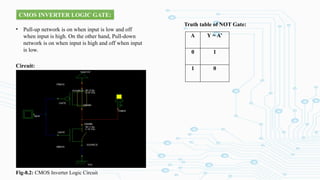
CMOS INVERTER LOGICGATE:
• Pull-up network is on when input is low and off
when input is high. On the other hand, Pull-down
network is on when input is high and off when input
is low.
Fig-8.2: CMOS Inverter Logic Circuit
A Y = A’
0 1
1 0
Truth table of NOT Gate:
Circuit:
13.
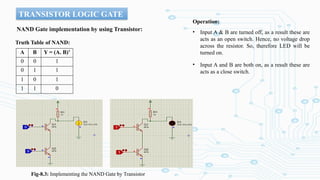
TRANSISTOR LOGIC GATE
NANDGate implementation by using Transistor:
A B Y = (A. B)’
0 0 1
0 1 1
1 0 1
1 1 0
Truth Table of NAND:
Fig-8.3: Implementing the NAND Gate by Transistor
Operation:
• Input A & B are turned off, as a result these are
acts as an open switch. Hence, no voltage drop
across the resistor. So, therefore LED will be
turned on.
• Input A and B are both on, as a result these are
acts as a close switch.
14.
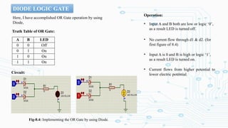
DIODE LOGIC GATE
Here,I have accomplished OR Gate operation by using
Diode,
Truth Table of OR Gate:
A B LED
0 0 Off
0 1 On
1 0 On
1 1 On
Circuit:
Fig-8.4: Implementing the OR Gate by using Diode.
Operation:
• Input A and B both are low or logic ‘0’,
as a result LED is turned off.
• No current flow through d1 & d2. (for
first figure of 8.4)
• Input A is 0 and B is high or logic ‘1’,
as a result LED is turned on.
• Current flows from higher potential to
lower electric potential.
15.
APPLICATION OF LOGICGATES
• Used in microcontrollers, microprocessors, electronic and electrical project circuits, and embedded system applications.
• Also used in many circuits like a push button lock, light activated burglar alarm, safety thermostat etc.
• In digital processing of communications.
• In calculators and computers.
• They are also used in push button switches, e.g. door bell, TTL (Transistor Transistor Logic) and CMOS circuitry.
16.
CONCLUSION
Logic gates orcircuits can be implemented by using electronics components (diodes, transistors and resistors etc.) and
verified by the helps of Boolean expressions, truth tables, and logic diagrams. There are several types of logic gates,
including AND, OR, NOT, NAND, NOR, XOR and XNOR gates, each with a unique truth table and behavior. Digital
communication can’t happen without logic operations.