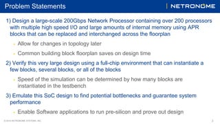
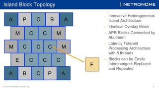
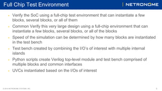
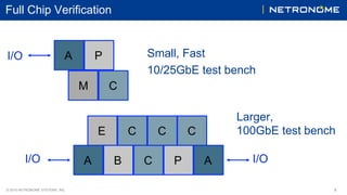
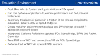
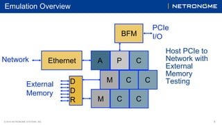
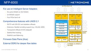
© 2016 NETRONOME SYSTEMS, INC.
Ron Swartzentruber
CDN Live April 5, 2016
Design, Verification and
Emulation of an Island-Based
Network Flow Processor
1
© 2016 NETRONOME SYSTEMS, INC. 2
Problem Statements
1) Design a large-scale 200Gbps Network Processor containing over 200 processors
with multiple high speed I/O and large amounts of internal memory using APR
blocks that can be replaced and interchanged across the floorplan
▶ Allow for changes in topology later
▶ Common building block floorplan saves on design time
2) Verify this very large design using a full-chip environment that can instantiate a
few blocks, several blocks, or all of the blocks
▶ Speed of the simulation can be determined by how many blocks are
instantiated in the testbench
3) Emulate this SoC design to find potential bottlenecks and guarantee system
performance
▶ Enable Software applications to run pre-silicon and prove out design
© 2016 NETRONOME SYSTEMS, INC. 3
Building an NFP Island
APR Blocks with a Common
Footprint
External Signal Interconnect
with Fixed Pin Locations
▶ Fabric Ports
▶ Register Interface
▶ Interrupts and Events
▶ JTAG, Clocks, DFT
Re-use I/O Timing constraints
50/50 budget
Common Test Logic, complete
for DFM
• Identical Overlay
Mesh for Internal
Signals and Busses
for all Islands
NFP Island
Interconnect
Mesh
© 2016 NETRONOME SYSTEMS, INC. 4
Island Block Topology
▶ Innovative Heterogeneous
Island Architecture
▶ Identical Overlay Mesh
▶ APR Blocks Connected by
Abutment
▶ Latency Tolerant
Processing Architecture
with 8 threads
▶ Blocks can be Easily
Interchanged; Replaced
and Repeated
M C C M
C C C
P C B A
M
A
E C C C
B C P AA
F
M
© 2016 NETRONOME SYSTEMS, INC. 5
Full Chip Test Environment
▶ Verify the SoC using a full-chip test environment that can instantiate a few
blocks, several blocks, or all of them
▶ Common Verify this very large design using a full-chip environment that can
instantiate a few blocks, several blocks, or all of the blocks
▶ Speed of the simulation can be determined by how many blocks are instantiated
in the test bench
▶ Test bench created by combining the I/O’s of interest with multiple internal
islands
▶ Python scripts create Verilog top-level module and test bench comprised of
multiple blocks and common interfaces
▶ UVCs instantiated based on the I/Os of interest
© 2016 NETRONOME SYSTEMS, INC. 6
Full Chip Verification
Small, Fast
10/25GbE test bench
M C
PA
E C C C
B C P AA
I/O
I/O I/O
Larger,
100GbE test bench
© 2016 NETRONOME SYSTEMS, INC. 7
Emulation Environment
▶ Goal: Run full chip System Verilog simulations at 20x speed
▶ Run real Software applications to validate performance and find potential
bottlenecks
▶ Test many thousands of packets in a fraction of the time as compared to
simulation. Goal: 9,000x w/ speed-bridge(s)
▶ Create make/run environment that allows any SW engineer to test NFP
application code pre-silicon
▶ Incorporate Cadence Palladium supported I/Os, Speedbridge, BFMs and Packet
Generator
▶ Treat DUT as a “NIC” and connect to a VM via PCIe Speedbridge
▶ Software load to “NIC” via external PCIe interface
© 2016 NETRONOME SYSTEMS, INC. 8
Emulation Overview
Host PCIe to
Network with
External
Memory
Testing
EthernetNetwork
M C C
C C
P CA
M
D
D
R
External
Memory
BFM
PCIe
I/O
© 2016 NETRONOME SYSTEMS, INC. 9
NFP-6000
For use on Intelligent Server Adapters
▶ Six ports 40GbE (or 24x10GbE)
▶ 2x100GbE support
▶ Four PCIe Gen3 x8
Comprehensive features with LNOD 2.1
▶ RX/TX with SR-IOV and stateless offloads
▶ Extensive, flexible tunneling support (e.g. VXLAN, GRE)
▶ Transparent offload of OVS datapath
▶ Stateful flow tracking
▶ Stateful Load Balancing
Firmware Data Plane (blue)
External DDR3 for deeper flow tables
PCIe Gen3
x 8
RX & TX Processing Adaptive Memory
Controller
(DDR3-2133)
Internal
Memory Unit
External
Memory
Unit
Load Balancing
Flow Tracker
OVS 2.3.9
VXLAN/GRE
RX/TX DMA
Function Accelerators
Hash Queue
AtomicTM
Bulk Crypto …
Network Interface
MAC SerDes
4x PCIe Gen3 x8
2x100GbE, 6x 40GbE or
24x10GE
6x32bit
DDR3
PCIe Gen3
x 8
PCIe Gen3
x 8
PCIe Gen3
x 8
© 2016 NETRONOME SYSTEMS, INC. 10
Reference Patents
▶ US Patent Application No. 13/399,433: Staggered Island Structure in an Island-
based Network Flow Processor
▶ US Patent Application No. 13/399,888: Island-based Network Flow Processor
Integrated Circuit
▶ US Patent Application No. 13/399,958: Processing Resource Management in an
Island-based Network Flow Processor
© 2016 NETRONOME SYSTEMS, INC.
Thank You

Design, Verification and Emulation of an Island-Based Network Flow Processor

  • 1.
    © 2016 NETRONOMESYSTEMS, INC. Ron Swartzentruber CDN Live April 5, 2016 Design, Verification and Emulation of an Island-Based Network Flow Processor 1
  • 2.
    © 2016 NETRONOMESYSTEMS, INC. 2 Problem Statements 1) Design a large-scale 200Gbps Network Processor containing over 200 processors with multiple high speed I/O and large amounts of internal memory using APR blocks that can be replaced and interchanged across the floorplan ▶ Allow for changes in topology later ▶ Common building block floorplan saves on design time 2) Verify this very large design using a full-chip environment that can instantiate a few blocks, several blocks, or all of the blocks ▶ Speed of the simulation can be determined by how many blocks are instantiated in the testbench 3) Emulate this SoC design to find potential bottlenecks and guarantee system performance ▶ Enable Software applications to run pre-silicon and prove out design
  • 3.
    © 2016 NETRONOMESYSTEMS, INC. 3 Building an NFP Island APR Blocks with a Common Footprint External Signal Interconnect with Fixed Pin Locations ▶ Fabric Ports ▶ Register Interface ▶ Interrupts and Events ▶ JTAG, Clocks, DFT Re-use I/O Timing constraints 50/50 budget Common Test Logic, complete for DFM • Identical Overlay Mesh for Internal Signals and Busses for all Islands NFP Island Interconnect Mesh
  • 4.
    © 2016 NETRONOMESYSTEMS, INC. 4 Island Block Topology ▶ Innovative Heterogeneous Island Architecture ▶ Identical Overlay Mesh ▶ APR Blocks Connected by Abutment ▶ Latency Tolerant Processing Architecture with 8 threads ▶ Blocks can be Easily Interchanged; Replaced and Repeated M C C M C C C P C B A M A E C C C B C P AA F M
  • 5.
    © 2016 NETRONOMESYSTEMS, INC. 5 Full Chip Test Environment ▶ Verify the SoC using a full-chip test environment that can instantiate a few blocks, several blocks, or all of them ▶ Common Verify this very large design using a full-chip environment that can instantiate a few blocks, several blocks, or all of the blocks ▶ Speed of the simulation can be determined by how many blocks are instantiated in the test bench ▶ Test bench created by combining the I/O’s of interest with multiple internal islands ▶ Python scripts create Verilog top-level module and test bench comprised of multiple blocks and common interfaces ▶ UVCs instantiated based on the I/Os of interest
  • 6.
    © 2016 NETRONOMESYSTEMS, INC. 6 Full Chip Verification Small, Fast 10/25GbE test bench M C PA E C C C B C P AA I/O I/O I/O Larger, 100GbE test bench
  • 7.
    © 2016 NETRONOMESYSTEMS, INC. 7 Emulation Environment ▶ Goal: Run full chip System Verilog simulations at 20x speed ▶ Run real Software applications to validate performance and find potential bottlenecks ▶ Test many thousands of packets in a fraction of the time as compared to simulation. Goal: 9,000x w/ speed-bridge(s) ▶ Create make/run environment that allows any SW engineer to test NFP application code pre-silicon ▶ Incorporate Cadence Palladium supported I/Os, Speedbridge, BFMs and Packet Generator ▶ Treat DUT as a “NIC” and connect to a VM via PCIe Speedbridge ▶ Software load to “NIC” via external PCIe interface
  • 8.
    © 2016 NETRONOMESYSTEMS, INC. 8 Emulation Overview Host PCIe to Network with External Memory Testing EthernetNetwork M C C C C P CA M D D R External Memory BFM PCIe I/O
  • 9.
    © 2016 NETRONOMESYSTEMS, INC. 9 NFP-6000 For use on Intelligent Server Adapters ▶ Six ports 40GbE (or 24x10GbE) ▶ 2x100GbE support ▶ Four PCIe Gen3 x8 Comprehensive features with LNOD 2.1 ▶ RX/TX with SR-IOV and stateless offloads ▶ Extensive, flexible tunneling support (e.g. VXLAN, GRE) ▶ Transparent offload of OVS datapath ▶ Stateful flow tracking ▶ Stateful Load Balancing Firmware Data Plane (blue) External DDR3 for deeper flow tables PCIe Gen3 x 8 RX & TX Processing Adaptive Memory Controller (DDR3-2133) Internal Memory Unit External Memory Unit Load Balancing Flow Tracker OVS 2.3.9 VXLAN/GRE RX/TX DMA Function Accelerators Hash Queue AtomicTM Bulk Crypto … Network Interface MAC SerDes 4x PCIe Gen3 x8 2x100GbE, 6x 40GbE or 24x10GE 6x32bit DDR3 PCIe Gen3 x 8 PCIe Gen3 x 8 PCIe Gen3 x 8
  • 10.
    © 2016 NETRONOMESYSTEMS, INC. 10 Reference Patents ▶ US Patent Application No. 13/399,433: Staggered Island Structure in an Island- based Network Flow Processor ▶ US Patent Application No. 13/399,888: Island-based Network Flow Processor Integrated Circuit ▶ US Patent Application No. 13/399,958: Processing Resource Management in an Island-based Network Flow Processor
  • 11.
    © 2016 NETRONOMESYSTEMS, INC. Thank You