Download to read offline


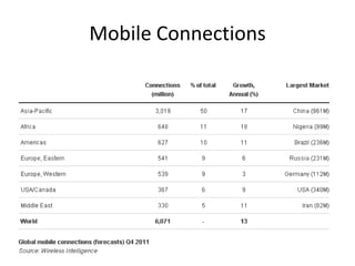

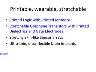


This document discusses several emerging technologies including: 1) Google voice translation tools that allow instant translation between 14 languages with the press of a button. 2) The number of mobile connections reaching 6 billion this year, highlighting the importance of translation technologies. 3) Research into quantum computing using nitrogen vacancy diamond and photonic approaches, as well as supercomputers scaling to exaflop speeds. 4) Developments in printed, wearable, and stretchable electronics including circuits, memory, sensors and brain implants.


