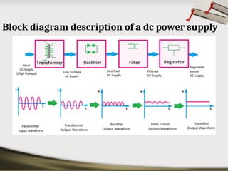
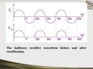
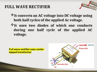
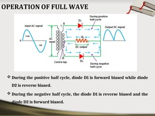
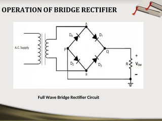
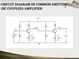
Basic Electrical and Electronics Engineering
Part – B
Unit 2 – BASIC ELECTRONIC CIRCUITS &
INSTRUMENTATION
By
Dr.S.A.Sivakumar [Dean-Academics, ASKW]
Mr.B.Naga Rajesh(Ph.D) [AP-ECE, ASKW]
Block diagram description of a dc power supply
Transformer
•The transformer is a device that transfers the electrical
energy from one circuit to another circuit by changing the
voltage level.
•Here, in the above, a step-down transformer is used that is
used to step down the voltage.
• Generally, it takes the 220V supply as input and provides 12V
or 24V or 6V as the output according to the circuit output
requirement.
Rectifier
• The main function of the rectifier circuit is to convert
the AC supply into a DC supply.
• It takes the Alternating current or AC power supply as
input and gives the direct current or DC power supply
as output.
• The rectifier is the second block of the regulated power
supply.
Filter
• The output of the rectifier circuit cannot provide the pure DC
supply.
• There are some ripple or AC components available in the DC power
supply.
• To remove those ripples or make the DC supply pure, a filter circuit
is used.
• The output of the rectifier is connected to the input of the filter
circuit.
• Generally, a pure capacitor filter, LC filter, or pi filter is used.
Regulator
• It is the last and most important block of the regulated
power supply.
• The regulator actually does the regulation.
• A Zener diode can regulate voltage by just connecting it in
reverse bias.
• IC 7805 is the most common usable regulator IC.
• It always provides a constant 5V DC voltage as its output.
WHAT IS A RECTIFIER……?
 A rectifier is an electronic device that converts an
alternating current into a direct current by using
one or more P-N junction diodes.
 A diode behaves as a one-way valve that allows
current to flow in a single direction. This process is
known as rectification.
• Rectifiers are of two types:
Half Wave Rectifier
Full Wave Rectifier
Bridge Rectifier
• A half-wave rectifier is the simplest form of the
rectifier and requires only one diode for the
construction of a halfwave rectifier circuit.
• In a half wave rectifier, rectifying element conducts
only during positive half cycle of input AC supply.
• The negative half cycle of AC supply is eliminated
from the output.
• A halfwave rectifier circuit consists of three main
components as follows:
 A diode
 A transformer
 A resistive load
1. A high AC voltage is applied to the primary side of the step-down
transformer. The obtained secondary low voltage is applied to the
diode.
2. The diode is forward biased during the positive half cycle of the AC
voltage and reverse biased during the negative half cycle.
For the positive half
cycle of the AC source
voltage, the circuit
effectively becomes as
shown in the figure
For the negative half
cycle of the AC source
voltage, the equivalent
circuit becomes as
shown in the figure
The halfwave rectifier waveform before and after
rectification.
It converts an AC voltage into DC voltage using
both half cycles of the applied Ac voltage.
It uses two diodes of which one conducts
during one half cycle of the applied AC
voltage.
 During the positive half cycle, diode D1 is forward biased while diode
D2 is reverse biased.
 During the negative half cycle, the diode D1 is reverse biased and the
diode D2 is forward biased.
It has four diodes connected to form a bridge.
AC input voltage is applied to diagonally opposite
ends of the bridge.
The load resistance is connected in between the
other two ends of the bridge.
Full Wave Bridge Rectifier Circuit
When an ac signal is applied across the bridge rectifier, terminal A
becomes positive during the positive half cycle while terminal B becomes
negative. this results in diodes D1 and D3 becoming forward biased while
D2 and D4 becoming reverse biased.
During the negative half-cycle, terminal B becomes positive while
terminal A becomes negative. This causes diodes D2 and D4 to become
forward biased and diode D1 and D3 to be reverse biased.
OUTPUT WAVEFORM
The DC output produced by the bridge rectifier is not a pure DC but a
pulsating DC. This pulsating DC contains both AC and DC components.
FULL WAVE BRIDGE RECTIFIER
WITH
CAPACITOR FILTER
The capacitor filter present at the output removes the unwanted AC
components. Thus, a pure DC is obtained at the load resistor RL.
WORKING OF SIMPLE ZENER VOLTAGE
REGULATOR
 The zener diode is used as a shunt
voltage regulator for regulating voltage
across small loads.
 The zener diode is connected in
parallel to the load to make it reverse
bias, and once the zener diode exceeds
knee voltage, the voltage across the
load will become constant.
 The breakdown voltage of zener diodes
will be constant for a wide range of
currents.
CIRCUIT DIAGRAM OF COMMON EMITTER
(RC COUPLED) AMPLIFIER
WORKING OF COMMON EMITTER (RC
COUPLED) AMPLIFIER
 When an AC input signal is applied to the base of first transistor, it gets amplified and appears at the collector
load RL which is then passed through the coupling capacitor CC to the next stage.
 This becomes the input of the next stage, whose amplified output again appears across its collector load.
 The important point that has to be noted here is that the total gain is less than the product of the gains of
individual stages.
 This is because when a second stage is made to follow the first stage, the effective load resistance of the first stage
is reduced due to the shunting effect of the input resistance of the second stage.
 Hence, in a multistage amplifier, only the gain of the last stage remains unchanged.
FREQUENCY RESPONSE OF RC COUPLED
AMPLIFIER
We know that,
XC=1/2 f
π c
AT LOW FREQUENCIES ( BELOW 50 HZ)
The capacitive reactance is inversely proportional to the frequency. At low frequencies, the reactance is quite
high.
The reactance of input capacitor Cin and the coupling capacitor CC are so high that only small part of the input
signal is allowed.
 The reactance of the emitter by pass capacitor CE is also very high during low frequencies.
 Hence it cannot shunt the emitter resistance effectively.
With all these factors, the voltage gain rolls off at low frequencies.
AT HIGH FREQUENCIES ( ABOVE 20 Khz)
A capacitor behaves as a short circuit, at high frequencies.
 As a result of this, the loading effect of the next stage
increases, which reduces the voltage gain.
Along with this, as the capacitance of emitter diode decreases,
due to which the current gain ( ) reduces.
β
Hence the voltage gain rolls off at high frequencies.
AT MID-FREQUENCIES (50 hz TO 20 Khz)
COLLECTOR CURRENT
V2
COLLECTOR VOLTAGE
BLOCK DIAGRAM OF PUBLIC ADDRESS SYSTEM
Microphone

The microphone basically is a transducer that converts acoustic energy or sound energy into electrical energy.
Mixer

The mixer is an electronic device that can control multiple sound sources simultaneously.

It can mix all the sound sources together and play with a single loudspeaker with the help of an amplifier.
Amplifier

The main function of the amplifier is to amplify or increase the volume level of the audio signal that can drive a loudspeaker.
Loud Speaker

It converts electrical energy into acoustic energy or sound energy.

The loudspeakers are generally connected to the amplifier and it generates sound according to the audio signal provided by the amplifier.
BLOCK DIAGRAM OF AN ELECTRONIC
INSTRUMENTATION SYSTEM
Primary sensing element
The primary sensing element is also known as sensor.
Basically transducers are used as a primary sensing element.
Electronic instrumentation is the design, use, and realization
of electronic systems that measure electrical and non-
electrical quantities
Variable conversion element

It converts the output of primary sensing element into suitable form without changing information. Basically these are secondary transducers.
Variable manipulation element

The output of transducer may be electrical signal i.e. voltage, current or other electrical parameter.

Here, manipulation means change in numerical value of signal.

This element is used to convert the signal into suitable range.
Data transmission element

Sometimes it is not possible to give direct read out of the quality at a particular place (Example – Measurement of temperature in the furnace).

In such a case, the data should transfer from one place to another place through channel which is known as data transmission element.
Data presentation or controlling element

Finally the output is recorded or given to the controller to perform action.

It performs different functions like indicating, recording or controlling.

Basic Elec & EE - Part B - Unit 2 slides.ppt

  • 1.
    Basic Electrical andElectronics Engineering Part – B Unit 2 – BASIC ELECTRONIC CIRCUITS & INSTRUMENTATION By Dr.S.A.Sivakumar [Dean-Academics, ASKW] Mr.B.Naga Rajesh(Ph.D) [AP-ECE, ASKW]
  • 2.
    Block diagram descriptionof a dc power supply
  • 3.
    Transformer •The transformer isa device that transfers the electrical energy from one circuit to another circuit by changing the voltage level. •Here, in the above, a step-down transformer is used that is used to step down the voltage. • Generally, it takes the 220V supply as input and provides 12V or 24V or 6V as the output according to the circuit output requirement.
  • 4.
    Rectifier • The mainfunction of the rectifier circuit is to convert the AC supply into a DC supply. • It takes the Alternating current or AC power supply as input and gives the direct current or DC power supply as output. • The rectifier is the second block of the regulated power supply.
  • 5.
    Filter • The outputof the rectifier circuit cannot provide the pure DC supply. • There are some ripple or AC components available in the DC power supply. • To remove those ripples or make the DC supply pure, a filter circuit is used. • The output of the rectifier is connected to the input of the filter circuit. • Generally, a pure capacitor filter, LC filter, or pi filter is used.
  • 6.
    Regulator • It isthe last and most important block of the regulated power supply. • The regulator actually does the regulation. • A Zener diode can regulate voltage by just connecting it in reverse bias. • IC 7805 is the most common usable regulator IC. • It always provides a constant 5V DC voltage as its output.
  • 7.
    WHAT IS ARECTIFIER……?  A rectifier is an electronic device that converts an alternating current into a direct current by using one or more P-N junction diodes.  A diode behaves as a one-way valve that allows current to flow in a single direction. This process is known as rectification.
  • 8.
    • Rectifiers areof two types: Half Wave Rectifier Full Wave Rectifier Bridge Rectifier
  • 9.
    • A half-waverectifier is the simplest form of the rectifier and requires only one diode for the construction of a halfwave rectifier circuit. • In a half wave rectifier, rectifying element conducts only during positive half cycle of input AC supply. • The negative half cycle of AC supply is eliminated from the output. • A halfwave rectifier circuit consists of three main components as follows:  A diode  A transformer  A resistive load
  • 11.
    1. A highAC voltage is applied to the primary side of the step-down transformer. The obtained secondary low voltage is applied to the diode. 2. The diode is forward biased during the positive half cycle of the AC voltage and reverse biased during the negative half cycle.
  • 12.
    For the positivehalf cycle of the AC source voltage, the circuit effectively becomes as shown in the figure For the negative half cycle of the AC source voltage, the equivalent circuit becomes as shown in the figure
  • 13.
    The halfwave rectifierwaveform before and after rectification.
  • 14.
    It converts anAC voltage into DC voltage using both half cycles of the applied Ac voltage. It uses two diodes of which one conducts during one half cycle of the applied AC voltage.
  • 15.
     During thepositive half cycle, diode D1 is forward biased while diode D2 is reverse biased.  During the negative half cycle, the diode D1 is reverse biased and the diode D2 is forward biased.
  • 16.
    It has fourdiodes connected to form a bridge. AC input voltage is applied to diagonally opposite ends of the bridge. The load resistance is connected in between the other two ends of the bridge.
  • 17.
    Full Wave BridgeRectifier Circuit
  • 18.
    When an acsignal is applied across the bridge rectifier, terminal A becomes positive during the positive half cycle while terminal B becomes negative. this results in diodes D1 and D3 becoming forward biased while D2 and D4 becoming reverse biased.
  • 19.
    During the negativehalf-cycle, terminal B becomes positive while terminal A becomes negative. This causes diodes D2 and D4 to become forward biased and diode D1 and D3 to be reverse biased.
  • 20.
    OUTPUT WAVEFORM The DCoutput produced by the bridge rectifier is not a pure DC but a pulsating DC. This pulsating DC contains both AC and DC components.
  • 21.
    FULL WAVE BRIDGERECTIFIER WITH CAPACITOR FILTER The capacitor filter present at the output removes the unwanted AC components. Thus, a pure DC is obtained at the load resistor RL.
  • 22.
    WORKING OF SIMPLEZENER VOLTAGE REGULATOR  The zener diode is used as a shunt voltage regulator for regulating voltage across small loads.  The zener diode is connected in parallel to the load to make it reverse bias, and once the zener diode exceeds knee voltage, the voltage across the load will become constant.  The breakdown voltage of zener diodes will be constant for a wide range of currents.
  • 23.
    CIRCUIT DIAGRAM OFCOMMON EMITTER (RC COUPLED) AMPLIFIER
  • 24.
    WORKING OF COMMONEMITTER (RC COUPLED) AMPLIFIER  When an AC input signal is applied to the base of first transistor, it gets amplified and appears at the collector load RL which is then passed through the coupling capacitor CC to the next stage.  This becomes the input of the next stage, whose amplified output again appears across its collector load.  The important point that has to be noted here is that the total gain is less than the product of the gains of individual stages.  This is because when a second stage is made to follow the first stage, the effective load resistance of the first stage is reduced due to the shunting effect of the input resistance of the second stage.  Hence, in a multistage amplifier, only the gain of the last stage remains unchanged.
  • 25.
    FREQUENCY RESPONSE OFRC COUPLED AMPLIFIER We know that, XC=1/2 f π c
  • 26.
    AT LOW FREQUENCIES( BELOW 50 HZ) The capacitive reactance is inversely proportional to the frequency. At low frequencies, the reactance is quite high. The reactance of input capacitor Cin and the coupling capacitor CC are so high that only small part of the input signal is allowed.  The reactance of the emitter by pass capacitor CE is also very high during low frequencies.  Hence it cannot shunt the emitter resistance effectively. With all these factors, the voltage gain rolls off at low frequencies.
  • 27.
    AT HIGH FREQUENCIES( ABOVE 20 Khz) A capacitor behaves as a short circuit, at high frequencies.  As a result of this, the loading effect of the next stage increases, which reduces the voltage gain. Along with this, as the capacitance of emitter diode decreases, due to which the current gain ( ) reduces. β Hence the voltage gain rolls off at high frequencies.
  • 28.
  • 29.
  • 30.
  • 31.
    BLOCK DIAGRAM OFPUBLIC ADDRESS SYSTEM
  • 32.
    Microphone  The microphone basicallyis a transducer that converts acoustic energy or sound energy into electrical energy. Mixer  The mixer is an electronic device that can control multiple sound sources simultaneously.  It can mix all the sound sources together and play with a single loudspeaker with the help of an amplifier.
  • 33.
    Amplifier  The main functionof the amplifier is to amplify or increase the volume level of the audio signal that can drive a loudspeaker. Loud Speaker  It converts electrical energy into acoustic energy or sound energy.  The loudspeakers are generally connected to the amplifier and it generates sound according to the audio signal provided by the amplifier.
  • 34.
    BLOCK DIAGRAM OFAN ELECTRONIC INSTRUMENTATION SYSTEM Primary sensing element The primary sensing element is also known as sensor. Basically transducers are used as a primary sensing element. Electronic instrumentation is the design, use, and realization of electronic systems that measure electrical and non- electrical quantities
  • 35.
    Variable conversion element  Itconverts the output of primary sensing element into suitable form without changing information. Basically these are secondary transducers. Variable manipulation element  The output of transducer may be electrical signal i.e. voltage, current or other electrical parameter.  Here, manipulation means change in numerical value of signal.  This element is used to convert the signal into suitable range.
  • 36.
    Data transmission element  Sometimesit is not possible to give direct read out of the quality at a particular place (Example – Measurement of temperature in the furnace).  In such a case, the data should transfer from one place to another place through channel which is known as data transmission element. Data presentation or controlling element  Finally the output is recorded or given to the controller to perform action.  It performs different functions like indicating, recording or controlling.