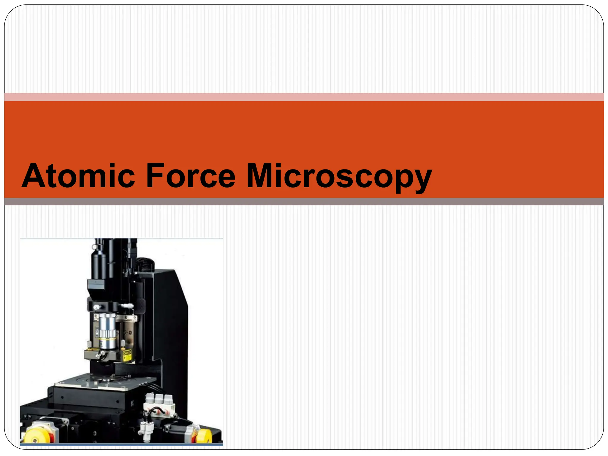
Atomic Force Microscopy
 Atomic force microscopy (AFM) is a very-high-
resolution type of scanning probe
microscopy(SPM), with high resolution on the order
of fractions of a nanometer, more than 1000 times
better than the optical microscopy.
 The information is gathered by "feeling" or
"touching" the surface with a mechanical probe.
Background and History
 1981 – Swiss scientists Gerd Binnig
and Heinrich Rohrer- Atomic
resolution microscopy,
 simple
 1986 – Nobel prize
General Applications
1
Materials
Investigated: Thin
and thick film
coatings,
ceramics,
composites,
glasses, synthetic
and biological
membranes,
metals, polymers,
and
semiconductors.
3
AFM can image
surface of
material in
Nano
resolution and
also measure
force at the
nano- scale.
2
Used to study
phenomena of:
Abrasion,
corrosion,
etching (scratch),
friction,
lubricating,
plating, and
polishing.
Further Applications
Parts of AFM
1. Laser (Illumination)– deflected
off cantilever
2. Mirror –reflects laser beam to
photo detector
3. Photo detector –dual element
photodiode that measures
differences in light intensity and
converts to voltage
4. Amplifier- amplifies the signal
5. Recorder
6. Sample
7. Probe –tip that scans sample
made of Si
8.Cantilever –moves as scanned
over sample and deflects laser beam
Principle
 The AFM consists of a cantilever with a sharp tip (probe) at its end that is
used to scan the specimen surface.
 The cantilever is typically silicon or silicon nitride with a tip radius of
curvature on the order of nanometers.
 When the tip is brought into proximity of a sample surface, laser beam
activates the forces between the tip and the sample lead to a deflection of
the cantilever.
 Depending on the situation, forces that are measured in AFM include
mechanical contact force, van der Waals forces, capillary forces, chemical
bonding, electrostatic forces.
8
How Does AFM Work?
Scanners
 AFM scanners are made
from piezoelectric material, which expands and
contracts proportionally to an applied voltage.
 Peizo electric material- Barium titanate,
Zirconium titanate
 Whether they elongate or contract depends upon
the voltage applied.
 Traditionally the tip or sample is mounted on a
'tripod' of three piezo crystals, with each
responsible for scanning in
the x,y and z directions.
 Because of differences in material or size, the
sensitivity varies from scanner to scanner.
Experimental Procedures
Sample preparation
Thin layer of wax on steel disk Measuring
3-D Imaging
Manipulating/Analyzing
Diagram
Measuring
-3 D
Imaging
Analysing
Scanning the Sample/measure
 Tip brought within
nanometers of the sample
(Van der Waals)
 Radius of tip limits the
accuracy of analysis/
resolution
 Stiffer cantilevers protect
against sample damage
because they deflect less in
response to a small force
Data Analysis
Morphology Characterization/
Sub microscopic level
Surface roughness
quantification
Physical properties/
Swelling, cohesiveness,
smoothness
Will be
analyzed
AFMTips
FIB- Focused ion beam
THREE Modes: Contact mode,
Non-contact, mode, Tapping Mode
A.Contact Mode; hard, stable samples in air or liquid
B. Non-Contact Mode: non- invasive sampling.
C. Tapping (Intermittent contact): No shear and damaging samples
A. Contact
Mode
Measures repulsion between tip and sample
Force of tip against sample remains constant
Problems: excessive tracking forces
applied by probe to sample- sample will destroy.
B. Non-Contact Mode
Measures attractive forces between tip and sample
Tip doesn’t touch sample
Van der Waals forces between tip and sample detected
Problems: Can’t use with samples in fluid
Used to analyze semiconductors
Doesn’t degrade or interfere with sample- better for
soft samples
C. Tapping (Intermittent- Contact)
Mode
Tip vertically oscillates between contacting sample
surface and lifting of at frequency of 50,000 to
500,000 cycles/sec.
Oscillation amplitude reduced as probe contacts
surface due to loss of energy caused by tip
contacting surface
Advantages: overcomes problems associated with
friction, adhesion, electrostatic forces
More effective for larger scan sizes
Advantages and Disadvanteges
of AFM
In general
The future of AFM
 Sharper tips by improved micro-fabrication
processes: (tip – sample interaction tends to
distort or destroy soft biological molecules )
 development of more flexible cantilever
springs and less damaging and non-sticky
probes needed
Nano-Identification on Fiber surface
MMF
Viscose
Rayon
Cotton

Atomic force microscopy for food applications

  • 1.
  • 2.
     Atomic forcemicroscopy (AFM) is a very-high- resolution type of scanning probe microscopy(SPM), with high resolution on the order of fractions of a nanometer, more than 1000 times better than the optical microscopy.  The information is gathered by "feeling" or "touching" the surface with a mechanical probe.
  • 3.
    Background and History 1981 – Swiss scientists Gerd Binnig and Heinrich Rohrer- Atomic resolution microscopy,  simple  1986 – Nobel prize
  • 4.
    General Applications 1 Materials Investigated: Thin andthick film coatings, ceramics, composites, glasses, synthetic and biological membranes, metals, polymers, and semiconductors. 3 AFM can image surface of material in Nano resolution and also measure force at the nano- scale. 2 Used to study phenomena of: Abrasion, corrosion, etching (scratch), friction, lubricating, plating, and polishing.
  • 5.
  • 6.
    Parts of AFM 1.Laser (Illumination)– deflected off cantilever 2. Mirror –reflects laser beam to photo detector 3. Photo detector –dual element photodiode that measures differences in light intensity and converts to voltage 4. Amplifier- amplifies the signal 5. Recorder 6. Sample 7. Probe –tip that scans sample made of Si 8.Cantilever –moves as scanned over sample and deflects laser beam
  • 8.
    Principle  The AFMconsists of a cantilever with a sharp tip (probe) at its end that is used to scan the specimen surface.  The cantilever is typically silicon or silicon nitride with a tip radius of curvature on the order of nanometers.  When the tip is brought into proximity of a sample surface, laser beam activates the forces between the tip and the sample lead to a deflection of the cantilever.  Depending on the situation, forces that are measured in AFM include mechanical contact force, van der Waals forces, capillary forces, chemical bonding, electrostatic forces. 8
  • 9.
  • 11.
    Scanners  AFM scannersare made from piezoelectric material, which expands and contracts proportionally to an applied voltage.  Peizo electric material- Barium titanate, Zirconium titanate  Whether they elongate or contract depends upon the voltage applied.  Traditionally the tip or sample is mounted on a 'tripod' of three piezo crystals, with each responsible for scanning in the x,y and z directions.  Because of differences in material or size, the sensitivity varies from scanner to scanner.
  • 12.
    Experimental Procedures Sample preparation Thinlayer of wax on steel disk Measuring 3-D Imaging Manipulating/Analyzing
  • 13.
  • 14.
    Scanning the Sample/measure Tip brought within nanometers of the sample (Van der Waals)  Radius of tip limits the accuracy of analysis/ resolution  Stiffer cantilevers protect against sample damage because they deflect less in response to a small force
  • 15.
    Data Analysis Morphology Characterization/ Submicroscopic level Surface roughness quantification Physical properties/ Swelling, cohesiveness, smoothness Will be analyzed
  • 16.
  • 17.
    THREE Modes: Contactmode, Non-contact, mode, Tapping Mode A.Contact Mode; hard, stable samples in air or liquid B. Non-Contact Mode: non- invasive sampling. C. Tapping (Intermittent contact): No shear and damaging samples
  • 18.
    A. Contact Mode Measures repulsionbetween tip and sample Force of tip against sample remains constant Problems: excessive tracking forces applied by probe to sample- sample will destroy.
  • 19.
    B. Non-Contact Mode Measuresattractive forces between tip and sample Tip doesn’t touch sample Van der Waals forces between tip and sample detected Problems: Can’t use with samples in fluid Used to analyze semiconductors Doesn’t degrade or interfere with sample- better for soft samples
  • 20.
    C. Tapping (Intermittent-Contact) Mode Tip vertically oscillates between contacting sample surface and lifting of at frequency of 50,000 to 500,000 cycles/sec. Oscillation amplitude reduced as probe contacts surface due to loss of energy caused by tip contacting surface Advantages: overcomes problems associated with friction, adhesion, electrostatic forces More effective for larger scan sizes
  • 22.
  • 23.
  • 24.
    The future ofAFM  Sharper tips by improved micro-fabrication processes: (tip – sample interaction tends to distort or destroy soft biological molecules )  development of more flexible cantilever springs and less damaging and non-sticky probes needed
  • 25.
    Nano-Identification on Fibersurface MMF Viscose Rayon Cotton