1. AIM : To design a voltage regulated power supply using an op-amp with
an inbuilt overload protection.
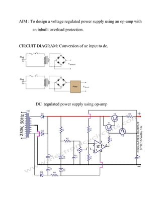
CIRCUIT DIAGRAM: Conversion of ac input to dc.
DC regulated power supply using op-amp
3. D5 6.8V 500mA Zener Diode
T1 2N1481 or D313 or 2SC1061
T2 2N3055
T3 BC107
IC1 LM741
TR1 SEC 15V, 2AMP
BASIC OP-AMP :
4. THEORY:
The function of a voltage regulator is to provide a
stable dc voltage for powering of other electronic circuits. A voltage
regulator is capable of providing substantial output current.
Rectifier diodes D1 and D2 along with capacitor C1 provide the
main unregulated supply. D3, C2, R8 and zener diode provide a negative
voltage supply for the 741. The non-inverting input terminal of 741 is
given a stable voltage by R3 which is the control to set the output. A
fraction of the regulated output is fed back via R4 and R5 to the
inverting input terminal. The operational amplifier adjusts its output
voltage so as to keep the voltage at the input terminals equal. Thus the
output gets regulated. The output of 741 is amplified by a compound
emitter follower T1 and T2.
All the current flows through R6. If the load current exceeds 1A, the
voltage drop across R6 exceeds 0.6 volts and T3 starts conducting. This
bypasses the supply to T1 and T2 and the regulating action stops. The
output voltage therefore starts falling when the load current exceeds 1A.
Any of the output terminals can be grounded to get a positive or a
negative voltage with respect to the ground.
A 100ohm ¼ w resistance is added in the base
circuit of current limiting transistor T3,to protect it during an output
dead short,with out which the junction transistor will blow out.
The voltage regulated power supply provides
adjustable voltage output at a load current up to 1A. The supply has
built in overload protection.