SlideShare a Scribd company logo
1 of 11
Download to read offline
ORGANIC LIGHT EMITTING DIODE


ORGANIC LIGHT EMITTING DIODE
OLED:                                                             The LC material is inherently a transparent
                                                            material, but it has a property where its optical
        OLED’s are simple solid-state devices
                                                            axis can be rotated by applying an electric field
(more of an LED) comprised of very thin films of
                                                            across the material.
organic compounds in the electro-luminescent
layer. These organic compounds have a special
property of creating light when electricity is
applied to it. The organic compounds are
designed to be in between two electrodes. Out of


                                                                    FIGURE 2: WORKING OF LCD

                                                                  When the LC material optical axis is made
                                                            to align with the two polarizers’ axis, light will
                                                            pass through the second polarizer. On the other
                                                            hand, if the optical axis is rotated 90 degrees,
                                                            light will be polarized by the first polarizer,
                                                            rotated by the LC material and blocked by the
these one of the electrodes should be transparent.          second polarizer.
                FIGURE 1: OLED                              LIMITATIONS OF LCD:
They have been developed for applications in flat                  The polarizers and the LC material absorb
panel displays that provide visual imagery which            light. On a typical monochrome LCD display the
is easy to read, vibrant in colors and less                 polarizers alone absorb 50% of the incident light.
consuming of power.                                         On an active matrix displayTFT layer, the light
                                                            throughput may be as low as 5% of the incident
LCD:
                                                            light. Such low light output efficiency requires
LCD is a non-emissive display device. This                  with a LC based displays to have a powerful
means that they do not emit light on their own.             backside or ambient light illumination to achieve
Thus, an LCD operates on the basis of either                sufficient brightness. This causes LCD’s to be
passing or blocking light that is produced by an            bulky and power hungry.The LC cells are in front
external light Source. Applying an electric field           are relatively thin and their operation relatively
across an LCD cell controls its transparency or             power efficient. It is the backside light that takes
reflectivity. A cell blocking (absorbing) light will        up most space as well as power. In fact with the
thus be seen as black and a cell passing                    advent of low power microprocessors, the LCD
(reflecting) light will be seen as white. For a color       module is the primary cause of short battery life
displays, there are color filters added in front of         in notebook computers.
each of the cells and a single pixel is represented
by three cells, each responsible for the basic                     Moreover, the optical properties of the LC
colors: red, green and blue.                                material and the polarizer also causes what is
            The basic physical structure of a LCD           known as the viewing angle effect. The effect is
cell is shown in figure2.The liquid crystal (LC)            such that when a user is not directly in front of
material is sandwiched between two polarizers               the display, the image can disappear or sometime
and two glass plates (or between one glass plate            seem to invert (dark images become light and
                                                            light images become dark).
and one Thin Film Transistor (TFT) layers).The
polarizers are integral to the working of the cell.
                                                        1
ORGANIC LIGHT EMITTING DIODE


EVOLUTION OF OLED:                                              For an Organic LED, organic layer
                                                         corresponding to the p-type material is called the
       The discovery of the electroluminescence
                                                         hole-transport layer (HTL) and similarly the layer
property in organic materials in 1950s is
                                                         corresponding to the n-type material is called the
considered to be the stepping stone of OLED.
                                                         electron-transport layer (ETL). In Figure 3, Alq3
                                                         is the ETL and TPD is the HTL.
        Later in 1960, a scientist called Martin
Pope discovered an ohmic, dark injecting                       Similar to doped silicon, when ETL and
electrode contact to organic nature of crystals.         HTL materials are placed to create a junction, the
With this he was also able to explain the work           energy bands equilibrates to maintain continuity
functions for both the holes and electrons while         across the structure. When a potential difference
injecting electrode contacts. These dark injecting       is applied across the structure, a drift current
holes and electrons formed to be the base for an         flows through the structure. The injected carries
OLED device. The technique was further                   recombination at the junction consists of both
experimented with DC electroluminescence under           thermal and optical recombination, which emits
different conditions. Later it was found that            photons.
electroluminescent materials can also act as
doped insulators. Thus came the discovery of a
double injection induced OLED device.

The first proper OLED was manufactured in 1980
by Dr.Ching W Tang and Steven Van Slyke. The
OLED had a double layer structure. When the
holes and electrons were transported separately
and when combined together produced a light in                               FIGURE 4:
the organic layer centre. This light was produced               OPTICAL RECOMBINATION IN OLED
at a very low operating voltage with high
                                                         Figure 4 shows optical recombination from the
efficiency.
                                                         energy band perspective. Note that LUMO is a
Now more research is being done with the
                                                         short form for Lowest Unoccupied Molecular
application of OLED on polymer so as to obtain a
                                                         Orbital, which corresponds to the conduction
higher efficiency OLED.
                                                         band in the energy diagram of doped silicon, and
ORGANIC LED STRUCTURE:
                                                         HOMO is a short form for Highest Occupied
The p-n junction of oled is made from an organic         Molecular Orbital, which corresponds to the
compound such as: Alq3 (Aluminum tris (8-                valence band in the energy diagram of doped
hydroxyquinoline)) and diamine (TPD). The                silicon.
molecular structure of some typical organic
                                                         Since an OLED emits light through a
materials used are shown.
                                                         recombination process, it does not suffer from the
                                                         viewing angle limitation like an LC based device.
                                                         Note that for any device to become a viable
                                                         candidate for use in flat panel displays it has to be
                                                         able to demonstrate high brightness, good power
                                                         efficiency, good color saturation and sufficient
                                                         lifetime. Reasonable lower limits specifications
                                                         for any candidate device should include the
                                                         following: brightness of ~ 100cd/m 2operating
FIGURE 3: MOLECULAR STRUCTURE OF
                                                         voltage of 5-15V.
ORGANIC MATERIALS

                                                     2
ORGANIC LIGHT EMITTING DIODE


COMPONENTS IN AN OLED:                                               The substrate is used to support the
                                                             OLED. The anode is used to inject more holes
The components in an OLED differ according to
                                                             when there is a path of current. The conducting
the number of layers of the organic material.
                                                             layer is used to carry the holes from the anode.
There is a basic single layer OLED, two layer and
also three layer OLED’s. As the number of layers             The cathode is used to produce electrons when
increase the efficiency of the device also                   current flows through its path. The emissive layer
increases. The increase in layers also helps in              is the section where the light is produced. This
injecting charges at the electrodes and thus helps           layer is used to carry the electrons form the
in blocking a charge from being dumped after                 cathode.
reaching the opposite electrode.
Any type of OLED consists of the following                   WORKING OF OLED:
components.Emissive layer, Conducting layer,                        Before going on to the detailed
Substrate, Anode and Cathode terminals.                      explanation of its working, it is important to
                                                             know how the emissive layers and conducting
                                                             layers are added to the substrate. There are
                                                             mainly three basic methods for this operation.
                                                             They are:-

                                                             Inkjet Printing Technique – This is the cheapest
                                                             and most commonly used technique. The method
                                                             is same as the paper printing mechanism where
                                                             the organic layers are sprayed onto the substrates.
   FIGURE 5: COMPONENTS OF OLED                              This method is also highly efficient and they can
As the emissive layer and the conducting layer is            be used for printing very large displays like
made up of organic molecules (both being                     billboards and also big TV screens.
different), OLED is considered to be an organic
semi-conductor, and hence its name. The organic              Organic Vapour Phase Deposition (OVPD) – This
molecules have the property of conducting                    is also an efficient technique which can be carried
electricity and their conducting levels can be               out at a low cost. A cooled substrate is being hit
varied form that of an insulator to a conductor.             by the organic molecules, which was evaporated
                                                             in a low pressure, high temperature chamber. The
The emissive layer used in an OLED is made up
of organic plastic molecules, out of which the               gas is carried onto the substrate with the help of a
most commonly used is polyfluorene. The                      carrier gas.
conducting layer is also an organic molecule, and
the commonly used component is polyaniline.The               Vacuum Thermal Evaporation (VTE)-This
substrate most commonly used may be a plastic,               method is also commonly known as vacuum
foil or even glass.The anode component should                deposition method. This operation is carried out
be transparent. Usually indium tin oxide is used.            by gently heating the organic molecules so that
This material is transparent to visible light. It also       they evaporate and subside on the substrates. As
has a great work function which helps in injecting           the heating method is complicated and the
holes into the different layers. The cathode                 strictness of parameters should be highly
component depends on the type of OLED                        accurate, this method is economical as well.
required. Even a transparent cathode can be used.            After the organic material has been applied to the
Usually metals like calcium and aluminium used
                                                             substrate the real working of the OLED begins.
because they have lesser work functions than
                                                             OLEDs emit light in a similar manner to LEDs,
anodes which helps in injecting electrons into the
                                                             through a process called electrophosphorescence
different layers.


                                                         3
ORGANIC LIGHT EMITTING DIODE


       The battery or power supply of the device
containing the OLED applies a voltage across the
OLED.


1. Cathode (−), 2. Emissive Layer, 3. Emission                    FIGURE 7: VARIATION OF I-V
of radiation, 4. Conductive Layer, 5. Anode (+)             CHARACTERISTIC WITH TEMPERATURE
       FIGURE 6: WORKING OF OLED                                  Besides temperature, the I-V characteristic
        Electrical current flows from the cathode          also depends strongly on the type of
to the anode through the organic layers (an                anode/cathode used in the device as well as the
electrical current is a flow of electrons). The            thickness of the organic active Electro
cathode gives electrons to the emissive layer of           Luminescence (EL) layer. The particular Figure
organic molecules.The anode removes electrons              shows the I-V characteristic variation with the
from the conductive layer of organic molecules.            thickness of the organic layer.
(This is the equivalent to giving electron holes to
the conductive layer). At the boundary between
the emissive and the conductive layers, electrons
find electron holes. When an electron finds an
electron hole, the electron fills the hole (it falls
into an energy level of the atom that is missing an
electron). When this happens, the electron gives
up energy in the form of a photon of light. The
OLED emits light.                                                 FIGURE 8: VARIATION OF I-V
        The color of the light depends on the type             CHARACTERISTIC WITH THICKNESS
of organic molecule in the emissive layer.
Manufacturers place several types of organic               MODERN TECHNOLOGIES IN OLED’S
films on the same OLED to make color displays.             (1)High Efficiency Materials:
The intensity or brightness of the light depends                       These materials emit light through
on the amount of electrical current applied. The            the process of electrophosphorescence. In
more the current, the brighter the light.                   traditional OLEDs, the light emission is based
I-V CHARACTERISTIC VARIATION:                               on fluorescence, a transition from a singlet
        The I-V characteristics of OLED is also             excited state of a material. According to
varying with time. Several factors contribute to            theoretical and experimental estimation, the
the I-V characteristic variation. The first and             upper limit of efficiency of an OLED doped
foremost is temperature. The I-V characteristic             with fluorescent material, is approximately
depends quite strongly on the operating                     25%.
temperature. The I-V characteristic variation pose                  With our electro phosphorescent
a challenge to the control of OLED based                    materials used as a dopant, which exploits both
displays as the I-V operating points have to be             singlet and triplet excited states, this upper
shifted depending on the operating temperature as           limit is virtually eliminated. We are equipped
shown in figure 7.                                          with the potential of 100% efficiency.


                                                       4
ORGANIC LIGHT EMITTING DIODE


           We are working towards the                            In an active matrix OLED display
commercialization of electro phosphorescent              (AMOLED), information is sent to the transistor
devices by optimizing the device efficiency,             in each pixel, telling it how bright the pixel
color purity and device storage and operation            should shine. The TFT then stores this
durabilities.                                            information and continuously controls the
                                                         current flowing through the OLED. In this way
                                                         the OLED is operating all the time, avoiding the
                                                         need for the very high currents necessary in a
                                                         passive matrix display.
                                                                 The new high efficiency material systems
                                                         are ideally suited for use in active matrix OLED
                                                         displays, and their high efficiencies should result
                                                         in greatly reduced power consumption.

                                                                 This type of OLED is suitable for high
                                                         resolution and large size display. Though the
                                                         manufacturing process is the same, the anode
       FIGURE 9: TRIPLET EMITTER                         layers have a Thin-film transistor (TFT) plane in
          Such a process is facilitated by the           parallel to it so as to form a matrix. This helps in
development and modification of charge                   switching each pixel to it’s on or off state as
transport materials, charge blocking materials           desired, thus forming an image. This is the least
and luminescent materials, and their                     power consuming type among others and also has
incorporation into devices. In addition to the           quicker refresh rates which makes them suitable
fabrication of high quality devices, UDC is also         for video as well.
committed to a high standard of device testing.
                                                         (3)Passive Matrix OLED (PMOLED):
Our scientists and engineers have custom
developed sophisticated test hardware and                       Passive Matrix displays consist of an
software for this purpose.                               array of picture elements, or pixels, deposited on
(2)Active Matrix OLED (AMOLED):                          a patterned substrate in a matrix of rows and
                                                         columns.
            In an active matrix display, the array
is still divided into a series of row and column
lines, with each pixel formed at the intersection
of a row and column line. However, each pixel
now consists of an organic light emitting diode
(OLED) in series with a thin film transistor
(TFT). The TFT is a switch that can control the
amount of current flowing through the OLED.


                                                                      FIGURE 11: PMOLED
                                                                 In an OLED display, each pixel is an
                                                         organic light emitting diode, formed at the
                                                         intersection of each column and row line. The
                                                         first OLED displays, like the first LCD, are
                                                         addressed as a passive matrix. This means that to
                                                         illuminate any particular pixel, electrical signals
            FIGURE 10: AMOLED                            are applied to the row line and column line (the
                                                         intersection of which defines the pixel).
                                                     5
ORGANIC LIGHT EMITTING DIODE


        The more current pumped through each                    FOLEDs are organic light emitting devices
pixel diode, the brighter the pixel looks to our          built on flexible substrates. Flat panel displays
eyes.The design of this type of OLED makes                have traditionally been fabricated on glass
them more suitable for small screen devices like          substrates because of structural and/or processing
cell phones, MP3 players and so on. Though this           constraints. Flexible materials have significant
type is less power consuming than an LCD and              performance advantages over traditional glass
LED (even if connected to other external                  substrates.
circuitry’s), it is the most power consuming
                                                           FOLEDs Offer Revolutionary Features for
comparative to other OLED’s.
                                                           Displays:
        This type is very easy to make as strips of        (i)Flexibility: For the first time, FOLEDs may
anode and cathode are kept perpendicular to each           be made on a wide variety of substrates that
other. When they are both intersected light is             range from optically-clear plastic films to
produced. As there are strips of anode and                 reflective metal foils. These materials provide
cathode, current is applied to the selected strips         the ability to conform, bend or roll a display
and is applied to them. This helps in determining          into any shape. This means that a FOLED
the on or off pixels.                                      display may be laminated onto a helmet face
                                                           shield, a military uniform shirtsleeve, an
(4)Inverted OLED:
                                                           aircraft cockpit instrument panel or an
                                                           automotive windshield.

                                                           (ii)Ultra-lightweight, thin form: The use of thin
                                                           plastic substrates will also significantly reduce
                                                           the weight of flat panel displays in cell phones,
                                                           portable computers and, especially, large-area
                                                           televisions-on-the-wall. For example, the
                                                           weight of a display in a laptop may be
                                                           significantly reduced by using FOLED
       FIGURE 12: INVERTED OLED                            technology.

       This type uses a bottom cathode, which is
                                                           (iii)Durability: FOLEDs will also generally be
connected to the drain end of an n-channel TFT
                                                           less breakable, more impact resistant and more
backplane. This method is usually used for
                                                           durable compared to their glass-based
producing low cost OLED with little applications.
                                                           counterpart.
(5)Foldable OLED (FOLED):                                  (iv)Cost-effective processing: OLEDs are
                                                           projected to have full-production level cost
                                                           advantage over most flat panel displays. With
                                                           the advent of FOLED technology, the prospect
                                                           of roll-to-roll processing is created. To this end,
                                                           our research partners have demonstrated a
                                                           continuous organic vapor phase deposition
                                                           (OVPD) process for large-area roll-to-roll
                                                           OLED processing. While continuous web
                                                           FOLED         processing       requires     further
                                                           development, this process may provide the
       FIGURE 13: FOLDABLE OLED                            basis for very low-cost, mass production.


                                                      6
ORGANIC LIGHT EMITTING DIODE


      This type is mainly used in devices which
have more chance of breaking. As this material is
strong it reduces breakage and therefore is used in
cell phones, computer chips, GPS devices and
PDA’s. They are also flexible, durable and
lightweight. As its name explains, these OLED’s
are foldable and can also be connected to clothes.
They use different types of substrates like flexible
metallic foils, plastics and so on.

(6)Top Emitting OLED:
        This type of OLED is integrated with a
transistor backplane that is not transparent. Such
devices are suitable for matrix applications like                FIGURE 15: TRANSPARENT OLED
smart cards. The substrate used for this device is
                                                                   This device has a good contrast even in
of the opaque/reflective type. As a transparent
                                                           bright sunlight so it is applicable in head-up
substrate is used the electrode used is either semi-
                                                           displays, mobile phones, smart windows and so
transparent or fully transparent. Otherwise the
                                                           on. In this device, the entire anode, cathode and
light will not pass through the transparent
                                                           the substrate are transparent. When they are in the
substrate.
                                                           off position, they become almost completely
                                                           transparent as their substrate. This type of OLED
                                                           can be included in both the active and passive
                                                           matrix categories. As they have transparent
                                                           parameters on both the sides, they can create
                                                           displays that are top as well as bottom emitting.

                                                           (8)White OLED:
                                                                   White OLEDs emit white light that is
                                                           brighter, more uniform and more energy efficient
                                                           than that emitted by fluorescent lights. White
     FIGURE 14: TOP EMITTING OLED                          OLEDs also have the true-color qualities
(7)Transparent OLED:                                       of incandescent lighting. Because OLEDs can be
                                                           made in large sheets, they can replace fluorescent
        The Transparent OLED (TOLED) uses a                lights that are currently used in homes and
proprietary transparent contact to create displays         buildings. Their use could potentially reduce
that can be made to be top-only emitting, bottom-          energy costs for lighting.
only emitting, or both top and bottom emitting
(transparent). TOLEDs can greatly improve
contrast, making it much easier to view displays
in bright sunlight. Because TOLEDs are 70%
transparent when turned off, they may be
integrated into car windshields, architectural
windows, and eyewear. Their transparency
enables TOLEDs to be used with metal, foils,
silicon wafers and other opaque substrates for                    FIGURE 16: WHITE OLED
top-emitting devices.

                                                       7
ORGANIC LIGHT EMITTING DIODE


      This device creates the brightest light of all.             This device uses the composite colours as
They are manufactured in large sheets. Thus they            sub pixels and also on top of each other. This
can easily replace fluorescent lamps. They are              causes the reduction in pixel gap and also an
also cost-effective and also consumes less power.           increase in colour depth. Thus they are being
(9)Stacked OLED (SOLED):                                    introduced as television displays.

      The Stacked OLED (SOLED) uses                         (10)ORGANIC LASERS:
 Universal Display Corporation's award-
                                                                        An organic laser is a solid-state
 winning, novel pixel architecture that is based
                                                             device based on organic materials and
 on stacking the red, green, and blue subpixels
                                                             structures similar to those used in UDC's
 on top of one another instead of next to one
                                                             display technologies. An optically-pumped
 another as is commonly done in CRTs and
                                                             organic laser demonstrates five key laser
 LCDs. This improves display resolution up to
                                                             characteristics: spatial coherence, a clear
 three-fold and enhances full-color quality.
                                                             threshold, strongly polarized light emission,
 SOLEDs may provide the high resolution
                                                             spectral line narrowing, and the existence of
 needed      for    wireless    worldwide-web
                                                             laser cavity modes. To realize commercial
 applications.
                                                             potential, the key technical challenge today is
                                                             to demonstrate a mechanism for the electrical
                                                             pumping of these lasers.
                                                                        The use of small-molecule organic
                                                             materials opens the door to an entirely new
                                                             class of light emitters for diode lasers. These
                                                             organic lasers may offer:
                                                             a) Greater color variety
                                                             b) Tunability
                                                             c) Further miniaturization
         FIGURE 17: STACKED OLED
                                                             d) Easier processing
 SOLED DISPLAY:
                                                             e) Lower cost in a host of end uses
             A SOLED display consists of an
                                                            ORGANIC VAPOUR PHASE DEPOSITION:
 array of vertically-stacked TOLED sub-pixels.
 To separately tune color and brightness, each                          The OVPD production process
 of the red, green and blue (R-G-B) sub-pixel                utilizes a carrier gas stream in a hot walled
 elements is individually controlled. By                     reactor at very low pressure to precisely deposit
 adjusting the ratio of currents in the three                the thin layers of organic materials used in
 elements, color is tuned. By varying the total              OLED        displays.   Conventional      OLED
 current through the stack, brightness is varied.            fabrication equipment evaporates the organic
 By modulating the pulse width, gray scale is                molecules at high temperature and pressure.
 achieved. With this SOLED architecture, each                OVPD offers the ability to precisely control the
 pixel can, in principle, provide full color.                multi-source deposition required for full-color
 Universal Display Corporation's SOLED                       OLED displays. The OVPD design should also
 technology may be the first demonstration of                be adaptable to the rapid, uniform deposition of
 an vertically-integrated structure where                    organics on large-area substrates and for roll-
 intensity, color and gray scale can be                      to-roll processing. The technology, Organic
 independently tuned to achieve high-resolution              Vapour Phase Deposition can enable low cost,
 full-color.                                                 precise, high throughput process for fabricating
                                                             OLEDs.


                                                        8
ORGANIC LIGHT EMITTING DIODE


ADVANTAGES OF OLED:                                         7.Efficient in Energy: OLED displays consumes
                                                            less energy as compared to LCD displays and
      The different manufacturing process of                other display screens. No backlight is required in
OLEDs lends itself to several advantages over               these screens which is the biggest OLED
flat-panel displays made with LCD technology.               advantage for use in portable gadgets.

1. Lower cost in the future: OLEDs can be                   8.Good for Eyes: Another great advantage of
printed onto any suitable substrate by an inkjet            OLED is that it pts less stains on eyes and hence
printer or even by screen printing,[52] theoretically       are eye soothening. These screens provide better
making them cheaper to produce than LCD or                  viewing experience because they have better
plasma displays. However, fabrication of the                contrast, brightness and color aspects.
OLED substrate is more costly than that of a TFT
LCD, until mass production methods lower cost               9.Self luminous: The OLED is self luminous i.e.
through scalability.                                        it creates the required light energy on its own. It
                                                            does not require any external source for creating
2. Light weight & flexible plastic substrates:              light like LCD.
OLED displays can be fabricated on flexible
plastic substrates leading to the possibility of            10.Environmental drawbacks: There are no
Organic light-emitting diode roll-up display being          environmental drawbacks while using OLED as it
fabricated or other new applications such as roll-          uses organic materials.
up displays embedded in fabrics or clothing. As
the substrate used can be flexible such as PET,             11.Power in-take: OLED does not require any
the displays may be produced inexpensively.                 power in take when turned off.

3. Wider viewing angles & improved                          12.Durability: Another great advantage of OLED
brightness: OLEDs can enable a greater artificial           is that it is more durable than traditional screens.
contrast ratio (both dynamic range and static,              There chance of getting broken is comparitively
measured in purely dark conditions) and viewing             less to LCD screens and other displays.
angle compared to LCDs because OLED pixels
directly emit light. OLED pixel colours appear              DISADVANTAGES OF OLED:
correct and unshifted, even as the viewing angle
approaches 90 degrees from normal.                          1.Lifespan: The biggest technical problem for
                                                            OLEDs was the limited lifetime of the organic
4. Better power efficiency: LCDs filter the light           materials. In particular, blue OLEDs historically
emitted from a backlight, allowing a small                  have had a lifetime of around 14,000 hours to half
fraction of light through so they cannot show true          original brightness (five years at 8 hours a day)
black, while an inactive OLED element does not              when used for flat-panel displays. This is lower
produce light or consume power.                             than the typical lifetime of LCD, LED or PDP
                                                            technology—each currently rated for about
5. Response time: OLEDs can also have a faster              25,000 - 40,000 hours to half brightness,
response time than standard LCD screens.                    depending on manufacturer and model.
Whereas LCD displays are capable of a 1 ms
response time or less offering a frame rate of              2.Color balance issues: Additionally, as the
1,000 Hz or higher, an OLED can theoretically               OLED material used to produce blue light
                                                            degrades significantly more rapidly than the
have less than 0.01 ms response time enabling               materials that produce other colors, blue light
100,000 Hz refresh rates.                                   output will decrease relative to the other colors of
                                                            light. This differential color output change will
6.Slimmer: The biggest adavantage of OLED                   change the color balance of the display and is
screen is that it is slimmer than LCD display.              much more noticeable than a decrease in overall
While LCD and Plasma displays could be few                  luminance. This can be partially avoided by
inches thick, OLED advantage is that it is only             adjusting colour balance but this may require
few millimeters thick.                                      advanced control circuits.

                                                        9
ORGANIC LIGHT EMITTING DIODE


3.Efficiency of blue OLEDs: Improvements to
the efficiency and lifetime of blue OLEDs is vital
to the success of OLEDs as replacements for
LCD technology. Considerable research has been
invested in developing blue OLEDs with high
external quantum efficiency as well as a deeper
blue color.

4.Water damage: Water can damage the organic
materials of the displays. Therefore, improved
sealing processes are important for practical
                                                                    FIGURE 18: MOBILE WITH OLED
manufacturing. Water damage may especially
                                                                               DISPLAY
limit the longevity of more flexible displays.
                                                             16) Smart   goggles/helmets for scuba divers,
5.UV sensitivity: OLED displays can be                           motorcycle riders
damaged by prolonged exposure to UV light.                   17) Medical test equipment
PRODUCT CONCEPTS                                             18) Wide area, full-motion video camcorders
      Universal Display Corporation has only                 19) Global positioning systems (GPS)
begun to imagine what our OLED technology                    20) Integrated computer displaying eyewear
can create in the way of products for our world              21) Rugged military portable communication
and our future. The technology has the potential                 devices
to not only improve existing products, but also              ORGANIC FUTURE
to create exciting, new product possibilities, for                   The first products using organic displays
example:                                                     are already being introduced into the market
1) Low-power, bright, colorful cell phones                   place. And while it is always difficult to predict
2) Full      color,    high-resolution,     personal         when and what future products will be
    communicators                                            introduced, many manufacturers are now
3) Wrist-mounted, featherweight, rugged PDAs                 working to introduce cell phones and personal
4) Wearable, form-fitting, electronic displays               digital assistants with OLED displays within the
5) Full-color, high resolution, portable Internet            next one or two years. The ultimate goal of
    devices and palm size computers                          using high-efficiency, phosphorescence, flexible
6) High-contrast automotive instrument and                   OLED displays in lap top computers and even
    windshield displays                                      for home video applications may be no more
7) Heads-up instrumentation for aircraft and                 than a few years into future.
    automobiles
8) Automobile light systems without bulbs
9) Flexible, lightweight, thin, durable, and
    highly efficient laptop screens
10) Roll-up,       electronic,     daily-refreshable
    newspaper
11) Ultra-lightweight,      wall-size      television
    monitor
12) Office windows, walls and partitions that                 FIGURE 19: IDENTITY CARD WITH OLED
    double as computer screens                                              DISPLAY
13) Color-changing lighting panels and light                        However, there remains much to be done
    walls for home and office                                if organics are to establish a foothold in the
14) Low-cost organic lasers                                  display market. Achieving higher efficiencies,
15) Computer-controlled, electronic shelf pricing            lower operating voltages, and lower device life
    for supermarkets and retail stores                       times are all challenges still to be met.
                                                        10
ORGANIC LIGHT EMITTING DIODE


        Given the aggressive worldwide efforts           REFERENCES:
in this area, emissive organic thin films have an          1. "Brief OLED history". Comboled Project
excellent chance of becoming the technology of              2.   "Organic    electroluminescent   diodes".
choice for the next generation of high-
                                                                 Applied Physics Letters
resolution, high-efficiency flat panel displays.
                                                            3. Electronic processes in organic crystals
                                                                 and polymers, 2nd ed., by M. Pope
                                                            4. Wikipedia.com


          FIGURE 20: OLED DISPLAY
        In addition to displays, there are many
other opportunities for application of organic
thin-film semiconductors, but to date these have
remained largely untapped. Recent results in
organic electronic technology that may soon find
commercial outlets in display black planes and
other low-cost electronics.


  FIGURE 21: WATCH WITH OLED DISPLAY

CONCLUSION:
       OLEDs offer many advantages over both
LEDs and LCDs. They are thinner, lighter and
more flexible than the crystalline layers in an
LED or LCD. They have large fields of view as
they produce their own light.
       Research and development in the field of
OLEDs is proceeding rapidly and may lead to
future applications in heads up displays,
automotive dash boards, billboard type displays
etc. Because OLEDs refresh faster than LCDs, a
device with OLED display could change
information almost in real time. Video images
could be much more realistic and constantly
updated.

                                                    11

More Related Content

What's hot

Light emiting polymer
Light emiting polymerLight emiting polymer
Light emiting polymerC Jais
 
Light Emitting Diode(LED)
Light Emitting Diode(LED)Light Emitting Diode(LED)
Light Emitting Diode(LED)Naseer LoneRider
 
Led presentation
Led presentationLed presentation
Led presentationAB Amit
 
Light emitting diode’s a Basic Description of LED Bulbs...
Light emitting diode’s a Basic Description of LED Bulbs... Light emitting diode’s a Basic Description of LED Bulbs...
Light emitting diode’s a Basic Description of LED Bulbs... Abhishek Jangid
 
A variable mechanical optical attenuator
A variable mechanical optical attenuatorA variable mechanical optical attenuator
A variable mechanical optical attenuatoromarshehab
 
Light Emitting Diode & OLED
Light Emitting Diode & OLEDLight Emitting Diode & OLED
Light Emitting Diode & OLEDDevansh Gupta
 
light emitting polymers
light emitting polymerslight emitting polymers
light emitting polymersVishnu Mohan
 
MMAE554 Term Paper
MMAE554 Term PaperMMAE554 Term Paper
MMAE554 Term PaperLI HE
 
Flexible oled display technology for electro optical stimulation
Flexible oled display technology for electro optical stimulationFlexible oled display technology for electro optical stimulation
Flexible oled display technology for electro optical stimulationCHINCHU THOMAS
 
Light emittting polymer.ppx
Light emittting polymer.ppxLight emittting polymer.ppx
Light emittting polymer.ppxVineesh Kumar
 
Lightn emitting polymer
Lightn emitting polymerLightn emitting polymer
Lightn emitting polymerMustahid Ali
 
Light cure ppt
Light cure pptLight cure ppt
Light cure pptAyah Sobhy
 
Display technologies
Display technologiesDisplay technologies
Display technologiesSubhajit Das
 

What's hot (20)

Light emiting polymer
Light emiting polymerLight emiting polymer
Light emiting polymer
 
Light Emitting Diode(LED)
Light Emitting Diode(LED)Light Emitting Diode(LED)
Light Emitting Diode(LED)
 
Led presentation
Led presentationLed presentation
Led presentation
 
Anav - led
Anav - ledAnav - led
Anav - led
 
Light emitting Diode
Light emitting DiodeLight emitting Diode
Light emitting Diode
 
Led physics
Led physicsLed physics
Led physics
 
Light emitting diode’s a Basic Description of LED Bulbs...
Light emitting diode’s a Basic Description of LED Bulbs... Light emitting diode’s a Basic Description of LED Bulbs...
Light emitting diode’s a Basic Description of LED Bulbs...
 
Tejpratap
TejpratapTejpratap
Tejpratap
 
A variable mechanical optical attenuator
A variable mechanical optical attenuatorA variable mechanical optical attenuator
A variable mechanical optical attenuator
 
Light Emitting Diode & OLED
Light Emitting Diode & OLEDLight Emitting Diode & OLED
Light Emitting Diode & OLED
 
light emitting polymers
light emitting polymerslight emitting polymers
light emitting polymers
 
MMAE554 Term Paper
MMAE554 Term PaperMMAE554 Term Paper
MMAE554 Term Paper
 
www.edgrep.com
www.edgrep.comwww.edgrep.com
www.edgrep.com
 
Flexible oled display technology for electro optical stimulation
Flexible oled display technology for electro optical stimulationFlexible oled display technology for electro optical stimulation
Flexible oled display technology for electro optical stimulation
 
Led ppt vgec ec engineering
Led ppt vgec ec engineeringLed ppt vgec ec engineering
Led ppt vgec ec engineering
 
Light emittting polymer.ppx
Light emittting polymer.ppxLight emittting polymer.ppx
Light emittting polymer.ppx
 
Lightn emitting polymer
Lightn emitting polymerLightn emitting polymer
Lightn emitting polymer
 
Light cure ppt
Light cure pptLight cure ppt
Light cure ppt
 
Display technologies
Display technologiesDisplay technologies
Display technologies
 
Led (light emitting diode )
Led (light emitting diode )Led (light emitting diode )
Led (light emitting diode )
 

Viewers also liked

Strategies for Optimization of an OLED Device
Strategies for Optimization of an OLED DeviceStrategies for Optimization of an OLED Device
Strategies for Optimization of an OLED DeviceDavid Lee
 
Organic Light Emitting Diode
Organic Light Emitting Diode Organic Light Emitting Diode
Organic Light Emitting Diode Mridul Gupta
 
[Marco mazzeo] organic_light_emitting_diode(book_zz.org)
[Marco mazzeo] organic_light_emitting_diode(book_zz.org)[Marco mazzeo] organic_light_emitting_diode(book_zz.org)
[Marco mazzeo] organic_light_emitting_diode(book_zz.org)bennun78
 
seminar report on night vision technology
seminar report on night vision technologyseminar report on night vision technology
seminar report on night vision technologyAmit Satyam
 
Seminar Report On O.L.E.D.
Seminar Report On O.L.E.D.Seminar Report On O.L.E.D.
Seminar Report On O.L.E.D.Sushant Shankar
 
Oled seminar report
Oled seminar reportOled seminar report
Oled seminar reportMandar Ovarikar
 
OLED technology Seminar Ppt
OLED technology Seminar PptOLED technology Seminar Ppt
OLED technology Seminar PptAshly Liza
 

Viewers also liked (9)

Strategies for Optimization of an OLED Device
Strategies for Optimization of an OLED DeviceStrategies for Optimization of an OLED Device
Strategies for Optimization of an OLED Device
 
Organic Light Emitting Diode
Organic Light Emitting Diode Organic Light Emitting Diode
Organic Light Emitting Diode
 
report on OLEDs
report on OLEDsreport on OLEDs
report on OLEDs
 
[Marco mazzeo] organic_light_emitting_diode(book_zz.org)
[Marco mazzeo] organic_light_emitting_diode(book_zz.org)[Marco mazzeo] organic_light_emitting_diode(book_zz.org)
[Marco mazzeo] organic_light_emitting_diode(book_zz.org)
 
seminar report on night vision technology
seminar report on night vision technologyseminar report on night vision technology
seminar report on night vision technology
 
Seminar Report On O.L.E.D.
Seminar Report On O.L.E.D.Seminar Report On O.L.E.D.
Seminar Report On O.L.E.D.
 
Oled seminar report
Oled seminar reportOled seminar report
Oled seminar report
 
OLED technology Seminar Ppt
OLED technology Seminar PptOLED technology Seminar Ppt
OLED technology Seminar Ppt
 
OLED
OLEDOLED
OLED
 

Similar to OLED: An Efficient Solid-State Lighting Technology

OLED organic light emitting diode
OLED organic light emitting diodeOLED organic light emitting diode
OLED organic light emitting diodeStudent
 
20C35a0411 PPT.pptx
20C35a0411 PPT.pptx20C35a0411 PPT.pptx
20C35a0411 PPT.pptxRohith809769
 
OLED report
OLED reportOLED report
OLED reportKevin Patel
 
Organic light emitting diode (oled)
Organic light emitting diode (oled)Organic light emitting diode (oled)
Organic light emitting diode (oled)AvijitBarua8
 
Electroluminesecnce
ElectroluminesecnceElectroluminesecnce
ElectroluminesecnceSudama04
 
Organic Light Emitting Diodes
Organic Light Emitting DiodesOrganic Light Emitting Diodes
Organic Light Emitting DiodesSrilekhaV1
 
OLED report 2014
OLED report 2014OLED report 2014
OLED report 2014Ananthkrishn
 
OLED Dispaly Technology
OLED Dispaly TechnologyOLED Dispaly Technology
OLED Dispaly TechnologyAnil Yadav
 
Organic Light Emitting Diods
Organic Light Emitting DiodsOrganic Light Emitting Diods
Organic Light Emitting Diodsbapu thorat
 
Organic light emitting diodes
Organic light emitting diodesOrganic light emitting diodes
Organic light emitting diodesManoj BN
 
Oled semiconductors
Oled semiconductorsOled semiconductors
Oled semiconductorsVaderahul
 
Organic Light Emitting Diode
Organic Light Emitting DiodeOrganic Light Emitting Diode
Organic Light Emitting DiodeRehan Fazal
 
Organic Light Emitting Devices integrated with Solar Cells
Organic Light Emitting Devices integrated with Solar CellsOrganic Light Emitting Devices integrated with Solar Cells
Organic Light Emitting Devices integrated with Solar CellsManikandan Sampathkumar
 

Similar to OLED: An Efficient Solid-State Lighting Technology (20)

OLED organic light emitting diode
OLED organic light emitting diodeOLED organic light emitting diode
OLED organic light emitting diode
 
20C35a0411 PPT.pptx
20C35a0411 PPT.pptx20C35a0411 PPT.pptx
20C35a0411 PPT.pptx
 
OLED report
OLED reportOLED report
OLED report
 
Oled
Oled Oled
Oled
 
Organic LED's
Organic LED'sOrganic LED's
Organic LED's
 
Organic light emitting diode (oled)
Organic light emitting diode (oled)Organic light emitting diode (oled)
Organic light emitting diode (oled)
 
Electroluminesecnce
ElectroluminesecnceElectroluminesecnce
Electroluminesecnce
 
Organic Light Emitting Diodes
Organic Light Emitting DiodesOrganic Light Emitting Diodes
Organic Light Emitting Diodes
 
Oled
OledOled
Oled
 
OLED report 2014
OLED report 2014OLED report 2014
OLED report 2014
 
OLED Dispaly Technology
OLED Dispaly TechnologyOLED Dispaly Technology
OLED Dispaly Technology
 
Organic Light Emitting Diods
Organic Light Emitting DiodsOrganic Light Emitting Diods
Organic Light Emitting Diods
 
Organic light emitting diodes
Organic light emitting diodesOrganic light emitting diodes
Organic light emitting diodes
 
Oled semiconductors
Oled semiconductorsOled semiconductors
Oled semiconductors
 
OLED technology
OLED technology OLED technology
OLED technology
 
Oled
OledOled
Oled
 
Organic Light Emitting Diode
Organic Light Emitting DiodeOrganic Light Emitting Diode
Organic Light Emitting Diode
 
Polyparaphenelene vinylene by pushkar badgujar
Polyparaphenelene vinylene by pushkar badgujarPolyparaphenelene vinylene by pushkar badgujar
Polyparaphenelene vinylene by pushkar badgujar
 
Organic Light Emitting Devices integrated with Solar Cells
Organic Light Emitting Devices integrated with Solar CellsOrganic Light Emitting Devices integrated with Solar Cells
Organic Light Emitting Devices integrated with Solar Cells
 
Electronics assignment
Electronics assignment  Electronics assignment
Electronics assignment
 

Recently uploaded

Historical philosophical, theoretical, and legal foundations of special and i...
Historical philosophical, theoretical, and legal foundations of special and i...Historical philosophical, theoretical, and legal foundations of special and i...
Historical philosophical, theoretical, and legal foundations of special and i...jaredbarbolino94
 
Enzyme, Pharmaceutical Aids, Miscellaneous Last Part of Chapter no 5th.pdf
Enzyme, Pharmaceutical Aids, Miscellaneous Last Part of Chapter no 5th.pdfEnzyme, Pharmaceutical Aids, Miscellaneous Last Part of Chapter no 5th.pdf
Enzyme, Pharmaceutical Aids, Miscellaneous Last Part of Chapter no 5th.pdfSumit Tiwari
 
Full Stack Web Development Course for Beginners
Full Stack Web Development Course  for BeginnersFull Stack Web Development Course  for Beginners
Full Stack Web Development Course for BeginnersSabitha Banu
 
भारत-रोम व्यापार.pptx, Indo-Roman Trade,
भारत-रोम व्यापार.pptx, Indo-Roman Trade,भारत-रोम व्यापार.pptx, Indo-Roman Trade,
भारत-रोम व्यापार.pptx, Indo-Roman Trade,Virag Sontakke
 
call girls in Kamla Market (DELHI) 🔝 >༒9953330565🔝 genuine Escort Service 🔝✔️✔️
call girls in Kamla Market (DELHI) 🔝 >༒9953330565🔝 genuine Escort Service 🔝✔️✔️call girls in Kamla Market (DELHI) 🔝 >༒9953330565🔝 genuine Escort Service 🔝✔️✔️
call girls in Kamla Market (DELHI) 🔝 >༒9953330565🔝 genuine Escort Service 🔝✔️✔️9953056974 Low Rate Call Girls In Saket, Delhi NCR
 
internship ppt on smartinternz platform as salesforce developer
internship ppt on smartinternz platform as salesforce developerinternship ppt on smartinternz platform as salesforce developer
internship ppt on smartinternz platform as salesforce developerunnathinaik
 
Roles & Responsibilities in Pharmacovigilance
Roles & Responsibilities in PharmacovigilanceRoles & Responsibilities in Pharmacovigilance
Roles & Responsibilities in PharmacovigilanceSamikshaHamane
 
Framing an Appropriate Research Question 6b9b26d93da94caf993c038d9efcdedb.pdf
Framing an Appropriate Research Question 6b9b26d93da94caf993c038d9efcdedb.pdfFraming an Appropriate Research Question 6b9b26d93da94caf993c038d9efcdedb.pdf
Framing an Appropriate Research Question 6b9b26d93da94caf993c038d9efcdedb.pdfUjwalaBharambe
 
Proudly South Africa powerpoint Thorisha.pptx
Proudly South Africa powerpoint Thorisha.pptxProudly South Africa powerpoint Thorisha.pptx
Proudly South Africa powerpoint Thorisha.pptxthorishapillay1
 
Interactive Powerpoint_How to Master effective communication
Interactive Powerpoint_How to Master effective communicationInteractive Powerpoint_How to Master effective communication
Interactive Powerpoint_How to Master effective communicationnomboosow
 
Computed Fields and api Depends in the Odoo 17
Computed Fields and api Depends in the Odoo 17Computed Fields and api Depends in the Odoo 17
Computed Fields and api Depends in the Odoo 17Celine George
 
18-04-UA_REPORT_MEDIALITERAĐĄY_INDEX-DM_23-1-final-eng.pdf
18-04-UA_REPORT_MEDIALITERAĐĄY_INDEX-DM_23-1-final-eng.pdf18-04-UA_REPORT_MEDIALITERAĐĄY_INDEX-DM_23-1-final-eng.pdf
18-04-UA_REPORT_MEDIALITERAĐĄY_INDEX-DM_23-1-final-eng.pdfssuser54595a
 
Biting mechanism of poisonous snakes.pdf
Biting mechanism of poisonous snakes.pdfBiting mechanism of poisonous snakes.pdf
Biting mechanism of poisonous snakes.pdfadityarao40181
 
Meghan Sutherland In Media Res Media Component
Meghan Sutherland In Media Res Media ComponentMeghan Sutherland In Media Res Media Component
Meghan Sutherland In Media Res Media ComponentInMediaRes1
 
CELL CYCLE Division Science 8 quarter IV.pptx
CELL CYCLE Division Science 8 quarter IV.pptxCELL CYCLE Division Science 8 quarter IV.pptx
CELL CYCLE Division Science 8 quarter IV.pptxJiesonDelaCerna
 
ESSENTIAL of (CS/IT/IS) class 06 (database)
ESSENTIAL of (CS/IT/IS) class 06 (database)ESSENTIAL of (CS/IT/IS) class 06 (database)
ESSENTIAL of (CS/IT/IS) class 06 (database)Dr. Mazin Mohamed alkathiri
 
Capitol Tech U Doctoral Presentation - April 2024.pptx
Capitol Tech U Doctoral Presentation - April 2024.pptxCapitol Tech U Doctoral Presentation - April 2024.pptx
Capitol Tech U Doctoral Presentation - April 2024.pptxCapitolTechU
 

Recently uploaded (20)

Historical philosophical, theoretical, and legal foundations of special and i...
Historical philosophical, theoretical, and legal foundations of special and i...Historical philosophical, theoretical, and legal foundations of special and i...
Historical philosophical, theoretical, and legal foundations of special and i...
 
Enzyme, Pharmaceutical Aids, Miscellaneous Last Part of Chapter no 5th.pdf
Enzyme, Pharmaceutical Aids, Miscellaneous Last Part of Chapter no 5th.pdfEnzyme, Pharmaceutical Aids, Miscellaneous Last Part of Chapter no 5th.pdf
Enzyme, Pharmaceutical Aids, Miscellaneous Last Part of Chapter no 5th.pdf
 
Full Stack Web Development Course for Beginners
Full Stack Web Development Course  for BeginnersFull Stack Web Development Course  for Beginners
Full Stack Web Development Course for Beginners
 
TataKelola dan KamSiber Kecerdasan Buatan v022.pdf
TataKelola dan KamSiber Kecerdasan Buatan v022.pdfTataKelola dan KamSiber Kecerdasan Buatan v022.pdf
TataKelola dan KamSiber Kecerdasan Buatan v022.pdf
 
भारत-रोम व्यापार.pptx, Indo-Roman Trade,
भारत-रोम व्यापार.pptx, Indo-Roman Trade,भारत-रोम व्यापार.pptx, Indo-Roman Trade,
भारत-रोम व्यापार.pptx, Indo-Roman Trade,
 
call girls in Kamla Market (DELHI) 🔝 >༒9953330565🔝 genuine Escort Service 🔝✔️✔️
call girls in Kamla Market (DELHI) 🔝 >༒9953330565🔝 genuine Escort Service 🔝✔️✔️call girls in Kamla Market (DELHI) 🔝 >༒9953330565🔝 genuine Escort Service 🔝✔️✔️
call girls in Kamla Market (DELHI) 🔝 >༒9953330565🔝 genuine Escort Service 🔝✔️✔️
 
internship ppt on smartinternz platform as salesforce developer
internship ppt on smartinternz platform as salesforce developerinternship ppt on smartinternz platform as salesforce developer
internship ppt on smartinternz platform as salesforce developer
 
Roles & Responsibilities in Pharmacovigilance
Roles & Responsibilities in PharmacovigilanceRoles & Responsibilities in Pharmacovigilance
Roles & Responsibilities in Pharmacovigilance
 
Framing an Appropriate Research Question 6b9b26d93da94caf993c038d9efcdedb.pdf
Framing an Appropriate Research Question 6b9b26d93da94caf993c038d9efcdedb.pdfFraming an Appropriate Research Question 6b9b26d93da94caf993c038d9efcdedb.pdf
Framing an Appropriate Research Question 6b9b26d93da94caf993c038d9efcdedb.pdf
 
Proudly South Africa powerpoint Thorisha.pptx
Proudly South Africa powerpoint Thorisha.pptxProudly South Africa powerpoint Thorisha.pptx
Proudly South Africa powerpoint Thorisha.pptx
 
Model Call Girl in Bikash Puri Delhi reach out to us at 🔝9953056974🔝
Model Call Girl in Bikash Puri  Delhi reach out to us at 🔝9953056974🔝Model Call Girl in Bikash Puri  Delhi reach out to us at 🔝9953056974🔝
Model Call Girl in Bikash Puri Delhi reach out to us at 🔝9953056974🔝
 
Interactive Powerpoint_How to Master effective communication
Interactive Powerpoint_How to Master effective communicationInteractive Powerpoint_How to Master effective communication
Interactive Powerpoint_How to Master effective communication
 
Computed Fields and api Depends in the Odoo 17
Computed Fields and api Depends in the Odoo 17Computed Fields and api Depends in the Odoo 17
Computed Fields and api Depends in the Odoo 17
 
18-04-UA_REPORT_MEDIALITERAĐĄY_INDEX-DM_23-1-final-eng.pdf
18-04-UA_REPORT_MEDIALITERAĐĄY_INDEX-DM_23-1-final-eng.pdf18-04-UA_REPORT_MEDIALITERAĐĄY_INDEX-DM_23-1-final-eng.pdf
18-04-UA_REPORT_MEDIALITERAĐĄY_INDEX-DM_23-1-final-eng.pdf
 
Biting mechanism of poisonous snakes.pdf
Biting mechanism of poisonous snakes.pdfBiting mechanism of poisonous snakes.pdf
Biting mechanism of poisonous snakes.pdf
 
Meghan Sutherland In Media Res Media Component
Meghan Sutherland In Media Res Media ComponentMeghan Sutherland In Media Res Media Component
Meghan Sutherland In Media Res Media Component
 
CELL CYCLE Division Science 8 quarter IV.pptx
CELL CYCLE Division Science 8 quarter IV.pptxCELL CYCLE Division Science 8 quarter IV.pptx
CELL CYCLE Division Science 8 quarter IV.pptx
 
ESSENTIAL of (CS/IT/IS) class 06 (database)
ESSENTIAL of (CS/IT/IS) class 06 (database)ESSENTIAL of (CS/IT/IS) class 06 (database)
ESSENTIAL of (CS/IT/IS) class 06 (database)
 
Capitol Tech U Doctoral Presentation - April 2024.pptx
Capitol Tech U Doctoral Presentation - April 2024.pptxCapitol Tech U Doctoral Presentation - April 2024.pptx
Capitol Tech U Doctoral Presentation - April 2024.pptx
 
Model Call Girl in Tilak Nagar Delhi reach out to us at 🔝9953056974🔝
Model Call Girl in Tilak Nagar Delhi reach out to us at 🔝9953056974🔝Model Call Girl in Tilak Nagar Delhi reach out to us at 🔝9953056974🔝
Model Call Girl in Tilak Nagar Delhi reach out to us at 🔝9953056974🔝
 

OLED: An Efficient Solid-State Lighting Technology

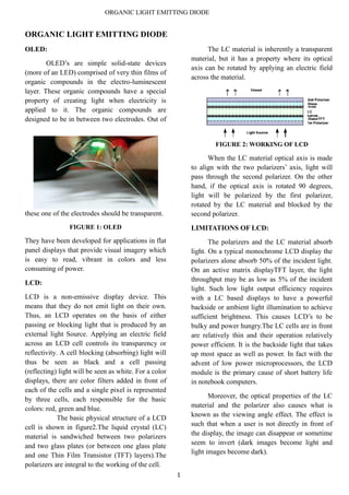
  • 1. ORGANIC LIGHT EMITTING DIODE ORGANIC LIGHT EMITTING DIODE OLED: The LC material is inherently a transparent material, but it has a property where its optical OLED’s are simple solid-state devices axis can be rotated by applying an electric field (more of an LED) comprised of very thin films of across the material. organic compounds in the electro-luminescent layer. These organic compounds have a special property of creating light when electricity is applied to it. The organic compounds are designed to be in between two electrodes. Out of FIGURE 2: WORKING OF LCD When the LC material optical axis is made to align with the two polarizers’ axis, light will pass through the second polarizer. On the other hand, if the optical axis is rotated 90 degrees, light will be polarized by the first polarizer, rotated by the LC material and blocked by the these one of the electrodes should be transparent. second polarizer. FIGURE 1: OLED LIMITATIONS OF LCD: They have been developed for applications in flat The polarizers and the LC material absorb panel displays that provide visual imagery which light. On a typical monochrome LCD display the is easy to read, vibrant in colors and less polarizers alone absorb 50% of the incident light. consuming of power. On an active matrix displayTFT layer, the light throughput may be as low as 5% of the incident LCD: light. Such low light output efficiency requires LCD is a non-emissive display device. This with a LC based displays to have a powerful means that they do not emit light on their own. backside or ambient light illumination to achieve Thus, an LCD operates on the basis of either sufficient brightness. This causes LCD’s to be passing or blocking light that is produced by an bulky and power hungry.The LC cells are in front external light Source. Applying an electric field are relatively thin and their operation relatively across an LCD cell controls its transparency or power efficient. It is the backside light that takes reflectivity. A cell blocking (absorbing) light will up most space as well as power. In fact with the thus be seen as black and a cell passing advent of low power microprocessors, the LCD (reflecting) light will be seen as white. For a color module is the primary cause of short battery life displays, there are color filters added in front of in notebook computers. each of the cells and a single pixel is represented by three cells, each responsible for the basic Moreover, the optical properties of the LC colors: red, green and blue. material and the polarizer also causes what is The basic physical structure of a LCD known as the viewing angle effect. The effect is cell is shown in figure2.The liquid crystal (LC) such that when a user is not directly in front of material is sandwiched between two polarizers the display, the image can disappear or sometime and two glass plates (or between one glass plate seem to invert (dark images become light and light images become dark). and one Thin Film Transistor (TFT) layers).The polarizers are integral to the working of the cell. 1
  • 2. ORGANIC LIGHT EMITTING DIODE EVOLUTION OF OLED: For an Organic LED, organic layer corresponding to the p-type material is called the The discovery of the electroluminescence hole-transport layer (HTL) and similarly the layer property in organic materials in 1950s is corresponding to the n-type material is called the considered to be the stepping stone of OLED. electron-transport layer (ETL). In Figure 3, Alq3 is the ETL and TPD is the HTL. Later in 1960, a scientist called Martin Pope discovered an ohmic, dark injecting Similar to doped silicon, when ETL and electrode contact to organic nature of crystals. HTL materials are placed to create a junction, the With this he was also able to explain the work energy bands equilibrates to maintain continuity functions for both the holes and electrons while across the structure. When a potential difference injecting electrode contacts. These dark injecting is applied across the structure, a drift current holes and electrons formed to be the base for an flows through the structure. The injected carries OLED device. The technique was further recombination at the junction consists of both experimented with DC electroluminescence under thermal and optical recombination, which emits different conditions. Later it was found that photons. electroluminescent materials can also act as doped insulators. Thus came the discovery of a double injection induced OLED device. The first proper OLED was manufactured in 1980 by Dr.Ching W Tang and Steven Van Slyke. The OLED had a double layer structure. When the holes and electrons were transported separately and when combined together produced a light in FIGURE 4: the organic layer centre. This light was produced OPTICAL RECOMBINATION IN OLED at a very low operating voltage with high Figure 4 shows optical recombination from the efficiency. energy band perspective. Note that LUMO is a Now more research is being done with the short form for Lowest Unoccupied Molecular application of OLED on polymer so as to obtain a Orbital, which corresponds to the conduction higher efficiency OLED. band in the energy diagram of doped silicon, and ORGANIC LED STRUCTURE: HOMO is a short form for Highest Occupied The p-n junction of oled is made from an organic Molecular Orbital, which corresponds to the compound such as: Alq3 (Aluminum tris (8- valence band in the energy diagram of doped hydroxyquinoline)) and diamine (TPD). The silicon. molecular structure of some typical organic Since an OLED emits light through a materials used are shown. recombination process, it does not suffer from the viewing angle limitation like an LC based device. Note that for any device to become a viable candidate for use in flat panel displays it has to be able to demonstrate high brightness, good power efficiency, good color saturation and sufficient lifetime. Reasonable lower limits specifications for any candidate device should include the following: brightness of ~ 100cd/m 2operating FIGURE 3: MOLECULAR STRUCTURE OF voltage of 5-15V. ORGANIC MATERIALS 2
  • 3. ORGANIC LIGHT EMITTING DIODE COMPONENTS IN AN OLED: The substrate is used to support the OLED. The anode is used to inject more holes The components in an OLED differ according to when there is a path of current. The conducting the number of layers of the organic material. layer is used to carry the holes from the anode. There is a basic single layer OLED, two layer and also three layer OLED’s. As the number of layers The cathode is used to produce electrons when increase the efficiency of the device also current flows through its path. The emissive layer increases. The increase in layers also helps in is the section where the light is produced. This injecting charges at the electrodes and thus helps layer is used to carry the electrons form the in blocking a charge from being dumped after cathode. reaching the opposite electrode. Any type of OLED consists of the following WORKING OF OLED: components.Emissive layer, Conducting layer, Before going on to the detailed Substrate, Anode and Cathode terminals. explanation of its working, it is important to know how the emissive layers and conducting layers are added to the substrate. There are mainly three basic methods for this operation. They are:- Inkjet Printing Technique – This is the cheapest and most commonly used technique. The method is same as the paper printing mechanism where the organic layers are sprayed onto the substrates. FIGURE 5: COMPONENTS OF OLED This method is also highly efficient and they can As the emissive layer and the conducting layer is be used for printing very large displays like made up of organic molecules (both being billboards and also big TV screens. different), OLED is considered to be an organic semi-conductor, and hence its name. The organic Organic Vapour Phase Deposition (OVPD) – This molecules have the property of conducting is also an efficient technique which can be carried electricity and their conducting levels can be out at a low cost. A cooled substrate is being hit varied form that of an insulator to a conductor. by the organic molecules, which was evaporated in a low pressure, high temperature chamber. The The emissive layer used in an OLED is made up of organic plastic molecules, out of which the gas is carried onto the substrate with the help of a most commonly used is polyfluorene. The carrier gas. conducting layer is also an organic molecule, and the commonly used component is polyaniline.The Vacuum Thermal Evaporation (VTE)-This substrate most commonly used may be a plastic, method is also commonly known as vacuum foil or even glass.The anode component should deposition method. This operation is carried out be transparent. Usually indium tin oxide is used. by gently heating the organic molecules so that This material is transparent to visible light. It also they evaporate and subside on the substrates. As has a great work function which helps in injecting the heating method is complicated and the holes into the different layers. The cathode strictness of parameters should be highly component depends on the type of OLED accurate, this method is economical as well. required. Even a transparent cathode can be used. After the organic material has been applied to the Usually metals like calcium and aluminium used substrate the real working of the OLED begins. because they have lesser work functions than OLEDs emit light in a similar manner to LEDs, anodes which helps in injecting electrons into the through a process called electrophosphorescence different layers. 3
  • 4. ORGANIC LIGHT EMITTING DIODE The battery or power supply of the device containing the OLED applies a voltage across the OLED. 1. Cathode (−), 2. Emissive Layer, 3. Emission FIGURE 7: VARIATION OF I-V of radiation, 4. Conductive Layer, 5. Anode (+) CHARACTERISTIC WITH TEMPERATURE FIGURE 6: WORKING OF OLED Besides temperature, the I-V characteristic Electrical current flows from the cathode also depends strongly on the type of to the anode through the organic layers (an anode/cathode used in the device as well as the electrical current is a flow of electrons). The thickness of the organic active Electro cathode gives electrons to the emissive layer of Luminescence (EL) layer. The particular Figure organic molecules.The anode removes electrons shows the I-V characteristic variation with the from the conductive layer of organic molecules. thickness of the organic layer. (This is the equivalent to giving electron holes to the conductive layer). At the boundary between the emissive and the conductive layers, electrons find electron holes. When an electron finds an electron hole, the electron fills the hole (it falls into an energy level of the atom that is missing an electron). When this happens, the electron gives up energy in the form of a photon of light. The OLED emits light. FIGURE 8: VARIATION OF I-V The color of the light depends on the type CHARACTERISTIC WITH THICKNESS of organic molecule in the emissive layer. Manufacturers place several types of organic MODERN TECHNOLOGIES IN OLED’S films on the same OLED to make color displays. (1)High Efficiency Materials: The intensity or brightness of the light depends These materials emit light through on the amount of electrical current applied. The the process of electrophosphorescence. In more the current, the brighter the light. traditional OLEDs, the light emission is based I-V CHARACTERISTIC VARIATION: on fluorescence, a transition from a singlet The I-V characteristics of OLED is also excited state of a material. According to varying with time. Several factors contribute to theoretical and experimental estimation, the the I-V characteristic variation. The first and upper limit of efficiency of an OLED doped foremost is temperature. The I-V characteristic with fluorescent material, is approximately depends quite strongly on the operating 25%. temperature. The I-V characteristic variation pose With our electro phosphorescent a challenge to the control of OLED based materials used as a dopant, which exploits both displays as the I-V operating points have to be singlet and triplet excited states, this upper shifted depending on the operating temperature as limit is virtually eliminated. We are equipped shown in figure 7. with the potential of 100% efficiency. 4
  • 5. ORGANIC LIGHT EMITTING DIODE We are working towards the In an active matrix OLED display commercialization of electro phosphorescent (AMOLED), information is sent to the transistor devices by optimizing the device efficiency, in each pixel, telling it how bright the pixel color purity and device storage and operation should shine. The TFT then stores this durabilities. information and continuously controls the current flowing through the OLED. In this way the OLED is operating all the time, avoiding the need for the very high currents necessary in a passive matrix display. The new high efficiency material systems are ideally suited for use in active matrix OLED displays, and their high efficiencies should result in greatly reduced power consumption. This type of OLED is suitable for high resolution and large size display. Though the manufacturing process is the same, the anode FIGURE 9: TRIPLET EMITTER layers have a Thin-film transistor (TFT) plane in Such a process is facilitated by the parallel to it so as to form a matrix. This helps in development and modification of charge switching each pixel to it’s on or off state as transport materials, charge blocking materials desired, thus forming an image. This is the least and luminescent materials, and their power consuming type among others and also has incorporation into devices. In addition to the quicker refresh rates which makes them suitable fabrication of high quality devices, UDC is also for video as well. committed to a high standard of device testing. (3)Passive Matrix OLED (PMOLED): Our scientists and engineers have custom developed sophisticated test hardware and Passive Matrix displays consist of an software for this purpose. array of picture elements, or pixels, deposited on (2)Active Matrix OLED (AMOLED): a patterned substrate in a matrix of rows and columns. In an active matrix display, the array is still divided into a series of row and column lines, with each pixel formed at the intersection of a row and column line. However, each pixel now consists of an organic light emitting diode (OLED) in series with a thin film transistor (TFT). The TFT is a switch that can control the amount of current flowing through the OLED. FIGURE 11: PMOLED In an OLED display, each pixel is an organic light emitting diode, formed at the intersection of each column and row line. The first OLED displays, like the first LCD, are addressed as a passive matrix. This means that to illuminate any particular pixel, electrical signals FIGURE 10: AMOLED are applied to the row line and column line (the intersection of which defines the pixel). 5
  • 6. ORGANIC LIGHT EMITTING DIODE The more current pumped through each FOLEDs are organic light emitting devices pixel diode, the brighter the pixel looks to our built on flexible substrates. Flat panel displays eyes.The design of this type of OLED makes have traditionally been fabricated on glass them more suitable for small screen devices like substrates because of structural and/or processing cell phones, MP3 players and so on. Though this constraints. Flexible materials have significant type is less power consuming than an LCD and performance advantages over traditional glass LED (even if connected to other external substrates. circuitry’s), it is the most power consuming FOLEDs Offer Revolutionary Features for comparative to other OLED’s. Displays: This type is very easy to make as strips of (i)Flexibility: For the first time, FOLEDs may anode and cathode are kept perpendicular to each be made on a wide variety of substrates that other. When they are both intersected light is range from optically-clear plastic films to produced. As there are strips of anode and reflective metal foils. These materials provide cathode, current is applied to the selected strips the ability to conform, bend or roll a display and is applied to them. This helps in determining into any shape. This means that a FOLED the on or off pixels. display may be laminated onto a helmet face shield, a military uniform shirtsleeve, an (4)Inverted OLED: aircraft cockpit instrument panel or an automotive windshield. (ii)Ultra-lightweight, thin form: The use of thin plastic substrates will also significantly reduce the weight of flat panel displays in cell phones, portable computers and, especially, large-area televisions-on-the-wall. For example, the weight of a display in a laptop may be significantly reduced by using FOLED FIGURE 12: INVERTED OLED technology. This type uses a bottom cathode, which is (iii)Durability: FOLEDs will also generally be connected to the drain end of an n-channel TFT less breakable, more impact resistant and more backplane. This method is usually used for durable compared to their glass-based producing low cost OLED with little applications. counterpart. (5)Foldable OLED (FOLED): (iv)Cost-effective processing: OLEDs are projected to have full-production level cost advantage over most flat panel displays. With the advent of FOLED technology, the prospect of roll-to-roll processing is created. To this end, our research partners have demonstrated a continuous organic vapor phase deposition (OVPD) process for large-area roll-to-roll OLED processing. While continuous web FOLED processing requires further development, this process may provide the FIGURE 13: FOLDABLE OLED basis for very low-cost, mass production. 6
  • 7. ORGANIC LIGHT EMITTING DIODE This type is mainly used in devices which have more chance of breaking. As this material is strong it reduces breakage and therefore is used in cell phones, computer chips, GPS devices and PDA’s. They are also flexible, durable and lightweight. As its name explains, these OLED’s are foldable and can also be connected to clothes. They use different types of substrates like flexible metallic foils, plastics and so on. (6)Top Emitting OLED: This type of OLED is integrated with a transistor backplane that is not transparent. Such devices are suitable for matrix applications like FIGURE 15: TRANSPARENT OLED smart cards. The substrate used for this device is This device has a good contrast even in of the opaque/reflective type. As a transparent bright sunlight so it is applicable in head-up substrate is used the electrode used is either semi- displays, mobile phones, smart windows and so transparent or fully transparent. Otherwise the on. In this device, the entire anode, cathode and light will not pass through the transparent the substrate are transparent. When they are in the substrate. off position, they become almost completely transparent as their substrate. This type of OLED can be included in both the active and passive matrix categories. As they have transparent parameters on both the sides, they can create displays that are top as well as bottom emitting. (8)White OLED: White OLEDs emit white light that is brighter, more uniform and more energy efficient than that emitted by fluorescent lights. White FIGURE 14: TOP EMITTING OLED OLEDs also have the true-color qualities (7)Transparent OLED: of incandescent lighting. Because OLEDs can be made in large sheets, they can replace fluorescent The Transparent OLED (TOLED) uses a lights that are currently used in homes and proprietary transparent contact to create displays buildings. Their use could potentially reduce that can be made to be top-only emitting, bottom- energy costs for lighting. only emitting, or both top and bottom emitting (transparent). TOLEDs can greatly improve contrast, making it much easier to view displays in bright sunlight. Because TOLEDs are 70% transparent when turned off, they may be integrated into car windshields, architectural windows, and eyewear. Their transparency enables TOLEDs to be used with metal, foils, silicon wafers and other opaque substrates for FIGURE 16: WHITE OLED top-emitting devices. 7
  • 8. ORGANIC LIGHT EMITTING DIODE This device creates the brightest light of all. This device uses the composite colours as They are manufactured in large sheets. Thus they sub pixels and also on top of each other. This can easily replace fluorescent lamps. They are causes the reduction in pixel gap and also an also cost-effective and also consumes less power. increase in colour depth. Thus they are being (9)Stacked OLED (SOLED): introduced as television displays. The Stacked OLED (SOLED) uses (10)ORGANIC LASERS: Universal Display Corporation's award- An organic laser is a solid-state winning, novel pixel architecture that is based device based on organic materials and on stacking the red, green, and blue subpixels structures similar to those used in UDC's on top of one another instead of next to one display technologies. An optically-pumped another as is commonly done in CRTs and organic laser demonstrates five key laser LCDs. This improves display resolution up to characteristics: spatial coherence, a clear three-fold and enhances full-color quality. threshold, strongly polarized light emission, SOLEDs may provide the high resolution spectral line narrowing, and the existence of needed for wireless worldwide-web laser cavity modes. To realize commercial applications. potential, the key technical challenge today is to demonstrate a mechanism for the electrical pumping of these lasers. The use of small-molecule organic materials opens the door to an entirely new class of light emitters for diode lasers. These organic lasers may offer: a) Greater color variety b) Tunability c) Further miniaturization FIGURE 17: STACKED OLED d) Easier processing SOLED DISPLAY: e) Lower cost in a host of end uses A SOLED display consists of an ORGANIC VAPOUR PHASE DEPOSITION: array of vertically-stacked TOLED sub-pixels. To separately tune color and brightness, each The OVPD production process of the red, green and blue (R-G-B) sub-pixel utilizes a carrier gas stream in a hot walled elements is individually controlled. By reactor at very low pressure to precisely deposit adjusting the ratio of currents in the three the thin layers of organic materials used in elements, color is tuned. By varying the total OLED displays. Conventional OLED current through the stack, brightness is varied. fabrication equipment evaporates the organic By modulating the pulse width, gray scale is molecules at high temperature and pressure. achieved. With this SOLED architecture, each OVPD offers the ability to precisely control the pixel can, in principle, provide full color. multi-source deposition required for full-color Universal Display Corporation's SOLED OLED displays. The OVPD design should also technology may be the first demonstration of be adaptable to the rapid, uniform deposition of an vertically-integrated structure where organics on large-area substrates and for roll- intensity, color and gray scale can be to-roll processing. The technology, Organic independently tuned to achieve high-resolution Vapour Phase Deposition can enable low cost, full-color. precise, high throughput process for fabricating OLEDs. 8
  • 9. ORGANIC LIGHT EMITTING DIODE ADVANTAGES OF OLED: 7.Efficient in Energy: OLED displays consumes less energy as compared to LCD displays and The different manufacturing process of other display screens. No backlight is required in OLEDs lends itself to several advantages over these screens which is the biggest OLED flat-panel displays made with LCD technology. advantage for use in portable gadgets. 1. Lower cost in the future: OLEDs can be 8.Good for Eyes: Another great advantage of printed onto any suitable substrate by an inkjet OLED is that it pts less stains on eyes and hence printer or even by screen printing,[52] theoretically are eye soothening. These screens provide better making them cheaper to produce than LCD or viewing experience because they have better plasma displays. However, fabrication of the contrast, brightness and color aspects. OLED substrate is more costly than that of a TFT LCD, until mass production methods lower cost 9.Self luminous: The OLED is self luminous i.e. through scalability. it creates the required light energy on its own. It does not require any external source for creating 2. Light weight & flexible plastic substrates: light like LCD. OLED displays can be fabricated on flexible plastic substrates leading to the possibility of 10.Environmental drawbacks: There are no Organic light-emitting diode roll-up display being environmental drawbacks while using OLED as it fabricated or other new applications such as roll- uses organic materials. up displays embedded in fabrics or clothing. As the substrate used can be flexible such as PET, 11.Power in-take: OLED does not require any the displays may be produced inexpensively. power in take when turned off. 3. Wider viewing angles & improved 12.Durability: Another great advantage of OLED brightness: OLEDs can enable a greater artificial is that it is more durable than traditional screens. contrast ratio (both dynamic range and static, There chance of getting broken is comparitively measured in purely dark conditions) and viewing less to LCD screens and other displays. angle compared to LCDs because OLED pixels directly emit light. OLED pixel colours appear DISADVANTAGES OF OLED: correct and unshifted, even as the viewing angle approaches 90 degrees from normal. 1.Lifespan: The biggest technical problem for OLEDs was the limited lifetime of the organic 4. Better power efficiency: LCDs filter the light materials. In particular, blue OLEDs historically emitted from a backlight, allowing a small have had a lifetime of around 14,000 hours to half fraction of light through so they cannot show true original brightness (five years at 8 hours a day) black, while an inactive OLED element does not when used for flat-panel displays. This is lower produce light or consume power. than the typical lifetime of LCD, LED or PDP technology—each currently rated for about 5. Response time: OLEDs can also have a faster 25,000 - 40,000 hours to half brightness, response time than standard LCD screens. depending on manufacturer and model. Whereas LCD displays are capable of a 1 ms response time or less offering a frame rate of 2.Color balance issues: Additionally, as the 1,000 Hz or higher, an OLED can theoretically OLED material used to produce blue light degrades significantly more rapidly than the have less than 0.01 ms response time enabling materials that produce other colors, blue light 100,000 Hz refresh rates. output will decrease relative to the other colors of light. This differential color output change will 6.Slimmer: The biggest adavantage of OLED change the color balance of the display and is screen is that it is slimmer than LCD display. much more noticeable than a decrease in overall While LCD and Plasma displays could be few luminance. This can be partially avoided by inches thick, OLED advantage is that it is only adjusting colour balance but this may require few millimeters thick. advanced control circuits. 9
  • 10. ORGANIC LIGHT EMITTING DIODE 3.Efficiency of blue OLEDs: Improvements to the efficiency and lifetime of blue OLEDs is vital to the success of OLEDs as replacements for LCD technology. Considerable research has been invested in developing blue OLEDs with high external quantum efficiency as well as a deeper blue color. 4.Water damage: Water can damage the organic materials of the displays. Therefore, improved sealing processes are important for practical FIGURE 18: MOBILE WITH OLED manufacturing. Water damage may especially DISPLAY limit the longevity of more flexible displays. 16) Smart goggles/helmets for scuba divers, 5.UV sensitivity: OLED displays can be motorcycle riders damaged by prolonged exposure to UV light. 17) Medical test equipment PRODUCT CONCEPTS 18) Wide area, full-motion video camcorders Universal Display Corporation has only 19) Global positioning systems (GPS) begun to imagine what our OLED technology 20) Integrated computer displaying eyewear can create in the way of products for our world 21) Rugged military portable communication and our future. The technology has the potential devices to not only improve existing products, but also ORGANIC FUTURE to create exciting, new product possibilities, for The first products using organic displays example: are already being introduced into the market 1) Low-power, bright, colorful cell phones place. And while it is always difficult to predict 2) Full color, high-resolution, personal when and what future products will be communicators introduced, many manufacturers are now 3) Wrist-mounted, featherweight, rugged PDAs working to introduce cell phones and personal 4) Wearable, form-fitting, electronic displays digital assistants with OLED displays within the 5) Full-color, high resolution, portable Internet next one or two years. The ultimate goal of devices and palm size computers using high-efficiency, phosphorescence, flexible 6) High-contrast automotive instrument and OLED displays in lap top computers and even windshield displays for home video applications may be no more 7) Heads-up instrumentation for aircraft and than a few years into future. automobiles 8) Automobile light systems without bulbs 9) Flexible, lightweight, thin, durable, and highly efficient laptop screens 10) Roll-up, electronic, daily-refreshable newspaper 11) Ultra-lightweight, wall-size television monitor 12) Office windows, walls and partitions that FIGURE 19: IDENTITY CARD WITH OLED double as computer screens DISPLAY 13) Color-changing lighting panels and light However, there remains much to be done walls for home and office if organics are to establish a foothold in the 14) Low-cost organic lasers display market. Achieving higher efficiencies, 15) Computer-controlled, electronic shelf pricing lower operating voltages, and lower device life for supermarkets and retail stores times are all challenges still to be met. 10
  • 11. ORGANIC LIGHT EMITTING DIODE Given the aggressive worldwide efforts REFERENCES: in this area, emissive organic thin films have an 1. "Brief OLED history". Comboled Project excellent chance of becoming the technology of 2. "Organic electroluminescent diodes". choice for the next generation of high- Applied Physics Letters resolution, high-efficiency flat panel displays. 3. Electronic processes in organic crystals and polymers, 2nd ed., by M. Pope 4. Wikipedia.com FIGURE 20: OLED DISPLAY In addition to displays, there are many other opportunities for application of organic thin-film semiconductors, but to date these have remained largely untapped. Recent results in organic electronic technology that may soon find commercial outlets in display black planes and other low-cost electronics. FIGURE 21: WATCH WITH OLED DISPLAY CONCLUSION: OLEDs offer many advantages over both LEDs and LCDs. They are thinner, lighter and more flexible than the crystalline layers in an LED or LCD. They have large fields of view as they produce their own light. Research and development in the field of OLEDs is proceeding rapidly and may lead to future applications in heads up displays, automotive dash boards, billboard type displays etc. Because OLEDs refresh faster than LCDs, a device with OLED display could change information almost in real time. Video images could be much more realistic and constantly updated. 11