1. 技術情報 Technical Information
di/dt測定/di/dt Test
PN接合ダイオードまたは金属とN形半導体を接触させたショットキ configuration of the power MOS-FET.
ーバリアダイオード等は、整流作用を持っている。
2極の接合面であるアノードとカソード間には空乏層による接合容 +VS
量があり、ダイオードの理想的動きを阻害している。 Q1 Q3
ダイオードに順方向電流IFが流れている時、このダイオードに逆方 ①id1
向電圧(VR)を印加すると、理想的にはfig-1の様にIF電流が停止する M
だけであるが、実際はfig-2の様にPN接合の近傍に小数キャリアが残 AC
②idf2
IN
っている間、逆方向であるにも関わらず大きな逆電流(IR)が流れる。 ③idr
Q2 Q4
電流の零クロス点からI r p の1 0 % に戻るまでの時間を逆回復時間
(trr=Reverse Recovery Time)と言い、ダイオードのスイッチング特
fig-3
性として小さいことが望まれる。また、Trrが大きい場合は使用条件
次第では破壊の要因ともなる。 上下交互にON/OFFを繰り返し、そのON/OFF時間を変化させる
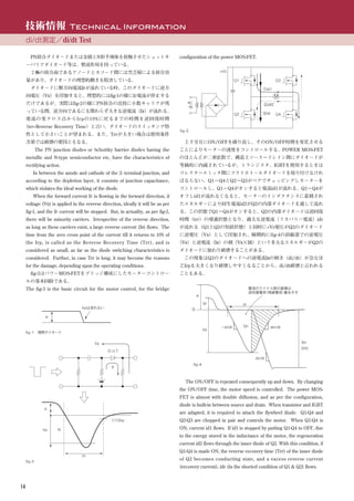
The PN junction diodes or Schottky barrier diodes having the ことによりモーターの速度をコントロールする。POWER MOS-FET
metallic and N-type semiconductor etc, have the characteristics of のほとんどが二重拡散で、構造上ソース−ドレイン間にダイオードが
rectifying action. 等価的に内蔵されているが、トランジスタ、IGBTを使用するときは
In between the anode and cathode of the 2- terminal junction, and コレクタ−エミッタ間にフライホイールダイオードを取り付けなけれ
according to the depletion layer, it consists of junction capacitance, ばならない。Q1−Q4とQ2−Q3がペアでチョッピングしモーターを
which violates the ideal working of the diode. コントロールし、Q1−Q4がオンすると電流id1が流れる。Q1−Q4が
When the forward current IF is flowing in the forward direction, if オフしid1が流れなくなると、モーターのインダクタンスに蓄積され
voltage (VR) is applied in the reverse direction, ideally it will be as per たエネルギーにより回生電流id2がQ2の内部ダイオードを通して流れ
fig-1, and the IF current will be stopped. But, in actuality, as per fig-2, る。この状態でQ1−Q4がオンすると、Q2の内部ダイオードは逆回復
there will be minority carriers. Irrespective of the reverse direction, 時間(trr)の導通状態となり、過大な逆電流(リカバリー電流)idr
as long as these carriers exist, a large reverse current (IR) flows. The が流れる(Q1とQ2の短絡状態)と同時に+VS電圧がQ2のダイオード
time from the zero cross point of the current till it returns to 10% of に逆電圧(V R)として印加され、瞬間的にfig-4の斜線部での逆電圧
the Irp, is called as the Reverse Recovery Time (Trr), and is (VR)と逆電流(IR)の積(VR×IR)という多大なエネルギーがQ2の
considered as small, as far as the diode switching characteristics is ダイオードに加わり破壊することがある。
considered. Further, in case Trr is long, it may become the reasons この現象はQ2のダイオードへの逆電流IRの傾き(di/dt)が急なほ
for the damage, depending upon the operating conditions. どIrpも大きくなり破壊しやすくなることから、di/dt破壊と言われる
fig-3はパワーMOS-FETをブリッジ構成にしたモーターコントロー こともある。
ルの基本回路である。
The fig-3 is the basic circuit for the motor control, for the bridge 電流のマイナス部の面積は
逆回復電荷
(残留電荷)量を示す
IF
VF trr
Irpは流れない 0
IF
−di/dt Qrr dirr/dt
Irp
fig-1 理想ダイオード
Irp Vrr
(VR)
D.U.T
dv/dt
fig-4
IF
The ON/OFF is repeated consequently up and down. By changing
the ON/OFF time, the motor speed is controlled. The power MOS-
FET is almost with double diffusion, and as per the configuration,
diode is built-in between source and drain. When transistor and IGBT
IF
are adapted, it is required to attach the flywheel diode. Q1-Q4 and
1/10Irp Q2-Q3 are chopped in pair and controls the motor. When Q1-Q4 is
Irp IR ON, current id1 flows. If id1 is stopped by putting Q1-Q4 to OFF, due
to the energy stored in the inductance of the motor, the regeneration
current id2 flows through the inner diode of Q2. With this condition, if
Q1-Q4 is made ON, the reverse recovery time (Trr) of the inner diode
trr
fig-2
of Q2 becomes conducting state, and a excess reverse current
(recovery current), idr (in the shorted condition of Q1 & Q2) flows.
14
2. 技術情報 Technical Information
di/dt測定/di/dt Test
D.U.T.
VDS L
SHORT IDR
ID電流検出 IL + Vrr
BNC-R 電源
−
RG ドライバー
PULSE FET
GENE
fig-5 di/dt破壊波形 fig-6 基本測定回路
At the same time, the +VS (supply voltage) is applied to the diode of di/dt試験の必要性
Q2, as the reverse voltage (VR). Instantaneously as per fig-4, in the The need of the di/dt test
shaded area, it results in high energy, V R×I R, with the reverse
current (IR) and reverse voltage (VR). This energy is applied to the ダイオードは電流に強く、短時間なら少々の無理をしても壊れるこ
diode of Q2, resulting in the damage. とはない、と思うのが多くの技術者の感覚だろう。しかし、この
This phenomenon becomes severe, when di/dt of the reverse di/dt破壊については知っておく必要がある。なぜなら、di/dt破壊は
current I R of the diode of Q2 is quick, which makes Irp larger, 高温(80℃以上)になると発生しやすく、di/dt耐量はカタログ上の
resulting in the damage. This may also be called as the di/dt damage. 静特性データからは読み取ることはできないからだ。MOS-FET使用
の機器で設計上は問題がないにもかかわらず、使用中にMOS-FETの
di/dt測定おけるdi/dtの傾き 破壊が発生する場合などはdi/dt破壊を考える必要がある。
Tilt of di/dt in the measurement of di/dt 製品が小型化し、様々な環境のもとで使用される半導体にとって、
di/dt試験は重要な項目といえる。
di/dt測定の基本測定回路をfig-6に示す。di/dtの傾きは、ドライバ Most engineers might think that diodes are resistant to current
ーFET、被測定素子、回路インダクタンス等により大きく値が変わる。 and will not be broken by a little overwork for a short time. However,
また、テスターのヘッドボックス測定においても、テストソケットや it is necessary to know about this di/dt damage. It is because di/dt
テスター内部配線等により約150nH前後の浮遊インダクタンスができ damage is likely to occur in high-temperature environment, and di/dt
てしまう。 strength is unable to be grasped from static characteristic data shown
測子ケーブル10cmを100nHとし、回路インダクタンスのみで、ほ on catalogs. If damage of MOS-FET occurs even if there is no design
かのドライバーFET等は最良として計算するとfig-7のようになる。 defect in apparatuses using MOS-FETs, di/dt damage should be
The fundamental measurement circuit for the di/dt measurement considered as a cause.
is as per fig-6. The tilt in di/dt is greatly changed according to the Miniaturization of products has been improved. The di/dt test is a
driver FET, DUT, circuit inductance etc. Further, for the significant item for semiconductors used in various environments.
measurement using tester head box, it may create a residual
inductance of the order of 150nH due to the internal wiring of the
tester and test socket.
If the measurement cable of 10cm is considered as 100nH, fig-7
indicates the calculation for the driver FET, based only on the circuit
inductance.
測定環境
ヘッドボックス ヘッドボックス ヘッドボックス
(150nH) +測子ケーブル +測子ケーブル
Vrr 10cm 20cm
(250nH) (350nH)
Vrr=100V 660A/μS 400A/μS 280A/μS
Vrr=200V 1300A/μS 800A/μS 570A/μS
Vrr=300V 2000A/μS 1200A/μS 850A/μS
fig-7 測子ケーブル長と最大di/dtの目安
15