1. GaSb/GaAs Quantum Dot Solar CellsGaSb/GaAs Quantum Dot Solar Cells
Richard A. Gaona, Ramesh B. Laghumavarapu, Diana L. HuffakerRichard A. Gaona, Ramesh B. Laghumavarapu, Diana L. Huffaker
Abstract: Recently self-assembled quantum dots (QD) have been explored for high efficiencies in solar cells. In this work, we present the study of GaSb QDs in a GaAs matrix. 5 layers of GaSb QDs are inserted into
the intrinsic region of a GaAs p-i-n solar cell. These solar cells are characterized for optical and electrical properties via photoluminescence, I-V and spectral response measurements. The performance of GaSb QD solar cells has also
been compared with a GaAs control cell (with no QDs). The short circuit current, open circuit voltage and fill factors in the QDSC and control cells are 2.09788 mA, 0.600045 V, 65.07064 and 2.36410 mA, 0.920038 V, 76.92086
respectively. The GaSb QD solar cells have shown an extended spectral response (up to 1250 nm) compared GaAs control cell (900 nm) indicating QD contribution to photocurrent.
Motivation: In single junction cells the maximum energy conversion efficiency is limited to 33%. Quantum dot solar cells (QDSC) have potential for high efficiency (63%) with less complexity and cost. Moreover,
quantum confinement can be realized in order to expand spectral response. With proper choice of QD and barrier materials, QDSCs can be exploited to utilize carrier multiplication. GaSb QDs in GaAs matrix have longer carrier lifetimes
and longer wavelength absorption compared to well established InAs QDs. These qualities make GaSb/GaAs system attractive for high efficiency solar cells.
Background
Quantum Dots
Quantum confinement occurs as we define a family of
valid wave functions for carriers. To do so, we let the
dimensions of our quantum dots approach the carrier’s
deBroglie wavelength. As the energy of states varies with
volume, we can tune the band gap of our QDs. Thus, we
can insert these dots into the intrinsic region of a p-i-n
junction to absorb photons of energy less than that of the
junction band gap.1, 3, 4
Growth
We use molecular beam epitaxy in Stranski-Krastanov
mode to grow our GaSb/GaAs quantum dot solar cells.
Lattice mismatch (~7.8%) between GaSb & GaAs leads
to self-organized growth of islands, our quantum dots.
Five layers of dots are grown in the intrinsic region of
the p-i-n junction. Currently, no strain compensation is
employed in these devices.1, 3
GaSb/GaAs QDSCs
GaSb1
•Type II band structure
•Spatially indirect excitons
•Hole confinement of 540 meV
•Longer carrier lifetimes
•Increased infrared absorption up to 1250 nm
•Difficulty due to strong As/Sb intermixing
•Accumulation of strain as layers increase
Device Description
•P-i-n junction w/5 stack of QDs in i-region
•Spacers inserted between dot stacks to reduce
coupling & alleviate strain
•Stacking to inc. absorption causes strain that
deteriorates device performance
•5x5, 3x3, 2x2 (mm2
) cells
•SK growth allows for high dot density & small size
(~10-9
m)
•Constraints: dot size, uniformity, density1, 3
I-V Characterization Future Work
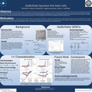
Test Parameters2
Short Circuit Current
Open Circuit Voltage
Fill Factor
Efficiency
ISC ≈ −IL (RP → ∞ ,VBias = 0)
Voc ≈
nkT
q
ln
ISC
I0
(I = 0,I0 = T
3
2
e
−Eg
nkT
)
FF =
Pmax
ISCVOC
Growth
•Strain compensation
•Different growing modes (IMF)
•Different materials (graphene?)5
•Passivation
•Better resolution
Device Design
•Anti-reflection coating
•Intermediate band
•Carrier multiplication
•Stack optimization
•QD coupling
Conclusions
Acknowledgements
Quantum dot solar cells posses certain theoretical
qualities that will increase the absorption
spectrum and efficiency of solar cells. Many
steps must be taken to ensure dot uniformity and
proper density and size during growth. Low FFs
show a great deal of defects in our GaSb/GaAs
quantum dot solar cells. Compared to control
cells, we have lower Isc & Voc, but a significant
improvement in absorption after 1100nm. Many
of these defects are caused by strain introduced
during quantum dot growth. Therefore, there is a
great deal of work to be done to reduce such
dislocations and move device performance to the
ideal case by optimizing manufacturing methods.
I would like to thank Diana Huffaker and her lab for all their hard work, Lockheed Martin for
their generous donation, and, most of all, Rick Ainsworth, Audrey Pool O’Neal, and the entire
CEED organization for allowing me this opportunity to broaden my education
References1.Laghumavrapu, Ramesh B., 2008, InAs/GaAs and GaSb/GaAs Quantum Dot Solar Cells, University of New Mexico, Albuquerque, 83 p.
2.Bowden, S., Honsberg, C., 2010, Solar Cell Operation, http://www.pveducation.org/pvcdrom/solar-cell-operation/solar-cell-structure (July 1, 2010)
3.Bimberg, D., et al.,1999, Quantum Dot Heterostructures, Wiley, West Sussex, 328 p.
4.Ryne P. Raffaelle, Stephanie L. Castro, Aloysius F. Hepp and Sheila G. Bailey, Prog. Photovolt: Res. Appl. 2002; 10:433–439
5.Berger, M., 2008, Graphene quantum dots as single-electron transistors, http://www.nanowerk.com/spotlight/spotid=5433.php (August 15, 2010)
6.Equivalent Circuit of a Solar Cell, Solar Cell, http://en.wikipedia.org/wiki/File:Solar_cell_equivalent_circuit.svg (August 15, 2010)
Photo courtesy of wikipedia.org6
I = ID + ISH − IL
AFM: GaSb/GaAs QD
P - Substrate
P - Base
N - Emitter
Quantum dots
15 nm
GaAs GaSb QD
Photos courtesy of Ramesh Laghumavarapu
Photo courtesy of Charles Reyner
Under Light Isc (mA) Voc (V) FF Efficiency
QDSC 2.09788 0.600045 65.07064 0.032765
Control Cell 2.36410 0.920038 76.92086 0.066923
η =
Pmax
Pin
=
VOC ISC FF
Pin
Type II Band Gap
CB
GaAs
GaSb
GaAs
VB
~500meV
Light and dark QDSC and Control Cell current-voltage plots, used to derive Voc,
Isc, FF, and efficiency. Light measurements were taken under AM 1.5 spectrum.
PL intensity showing QD contribution
to infrared absorption
Indirect excitons