Advanced HEXFET Power MOSFET
•
0 likes•1,143 views

The document summarizes the specifications and characteristics of the IRF3415 HEXFET Power MOSFET. It provides detailed technical specifications for the device, which utilizes advanced processing to achieve low resistance and fast switching for efficient and reliable operation. Key specifications include a continuous drain current of 43A, on-resistance of 0.042 ohms, and operating temperature range of -55°C to +175°C.

Recommended
Recommended
More Related Content
What's hot
What's hot (20)
Viewers also liked
Similar to Advanced HEXFET Power MOSFET
Similar to Advanced HEXFET Power MOSFET (20)
Recently uploaded
Recently uploaded (20)
Advanced HEXFET Power MOSFET
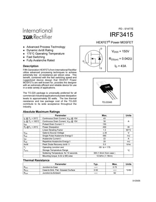
- 1. IRF3415 HEXFET® Power MOSFET Fifth Generation HEXFETs from International Rectifier utilize advanced processing techniques to achieve extremely low on-resistance per silicon area. This benefit, combined with the fast switching speed and ruggedized device design that HEXFET Power MOSFETs are well known for, provides the designer with an extremely efficient and reliable device for use in a wide variety of applications. The TO-220 package is universally preferred for all commercial-industrialapplicationsatpowerdissipation levels to approximately 50 watts. The low thermal resistance and low package cost of the TO-220 contribute to its wide acceptance throughout the industry. S D G Parameter Max. Units ID @ TC = 25°C Continuous Drain Current, VGS @ 10V 43 ID @ TC = 100°C Continuous Drain Current, VGS @ 10V 30 A IDM Pulsed Drain Current 150 PD @TC = 25°C Power Dissipation 200 W Linear Derating Factor 1.3 W/°C VGS Gate-to-Source Voltage ± 20 V EAS Single Pulse Avalanche Energy‚ 590 mJ IAR Avalanche Current 22 A EAR Repetitive Avalanche Energy 20 mJ dv/dt Peak Diode Recovery dv/dt ƒ 5.0 V/ns TJ Operating Junction and -55 to + 175 TSTG Storage Temperature Range Soldering Temperature, for 10 seconds 300 (1.6mm from case ) °C Mounting torque, 6-32 or M3 srew 10 lbf•in (1.1N•m) Absolute Maximum Ratings Parameter Typ. Max. Units RθJC Junction-to-Case ––– 0.75 RθCS Case-to-Sink, Flat, Greased Surface 0.50 ––– °C/W RθJA Junction-to-Ambient ––– 62 Thermal Resistance VDSS = 150V RDS(on) = 0.042Ω ID = 43A TO-220AB l Advanced Process Technology l Dynamic dv/dt Rating l 175°C Operating Temperature l Fast Switching l Fully Avalanche Rated Description 01/25/05 PD - 91477E
- 2. IRF3415 Parameter Min. Typ. Max. Units Conditions IS Continuous Source Current MOSFET symbol (Body Diode) ––– ––– showing the ISM Pulsed Source Current integral reverse (Body Diode) ––– ––– p-n junction diode. VSD Diode Forward Voltage ––– ––– 1.3 V TJ = 25°C, IS = 22A, VGS = 0V „ trr Reverse Recovery Time ––– 260 390 ns TJ = 25°C, IF = 22A Qrr Reverse RecoveryCharge ––– 2.2 3.3 µC di/dt = 100A/µs „ Source-Drain Ratings and Characteristics S D G Parameter Min. Typ. Max. Units Conditions V(BR)DSS Drain-to-Source Breakdown Voltage 150 ––– ––– V VGS = 0V, ID = 250µA ∆V(BR)DSS/∆TJ Breakdown Voltage Temp. Coefficient ––– 0.17 ––– V/°C Reference to 25°C, ID = 1mA RDS(on) Static Drain-to-Source On-Resistance ––– ––– 0.042 Ω VGS = 10V, ID = 22A „ VGS(th) Gate Threshold Voltage 2.0 ––– 4.0 V VDS = VGS, ID = 250µA gfs Forward Transconductance 19 ––– ––– S VDS = 50V, ID = 22A ––– ––– 25 µA VDS = 150V, VGS = 0V ––– ––– 250 VDS = 120V, VGS = 0V, TJ = 150°C Gate-to-Source Forward Leakage ––– ––– 100 VGS = 20V Gate-to-Source Reverse Leakage ––– ––– -100 nA VGS = -20V Qg Total Gate Charge ––– ––– 200 ID = 22A Qgs Gate-to-Source Charge ––– ––– 17 nC VDS = 120V Qgd Gate-to-Drain ("Miller") Charge ––– ––– 98 VGS = 10V, See Fig. 6 and 13 „ td(on) Turn-On Delay Time ––– 12 ––– VDD = 75V tr Rise Time ––– 55 ––– ID = 22A td(off) Turn-Off Delay Time ––– 71 ––– RG = 2.5Ω tf Fall Time ––– 69 ––– RD = 3.3Ω, See Fig. 10 „ Between lead, ––– ––– 6mm (0.25in.) from package and center of die contact Ciss Input Capacitance ––– 2400 ––– VGS = 0V Coss Output Capacitance ––– 640 ––– pF VDS = 25V Crss Reverse Transfer Capacitance ––– 340 ––– ƒ = 1.0MHz, See Fig. 5 nH Electrical Characteristics @ TJ = 25°C (unless otherwise specified) LD Internal Drain Inductance LS Internal Source Inductance ––– ––– S D G IGSS ns 4.5 7.5 IDSS Drain-to-Source Leakage Current Repetitive rating; pulse width limited by max. junction temperature. ( See fig. 11 ) ƒ ISD ≤ 22A, di/dt ≤ 820A/µs, VDD ≤ V(BR)DSS, TJ ≤ 175°C Notes: ‚ VDD = 25V, starting TJ = 25°C, L = 2.4mH RG = 25Ω, IAS = 22A. (See Figure 12) „ Pulse width ≤ 300µs; duty cycle ≤ 2%. 43 150 A
- 3. IRF3415 Fig 4. Normalized On-Resistance Vs. Temperature Fig 2. Typical Output CharacteristicsFig 1. Typical Output Characteristics Fig 3. Typical Transfer Characteristics 10 100 1000 1 10 100 20us PULSE WIDTH T = 25 CJ o TOP BOTTOM VGS 15V 10V 8.0V 7.0V 6.0V 5.5V 5.5V 4.5V V , Drain-to-Source Voltage (V) I,Drain-to-SourceCurrent(A) DS D 4.5V 10 100 1000 1 10 100 20us PULSE WIDTH T = 175 CJ o TOP BOTTOM VGS 15V 10V 8.0V 7.0V 6.0V 5.5V 5.5V 4.5V V , Drain-to-Source Voltage (V) I,Drain-to-SourceCurrent(A) DS D 4.5V -60 -40 -20 0 20 40 60 80 100 120 140 160 180 0.0 0.5 1.0 1.5 2.0 2.5 3.0 T , Junction Temperature ( C) R,Drain-to-SourceOnResistance (Normalized) J DS(on) o V = I = GS D 10V 37A 5.0V 5.0V 10 100 1000 4 5 6 7 8 9 10 V = 50V 20µs PULSE WIDTH DS V , Gate-to-Source Voltage (V) I,Drain-to-SourceCurrent(A) GS D T = 25 CJ ° T = 175 CJ °
- 4. IRF3415 Fig 8. Maximum Safe Operating Area Fig 6. Typical Gate Charge Vs. Gate-to-Source Voltage Fig 5. Typical Capacitance Vs. Drain-to-Source Voltage Fig 7. Typical Source-Drain Diode Forward Voltage 1 10 100 0 1000 2000 3000 4000 5000 6000 V , Drain-to-Source Voltage (V) C,Capacitance(pF) DS V C C C = = = = 0V, C C C f = 1MHz + C + C C SHORTED GS iss gs gd , ds rss gd oss ds gd Ciss Coss Crss 0 40 80 120 160 200 0 4 8 12 16 20 Q , Total Gate Charge (nC) V,Gate-to-SourceVoltage(V) G GS FOR TEST CIRCUIT SEE FIGURE I =D 13 22A V = 30VDS V = 75VDS V = 120VDS 0.1 1 10 100 1000 0.2 0.6 1.0 1.4 1.8 V ,Source-to-Drain Voltage (V) I,ReverseDrainCurrent(A) SD SD V = 0 VGS T = 25 CJ o T = 175 CJ o 1 10 100 1000 1 10 100 1000 OPERATION IN THIS AREA LIMITED BY RDS(on) Single Pulse T T = 175 C = 25 C J C o o V , Drain-to-Source Voltage (V) I,DrainCurrent(A)I,DrainCurrent(A) DS D 10us 100us 1ms 10ms
- 5. IRF3415 Fig 10a. Switching Time Test Circuit VDS 90% 10% VGS td(on) tr td(off) tf Fig 10b. Switching Time Waveforms VDS Pulse Width ≤ 1 µs Duty Factor ≤ 0.1 % RD VGS RG D.U.T. 10V + -VDD Fig 11. Maximum Effective Transient Thermal Impedance, Junction-to-Case Fig 9. Maximum Drain Current Vs. Case Temperature 25 50 75 100 125 150 175 0 10 20 30 40 50 T , Case Temperature ( C) I,DrainCurrent(A) °C D 0.01 0.1 1 0.00001 0.0001 0.001 0.01 0.1 1 Notes: 1. Duty factor D = t / t 2. Peak T =P x Z + T 1 2 J DM thJC C P t t DM 1 2 t , Rectangular Pulse Duration (sec) ThermalResponse(Z) 1 thJC 0.01 0.02 0.05 0.10 0.20 D = 0.50 SINGLE PULSE (THERMAL RESPONSE)
- 6. IRF3415 QG QGS QGD VG Charge D.U.T. VDS IDIG 3mA VGS .3µF 50KΩ .2µF12V Current Regulator Same Type as D.U.T. Current Sampling Resistors + - 10 V Fig 13b. Gate Charge Test CircuitFig 13a. Basic Gate Charge Waveform Fig 12c. Maximum Avalanche Energy Vs. Drain Current Fig 12b. Unclamped Inductive Waveforms Fig 12a. Unclamped Inductive Test Circuit tp V(BR)DSS IAS RG IAS 0.01Ωtp D.U.T LVDS + - VDD DRIVER A 15V 20V 25 50 75 100 125 150 175 0 200 400 600 800 1000 1200 1400 Starting T , Junction Temperature ( C) E,SinglePulseAvalancheEnergy(mJ) J AS o ID TOP BOTTOM 9.0A 16A 22A
- 7. IRF3415 P.W. Period di/dt Diode Recovery dv/dt Ripple ≤ 5% Body Diode Forward Drop Re-Applied Voltage Reverse Recovery Current Body Diode Forward Current VGS=10V VDD ISD Driver Gate Drive D.U.T. ISD Waveform D.U.T. VDS Waveform Inductor Curent D = P.W. Period + - + + +- - - Fig 14. For N-Channel HEXFETS * VGS = 5V for Logic Level Devices Peak Diode Recovery dv/dt Test Circuit ƒ „ ‚ RG VDD • dv/dt controlled by RG • Driver same type as D.U.T. • ISD controlled by Duty Factor "D" • D.U.T. - Device Under Test D.U.T Circuit Layout Considerations • Low Stray Inductance • Ground Plane • Low Leakage Inductance Current Transformer *
- 8. IRF3415 TO-220AB Package Outline TO-220AB Part Marking Information E XAMPLE: IN T HE AS S EMBLY LINE "C" T HIS IS AN IRF1010 LOT CODE 1789 AS S E MBLED ON WW 19, 1997 PART NUMBER AS S EMBLY LOT CODE DAT E CODE YEAR 7 = 1997 LINE C WEEK 19 LOGO RECTIFIER INTE RNAT IONAL Note: "P" in assembly line position indicates "Lead-Free" TO-220AB package is not recommended for Surface Mount Application. IR WORLD HEADQUARTERS: 233 Kansas St., El Segundo, California 90245, USA Tel: (310) 252-7105 TAC Fax: (310) 252-7903 Visit us at www.irf.com for sales contact information. 01/05
- 9. Note: For the most current drawings please refer to the IR website at: http://www.irf.com/package/