
Recommended
More Related Content
What's hot
What's hot (20)
Viewers also liked
Similar to MProbe insitu brochure
Similar to MProbe insitu brochure (20)
More from Semiconsoft, Inc
More from Semiconsoft, Inc (10)
Recently uploaded
Recently uploaded (20)
MProbe insitu brochure
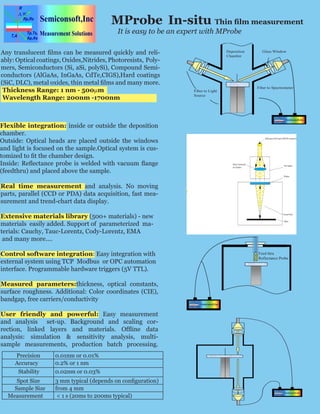
- 1. Precision 0.01nm or 0.01% Accuracy 0.2% or 1 nm Stability 0.02nm or 0.03% Spot Size 3 mm typical (depends on configuration) Sample Size from 4 mm Measurement < 1 s (20ms to 200ms typical) Flexible integration: inside or outside the deposition chamber. Outside: Optical heads are placed outside the windows and light is focused on the sample.Optical system is customized to fit the chamber design. Inside: Reflectance probe is welded with vacuum flange (feedthru) and placed above the sample. Feed thruReflectance Probe DepositionChamberGlass WindowFiber to SpectrometerFiber to Light Source Any translucent films can be measured quickly and reliably: Optical coatings, Oxides,Nitrides, Photoresists, Polymers, Semiconductors (Si, aSi, polySi), Compound Semiconductors (AlGaAs, InGaAs, CdTe,CIGS),Hard coatings (SiC, DLC), metal oxides, thin metal films and many more. Thickness Range: 1 nm - 500mm Wavelength Range: 200nm -1700nm Real time measurement and analysis. No moving parts, parallel (CCD or PDA) data acquisition, fast measurement and trend-chart data display. Extensive materials library (500+ materials) - new materials easily added. Support of parameterized materials: Cauchy, Tauc-Lorentz, Cody-Lorentz, EMA and many more.... Control software integration: Easy integration with external system using TCP Modbus or OPC automation interface. Programmable hardware triggers (5V TTL). Measured parameters:thickness, optical constants, surface roughness. Additional: Color coordinates (CIE), bandgap, free carriers/conductivity User friendly and powerful: Easy measurement and analysis set-up. Background and scaling correction, linked layers and materials. Offline data analysis: simulation & sensitivity analysis, multisample measurements, production batch processing. MProbe In-situ Thin film measurement It is easy to be an expert with MProbe
- 2. In-Situ System models Model Wavelength range Spectrometer/Detector/Light source Thickness range* VIS 400-1100 nm Spectrometer F4/Si 3600 pixels/ Tungsten - Halogen light source 15 nm to 20 mm (option:up to 50 mm) UVVisF 200-900 nm Spectrometer F4/ Si CCD 3600 pix-els/ Flash Xe light source 1 nm to 20 mm (option:up to 50 mm) HRVIS 700-1000 nm HR Spectrometer F4/Si 3600 pix-els/ Tungsten - Halogen light source 1 mm to 400 mm NIR 900-1700nm Transmission Spectrometer (TVG) F2/512 InGaAs/Tungsten-Halogen light source 100 nm-200 mm VISNIR 400-1700 nm Spectrometer F4 Si CCD 3600 pixels(Vis channel);Transmission Spectrometer (TVG)F2/512 InGaAs PDA( NIR channel) Tungsten-Halogen light source 15 nm to 200 mm UVVIS-NIR 200 -1700 nm Spectrometer F4 Si CCD 3600 pixels(Vis channel);Transmission (TVG) F2/512 InGaA ( NIR channel) Deuterium & Tungsten-Halogen light source 1 nm -200 mm XT 1590nm -1650nm Transmission Spectrometer (TVG) F2/512 InGaAs/Tungsten-Halogen light source 10 mm- 1 mm * T, n & k measurement in 40nm - 5mm thickness range Other configuration are available. OEM inquiries and custom development projects are welcome. One year limited warranty on labor and materials for all system. Semiconsoft, Inc, 2012 tel. +1.617.388.6832 email: info@semiconsoft.com fax.+1.508.858.5473 Visit us : http://www.semconsoft.com 1nm 10nm 100nm 1mm 100mm 1mm XT UVVISNIR VISNIR NIR HRVIS USVISSR 10mm