1. Footer Part: MYX7247S-QF883
Revision 1.1 - 09/13 1
LC2MOS Dual 12-Bit DAC
MYX7247S-QF883
Micross Components reserves the right to change products or specfications without notice
FEATURES
• Complete Dual 12-BIt DAC
• Two 12 Bit CMOS DAC’s
• On Chip Voltage Reference
• Output Amplifiers
• Reference Buffer Amplifiers
• Parallel Loading Structure
• Single or Dual Supply Operation
• Low Power - 165mW typ in Single Supply
LC2MOS
Dual 12-Bit DAC
28 LEAD CQFP
For more products and information
please visit our web site at
www.micross.com
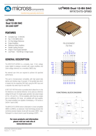
PIN ASSIGNMENT
(Top View)
4
NC
12
DB6
3
Voutb
13
DB5
2
Rofsb
14
DB4
1
REFOUT
15
DB3
28
REFIN
16
DB2
27
Rofsa
17
DB1
26
Vss
18
DB0
5DB11 25 Vouta
6DB10 24 Vdd
7NC 23 NC
8GND 22 WR/
9DB9 21 NC
10DB8 20 CSA/
11DB7 19 CSB/
MYX7247S-QF883
GENERAL DESCRIPTION
The MYX7247S-QF883 is a complete, dual, 12-bit, voltage
output digital to analogue converter with output amplifiers and
Zener voltage reference on a monolithic CMOS chip.
No external user trims are required to achieve full specified
performance.
This part is microprocessor compatible, with high speed data
latches and interface logic. It accepts 12 bit parrallel data which
is loaded into the respective DAC latch using the WR/ input and
a separate chip select input for each DAC.
A REF OUT/ REF IN function is provided which allows the on-chip
5V reference or an external reference to be used as a reference
voltage for the part.For single supply operation,two output ranges
of 0 to +5V and 0 to +10V are available, while these two ranges
plus an additional ±5V range are available with dual supplies.
The output amplifiers are capable of developing +10V across a
2kOhm load to GND.
The MYX7247S-QF883 silicon is fabricated in Linear compatible
CMOS (LC2MOS), an advanced, mixed technology process that
combines precision bipolar circuits with low power CMOS logic.
Packaged in a robust ceramic quad flat package (CQFP) .
FUNCTIONAL BLOCK DIAGRAM
2. Footer Part: MYX7247S-QF883
Revision 1.1 - 09/13 2
LC2MOS Dual 12-Bit DAC
MYX7247S-QF883
Micross Components reserves the right to change products or specfications without notice
ABSOLUTE MAXIMUM RATINGS*
VDD to GND -0.3V to
+17V
VDD to VSS: -0.3V to +34V
VOUTA
(note 1)
, VOUTB
(note 1)
to AGND (GND) -VSS -0.3V to VDD +0.3V
REFOUT(note 1)
to AGND (GND) 0V to VDD
REFINto AGND (GND) -0.3V to VDD +0.3V
Digital Inputs TO DGND (GND) -0.3V to VDD +0.3V
Operating temp range -55o
C to +125o
C
Storage temp range -65o
C to +150o
C
Lead soldering temp +300o
C
Power Disipation to +75o
C 1000mW
Derates above +75o
C by 9mW/o
C
* Stresses greater than those listed under “Absolute Maximum Ratings” may cause permanent damage to the device. This is a stress rating only and functional
operation of the device at these or any other conditions above those indicated in the operation section of this specification is not implied. Exposure to absolute
maximum rating conditions for extended periods may affect reliability.
Note 1:The outputs may be shorted to voltages in this range provided the power dissipation of the package is not exceeded. Short circuit current is typically 80mA.
THERMAL CHARACTERISTICS
Table 1: Thermal Resistances
Description Conditions SYM TYP MIN MAX Units Notes
Thermal Resistance Junction to Case ΘJC 28 - - o
C/W
Thermal Resistance Junction to Ambient ΘJA 96 - - o
C/W
SCREENING FLOW (IN ACCORDANCE WITH MIL-STD-883)
1. Temperature Cycle
2. Acceleration
3. Pre burn-in electrical test at ambient temperature
4. 160 hours burn-in
5. Post burn-in electrical test at ambient temperature. PDA: 10%
6. Electrical test at -55o
C. PDA: 10%
7. Electrical test at +125o
C
8. Fine & gross leak testing
9. Part marking
10. Lead forming
11. Parts to be solder dipped with PbSn (See mechnical definitions)
12. Final visual inspection.
Table 2: Sub Group testing
(Group A)
SUB GROUP Conditions
1 Static test @ +25o
C
2 Static test @ +125o
C
3 Static test @ -55o
C
9 Switching tests @ +25o
C
10 Switching test @ +125o
C
11 Swicthing tests @ -55o
C
3. Footer Part: MYX7247S-QF883
Revision 1.1 - 09/13 3
LC2MOS Dual 12-Bit DAC
MYX7247S-QF883
Micross Components reserves the right to change products or specfications without notice
STATIC CHARACTERISTICS
VDD = +15V (note 2) ±5%, VSS = 0V or -15V (note 2) ±5%, GND = 0V, REF IN = +5V RL = 2kΩ, CL=100pF.
All specifications Tmin to Tmax unless otherwise noted
Table 3: Electrical Specfications
Description Conditions Sub Group MIN MAX Units Notes
Resolution 1, 2, 3 12 12 Bits -
Relative Accuaracy 1, 2, 3 -1 +1 LSB max 3
Differenetial Nonlinearity Guranteed Monotonic 1, 2, 3 -0.9 +0.9 LSB max 3
Unipolar Offset Error
Vss=0V or -15V. DAC latch contents 0000
0000 0000
1, 2, 3 -3 3 LSB max 3
Bipolar Zero Error
Vss=-15V. DAC latch contents 1000 0000
0000
1, 2, 3 -4 +4 LSB max 3
Full Scale Error 1, 2, 3 -5 +5 LSB Max 4
Full Scale Mismatch -1 +1 Typ 4
REFOUT voltage 1, 2, 3 4.95 5.05 V
Reference temp coeffcient -25 +25 ppm/ o
C Typ
Reference load change (ΔREFOUT vs Δ1) Reference load current change (0 -100 μA) 1, 2, 3 -1 -1 mV
REFIN voltage 5V ± 1% 1, 2, 3 4.95 5.05 V
REFIN current -5 +5 μA 5
Digital Input high voltage 1, 2, 3 2.4 V
Digital Input low voltage 1, 2, 3 0.8 V
Digital input current IIN Data Inputs; VIN = 0V to VDD 1, 2, 3 -10 +10 μA
Digital input current IINH Control Inputs: VIN = VDD 1, 2, 3 -10 +10 μA
Digital input current IINL Control Inputs: VIN = 0V 1, 2, 3 - -150 μA
Input Capaciatnce - 16 pF
Output Range Resistors 1, 2, 3 15 30 k Ω
Output Voltage Ranges VSS=-15V, ROFSA = VOUTA, ROFSB = VOUTB 1, 2, 3 0 +5 V
Output Voltage Ranges VSS=-15V, ROFSA = REF IN, ROFSB = REF IN -5 +5 V
Output Voltage Ranges VSS=-15V, ROFSA = GND, ROFSB = GND 0 +10 V
Voltage output settling time
full scale change
VDD = +15V, VSS = -15V Settling to ± ½ LSB - 12 μS
Power Supply Current IDD Outputs Unloaded @ VDD= +15V & VSS=-15V 1, 2, 3 15 mA
Power Supply Current ISS Outputs Unloaded @ VDD= +15V & VSS=-15V 1, 2, 3 5 mA
4. Footer Part: MYX7247S-QF883
Revision 1.1 - 09/13 4
LC2MOS Dual 12-Bit DAC
MYX7247S-QF883
Micross Components reserves the right to change products or specfications without notice
DYNAMIC CHARACTERISTICS
VDD = +15V (note 2) ±5%, VSS = 0V or -15V (note 2) ±5%, GND = 0V, REF IN = +5V RL = 2kΩ, CL=100pF.
All specifications Tmin to Tmax unless otherwise noted
Table 4: Electrical Specfications Continued
Description SYM Conditions Sub Group MIN MAX Units Notes
CS/ to WR/ Setup Time t1
tR = tF = 5 ns 10% to 90% of 5V and timed
from voltage level 1.6V
9, 10, 11 0 ns
CS/ to WR/ Hold Time t2 9, 10, 11 0 ns
WR/ Pulse Width t3 9, 10, 11 150 ns
Data Valid to Write Setup Time t4 9, 10, 11 150 ns
Data Valid to Write Hold Time t5 9, 10, 11 15 ns
Address to Write Setup Time t6 9, 10, 11 0 ns
Address to Write Hold Time t7 9, 10, 11 0 ns
Table 5: Truth table
CSA/ CSB/ WR/ Function
x x 1 No Data Transfer
1 1 x No Data Transfer
0 1 0 DACA Latch Transparent
1 0 0 DACB Latch Transparent
0 0 0 Both DAC Latches Transparent
x = dont care.
5. Footer Part: MYX7247S-QF883
Revision 1.1 - 09/13 5
LC2MOS Dual 12-Bit DAC
MYX7247S-QF883
Micross Components reserves the right to change products or specfications without notice
ELECTRICAL CHARACTERISTICS NOTES
Note 2: Parts are functional at VDD +12V ±10% and VSS = 0V or -12V ±10%
Note 3: See terminology
Note 4: Measured with respect to REFIN and includes unipolar/bipolar offset error
Note 5: Sample tested at +25
o
C by die manufacturer to ensure compliance
PIN FUNCTION DESCRIPTION
Table 6: Pin Function
Package
Pin No
Mnemonic Description
1 REF OUT Voltage reference output. the internal 5V analogue reference is provided at this pin. To operate the part with internal reference,
REFOUT should be connected to REFIN
2 Rofsb Output offset resistor for the DAC B. This input configures the output ranges for DAC B it is connected to Voutb for the +5V
range to GND for the 10 V range and to REF IN for the ±5V range.
3 Voutb Analogue output voltage from DAC B. this is the buffer amplifier output voltage. Three different output voltage ranges can be
chosen: 0 to +5V, 0 to +10V and ±5V. The amplifier is capable of developing -10V across a 2kΩ
resistor to GND
4 NC No connection
5 DB11 Data Bit 11. Most significant bit (MSB)
6 DB10 Data Bit 10
7 NC No connection
8 GND Ground reference for all on chip circuity AGND and DGND too.
9 to 17 DB9-DB1 Data Bit 9 to Data Bit 1
18 DB0 Data Bit 0. Least significant bit (LSB)
19 CSB/ Chip select input for DAC B. Active low logic input. DAC B is selected when this input is active.
20 CSA/ Chip select input for DAC A. Active low logic input. DAC A is selected when this input is active.
21 NC No connection
22 WR/ Write input. WR/ is an active low logic input which is used in conjunction with CSA/ and CSB/ to write data to the DAC latches
23 NC No connection
24 Vdd Positive supply +15V
25 Vouta Analogue output voltage from DAC A. this is the buffer amplifier output voltage. Three different output voltage ranges can be
chosen: 0 to +5V, 0 to +10V and ±5V. The amplifier is capable of developing -10V across a 2kΩ
resistor to GND
26 Vss Negative supply -15V
27 Rofsa Output offset resistor for the DAC A. This input configures the output ranges for DAC A it is connected to Voutb for the +5V
range to GND for the 10 V range and to REF IN for the ±5V range.
28 REF IN Voltage reference input. The common reference voltage for both DAC’s is applied to this pin. It is internally buffered before
being applied to both DAC’s. The nominal reference voltage for correct operation of the MYX7247S-QP883 is 5V.
6. Footer Part: MYX7247S-QF883
Revision 1.1 - 09/13 6
LC2MOS Dual 12-Bit DAC
MYX7247S-QF883
Micross Components reserves the right to change products or specfications without notice
TERMINOLOGY
Relative accuracy or endpoint linearity is a measure of the maximum deviation of the DAC transfer function from a straight
line passing through the endpoints of the transfer function. It is measured after allowing for zero and full scale errors and is
expressed in LSB or as a percentage of full scale reading
Differential nonlinearity is the difference between the measured change and the ideal 1 LSB change between any two adja-
cent codes. A specified differential nonlinearity of ±1 LSB or less over the operating temperature range ensures monotonicity.
Single Supply linearity and gain error. The output amplifiers of the MYX7247S-QP883 can have negative offsets even when
the part is operated from a single+15V supply. However, because the negative supply rail (Vss) is 0V, the output cannot actually
go negative. Instead, when the output offset voltage is negative, the output voltage sits at 0V resulting in the transfer function
shown below. This Knee is an offset effect not a linearity error, and the transfer function would have followed the dotted line if
the voltage could have gone negative.
Normally, linearity is measured between zero and full scale after
offset and full scale have been adjusted, but this is not possible in
single supply operation if the offset is negative due to the knee in
the transfer fuction. Instead, linearity of the MYX7247S-QP883 in
the unipolar mode is measured between full scale and the lowest
code which is guaranteed to produce a positive output voltage. This
code is calculated from the maximum specification for negative
offset. i.e linearity is measured between codes 3 and 4095.
Unipolar offset error is the measured output voltage from VoutA or Vout B with all zeros loaded into the DAC latches when the
DAC’s are configured unipolar output it is a combination of the offset error of the DAC and the output amplifier
Bipolar zero error is the voltage measured at VoutA or Vout B when the DAC is connected in the bipolar mode and loaded with
code 2048. It is due to a combination of offset error in the DAC, amplifier offset and mismatch in the application resistors around
the amplifier.
7. Footer Part: MYX7247S-QF883
Revision 1.1 - 09/13 7
LC2MOS Dual 12-Bit DAC
MYX7247S-QF883
Micross Components reserves the right to change products or specfications without notice
MECHANICAL DEFINITIONS
Micross Case (Package Designator QF)
The component termination shall be solder dipped with standard PbSn solder to a depth of 0.6mm completely immersing the feet
of the device and shall meet the requirements of MIL-STD-883 Method 2003 or 2022. The test method to be identified on the
certificate of conformance. Solder finish on feet shall have a gold concentration not exceeding 0.2%.
MYX7247S-QF883
8. Footer Part: MYX7247S-QF883
Revision 1.1 - 09/13 8
LC2MOS Dual 12-Bit DAC
MYX7247S-QF883
Micross Components reserves the right to change products or specfications without notice
PCB FOOTPRINT DESIGN
Micross Case (Package Designator QF)
9. Footer Part: MYX7247S-QF883
Revision 1.1 - 09/13 9
LC2MOS Dual 12-Bit DAC
MYX7247S-QF883
Micross Components reserves the right to change products or specfications without notice
Document Title
MYX7247S-QF883
Revision History
Revision # History Release Date Status
1.0 Initial Release September 2013 Released