1. 1
Photocurrent on the edges of grapheme
Jakub Ondracek, Georgia Institute of Technology
Abstract
My project was focused on measuring an accumulation of charge on edges of grapheme. After building
all crucial parts to conduct the experiment, we did not get a positive result. On the other hand the project
shifted towards measuring photocurrent on the edges of grapheme. This phenomenon was detected and
additional experiments were conducted to analyze the photocurrent more accurately. The results showed
when a potential difference is applied while shining a laser on different parts of graphene, the maximum
current occurs while shining laser upon the edge. In addition, resist or air absorbents can be removed by
sufficiently high current flowing through a graphene sheet.
Preparation
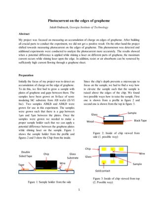
Initially the focus of my project was to detect an
accumulation of charge on the edge of graphene.
To do this, we first had to grow a sample with
plates of graphene and gaps between them. The
samples have been grown on Si-face of semi-
insulating SiC substrate from AB wafer (II-VI
Inc). Two samples ABKB and ABKD were
grown for use in this experiment. The samples
were grown such that there is a gap between
1µm and 5µm between the plates. Once the
samples were grown we needed to make a
proper sample holder such that we can apply a
potential difference between the graphene plates
while shining laser on the sample. Figure 1
shows the sample holder from the profile and
figures 2 and 3 show the Chip from the inside.
Figure 1: Sample holder from the side
Since the chip’s depth prevents a microscope to
focus on the sample, we had to find a way how
to elevate the sample such that the sample is
raised above the edges of the chip. We found
two possible ways how to raise the sample. First
one is shown from a profile in figure 2 and
second one is shown from the top in figure 3.
Figure 2: Inside of chip viewed from
side (1. possible way)
Figure 3: Inside of chip viewed from top
(2. Possible way)
Double
Sided Tape
Goldcontact
Sample
Gold contact
Glass
Wire
Chip
Wire
Tape
Chip Glass
Substrate
Sample
Glass
Black TapeWood
2. 2
First way of elevating the sample was to stack
small pieces of wood and glass and glue the
sample on top. However, while making the chip
this way, we found background noise of Raman
spectroscopy being increased by glue used to
attach the sample to the chip. In addition
background was increased by the piece of wood
used to elevate the sample. As the result the
black tape was used to eliminate the background
noise due to the wood. This way the chip was
usable and since we could access all contacts on
the chip, it was a viable option. However, we
have decided to use the second chip depicted in
figure 2 mainly for its simplicity and its
decreased possibility of background noise. In
this case the edges of the sample were glued to
the glass and the glass was glued to the edges of
the chip. The width of the glass was chosen to be
about the width of the sample and length a little
bit smaller than the length of the chip for
multiple reasons. The width of the glass should
be the width of the sample such that there is
enough space to wirebound the wires but the
glass has to be wide enough so the gluing of the
sample is as easy as possible. To cut the glass
the piece of glass we want to use is pressed
between two pieces of sharp metal with double
sided tape on them. Glass should be scratched by
a diamond and the scratch should align with the
two metal pieces. Force is then applied on the
rest of glass from the scratched side. The
technique to cut the glass is depictured in figure
4.
In the next stage of preparation, we had to
determine the state of all the devices on our
samples to see which ones can be used (see
figure 5). Once we found the working devices
we had to determine the voltage at which the
current starts to flow through the gap between
them so we know what voltage we should apply
to see the desired effect
Figure 4: Glass in a wise
Figure 5: One out of 4 structures on a
sample
Measurements
Once the sample holder was made and the
devices were analyzed, we have pursued to
measure the accumulation of charge on the
edges of graphene by detecting a shift in G peak
while applying potential difference to the
graphene plates. We did not detect any shift in
the peaks, but we noticed an IV curve change
while shining a laser on the edge of the
graphene. The change can be seen in figure 6.
Force applied
Double
Sided
Tape
Glass
Diamond
cut
Sharp
edge
metal
Gold
Contact Graphene
Device
3. 3
This shifted the focus of the project from
detection of accumulation of charge into
detection of photocurrent.
Figure 6: IV curve with laser on and off
Figure 7: IV curve of different positions
First we measured the current with voltage
ranging from -120V to 120V and the laser
turned on at selected positions on the sample.
All of the positions were spaced 0.2 µm or 0.5
µm on a single line covering two plates of
grapheme and a gap between them. The
resulting graph is shown in the figure 7. From
the figure you can see the current dependence on
the position of the laser which clearly shows the
appearance of the photocurrent.
After each measurement with laser on, we
measured the current at the same position and
conditions but with the laser turned off and the
results are shown in figure 8. This graph shows a
decrease of maximum current produced after
application of potential difference which might
suggest degradation of grapheme under the
relatively high voltage combined with the light
from the laser. However, this hypothesis was
later rejected when additional experiments were
done on the sample.
Figure 8: IV curve with laser off at
initial position (red) and position half
way though the scan (blue)
This degradation was also visible on the actual
sample. The gap has widened and it looked like
the graphene was damaged between the
electrodes. Figure 9a shows the initial state of
the device before an experiment and Figure 9b
shows the final state of the same device.
4. 4
Figure 9a: Device before a scan
Figure 9b: Device after a line scan with
a circle indicating the degradation of
graphene
To determine a state of the graphene after the
experiment, we mapped the device and looked at
the G peak and 2D peak. The map is shown in
figure 10. From the map we concluded that the
graphene itself was not damaged as previously
implied, but rather a resist or air absorbents on
the sample was affected.
Figure 10: Raman Spectroscopy map
after a scan. Figure a) showing G peak,
figure b) showing 2D peak.
To decrease the effects of current and light on
quality of the sample, we scanned focused laser
(1 μm in diameter) between the two contacts
while measuring Raman spectra to detect
position of graphene sheets. The photocurrent
was measured simultaneously while constant
bias was applied between the two contacts. We
again measured the intensity of G peak, but this
time we measured current as function of position
of the laser as well. Figure 11 shows the
intensity of G peak in upper figure and current
as a function of position of the laser in the lower
figure. Both graphs were normalized such that a
vertical line can show a relationship between the
intensity of G peak and current at given point.
a)
b)
5. 5
Figure 11: Upper figure shows the G
peak intensity and the bottom figure
shows the current at given position
Figure 11 shows another interesting
phenomenon as the peak of the current is at a
beginning of the edge. It is hard to say why the
peak of the current is at the bottom of the edge
rather than in the middle. It might be due to the
laser shining on the most outer edge and therefor
creating free charges the closest to the other
graphene, but more experiments need to be done
to determine the cause of this phenomenon.
Conclusion
Even though we did not get to measure an
accumulation of charge on the edge of graphene,
we found that there is a photocurrent produced
at the edge of the graphene when a laser is
shined on it. Further analysis has shown that
resist or air absorbents on graphene can be
eliminated by high enough current flowing
through a sample which decreases graphene’s
electric capabilities.