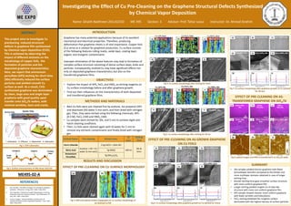
1. Investigating the Effect of Cu Pre-Cleaning on the Graphene Structural Defects Synthesized
by Chemical Vapor Deposition
Name: Ghaith Nadhreen 201142310 ME 495 Section: 3 Advisor: Prof. Tahar Laoui Instructor: Dr. Ahmad Ibrahim
INTRODUCTION
EFFECT OF PRE-CLEANING ON AS-GROWN GRAPHENE
ON CU FOILS
ABSTRACT
METHODS AND MATERIALS
SUMMARY
This project aims to Investigate Cu
precleaning -induced structural
defects in graphene film synthesized
by chemical vapor deposition (CVD).
This is achieved by observing the
impact of different etchants on the
morphology of copper foils, the
formation of particles and the
deposited graphene characteristics.
Here, we report that ammonium
persulfate (APS) etching for short time
(30s) efficiently reduced the surface
particles and yielded smooth Cu
surface as well. As a result, CVD-
synthesized graphene was dominated
by clean, large area and single layer
graphene with good quality upon
transfer onto SiO2/Si wafers, with
minimal wrinkles, tears and cracks. • Bare-Cu foils were pre-cleaned first by acetone, Iso-propanol (ISP)
and deionized (DI) water 5 min each, and then dried with nitrogen
gas. Then, they were etched using the following chemicals; APS
(0.3 M), FeCl3 (1M) and HNO3 (1M).
• Cu samples were etched for 30s, and 5 min to achieve slight and
harsh cleaning conditions.
• Then, Cu foils were cleaned again with DI water for 5 min to
remove any etchants contaminants and finally dried with nitrogen
gas.
• 30s samples yielded thinner graphene with fewer
bi/multilayer domains compared to the thicker and
more multilayer domains obtained in case of longer
etching time
• Shorter etching time gave smoother surface structure
with more uniform graphene film
• Longer etching yielded rougher Cu of step-like
structure with more non-uniform graphene film
• APS sample showed cleaner, more uniform graphene
with fewer wrinkles and holes/pores
• FeCl3 etching exhibited the roughest surface
dominated with the highest density of surface particles
Graphene has many potential applications because of its excellent
mechanical and electrical properties. Therefore, producing
deformation free graphene sheets is of vital importance. Copper foils
(Cu) serve as a catalyst for graphene production. Cu surface consists
of the following features rolling marks, oxide layer, coating layer,
organic and inorganic contaminants.
Improper elimination of the above features may lead to formation of
complex surface structure consisting of dense surface steps, kinks and
particles. Consequently, evolved Cu may have significant effects not
only on deposited graphene characteristics but also on the
transferred graphene films.
OBJECTIVES
• Explore the impact of APS, FeCl3 and HNO3 as etching reagents on
Cu surface morphology before and after graphene growth.
• Find out their influences on the characteristics of both deposited
and transferred graphene films.
Etchant Name Pre-cleaning Etchant conc.
DI
conc.
Etching
Time
Ferric Chloride
Acetone + ISP + D.I
water (5 min each)
3.5g FeCl3 + 10ml HCl
100 ml
30s &
5min
Nitric Acid 7g HNO3
Ammonium
Persulfate
7g (NH4)2S2O8
EFFECT OF PRE-CLEANING ON CU SURFACE MORPHOLOGY
50 m
(a) RMS = 360 nm
20 m
(b)
Fig 3: SEM and optical surface topography for Cu surface morphology of
as-received Cu foil
(e)
5 m
(d) (f)Cu-FeCl3-5min Cu-HNO3-5minCu-APS-5min
RMS= 517 nm RMS= 573 nm RMS= 337 nm(a) (b) (c)
Cu-FeCl3-5min Cu-HNO3-5minCu-APS-5min
Fig 4: Cu surface morphology after etching for 5min
Cu-APS-30s(d) Cu-FeCl3-30s(e) Cu-HNO3-30s(f)
5 m
Cu-APS-30s Cu-FeCl3-30s
RMS= 421 nm RMS= 524 nm RMS= 326 nm
Cu-HNO3-30s
(a) (b) (c)
Fig 5: Cu surface morphology after etching for 30 sec
(b) G/Cu-FeCl3-5min (c) G/Cu-HNO3-5min
20 µm
(a) G/Cu-APS-5min
1200 1400 1600 1800 2000 2200 2400 2600 2800
0
50
100
150
200
250
300
1200 1400 1600 1800 2000 2200 2400 2600 2800
0
50
100
150
200
250
1200 1400 1600 1800 2000 2200 2400 2600 2800
0
50
100
150
200
250
(e)
G/Cu-FeCl3-5min
(f)
G/Cu-HNO3-5min
(d)
G/Cu-APS-5min
(h) (i)(g)
Raman shift (cm-1) Raman shift (cm-1) Raman shift (cm-1)
Intensity(a.u)
Intensity(a.u)
Intensity(a.u)
Fig 6: Cu surface morphology after graphene growth on Cu (etched for 5min)
(d) (e) (f)G/Cu-APS-30s G/Cu-FeCl3-30s G/Cu-HNO3-30s
G/Cu-APS-30s(a) G/Cu-FeCl3-30s(b) G/Cu-HNO3-30s(c)
1000 1200 1400 1600 1800 2000 2200 2400 2600 2800 3000
0
20
40
60
80
100
120
140
160
180
200
1000 1200 1400 1600 1800 2000 2200 2400 2600 2800 3000
0
50
100
150
200
250
1000 1200 1400 1600 1800 2000 2200 2400 2600 2800 3000
0
50
100
150
200
250
(g) (h) (i)
Raman shift (cm-1) Raman shift (cm-1) Raman shift (cm-1)
Intensity(a.u)
Intensity(a.u)
Intensity(a.u)
Fig 7: Cu surface morphology after graphene growth on Cu (etched
for 30 sec)
EFFECT OF PRE-CLEANING ON AS-
TRANSFERRED GRAPHENE ON SIO2/SI
(g) (i)(h)
G/SiO2-APS-30s G/SiO2-FeCl3-30s G/SiO2-HNO3-30s
(d) (e) (f)G/SiO2-APS-
5min
G/SiO2-FeCl3-
5min
G/SiO2-HNO3-5min
G/SiO2-APS-
30s
(a) G/SiO2-
FeCl330s
(b) G/SiO2-
HNO330s
(c)
20
µm
Fig 8: optical images and AFM of transferred G on SiO2/Si wafer
1
2 3
2
4
4
1- Adsorption 2- Diffusion 3- Attachment 4- Desorption
Quartz Tube
Ar+H2+CH4
1000 oC
Cu
Cu foil
OrganicInorganic Coating
layer
Oxide
layer
Fig 1: CVD schematics
Fig 2: Surface characteristics of Alfa Aesar (AA) foil
REFERENCES
1. Kim, Soo Min. "The Effect of Copper Pre-cleaning on Graphene
Synthesis." IOPscience. 13 Aug. 2013. Web. 2 May 2016.
2. Han, Gang Hee. "Influence of Copper Morphology in Forming
Nucleation Seeds for Graphene Growth." ACS Publications. 24
Aug. 2011. Web. 2 May 2016.
3. Lupina, Grzegorz. "Residual Metallic Contamination of
Transferred Chemical Vapor Deposited Graphene." ArXiv. 2015.
Web. 2 May 2016.
ME495-02-A
RESULTS AND DISCUSSION