qsfp-40g-lr4-10km-optical-module-121002.pdf
•
0 likes•2 views

40G 1310nm 10km QSFP+ LR4 Transceiver

Recommended
Recommended
More Related Content
Similar to qsfp-40g-lr4-10km-optical-module-121002.pdf
Similar to qsfp-40g-lr4-10km-optical-module-121002.pdf (20)
More from GLsun Mall
More from GLsun Mall (20)
Recently uploaded
Recently uploaded (20)
qsfp-40g-lr4-10km-optical-module-121002.pdf
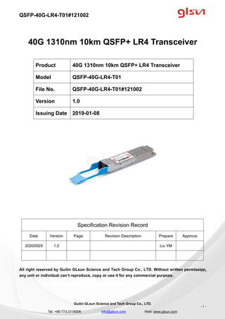
- 1. QSFP-40G-LR4-T01#121002 Guilin GLsun Science and Tech Group Co., LTD. Tel: +86-773-3116006 info@glsun.com Web: www.glsun.com - 1 - 40G 1310nm 10km QSFP+ LR4 Transceiver Specification Revision Record Date Version Page Revision Description Prepare Approve 20200929 1.0 Liu YM All right reserved by Guilin GLsun Science and Tech Group Co., LTD. Without written permission, any unit or individual can’t reproduce, copy or use it for any commercial purpose. Product 40G 1310nm 10km QSFP+ LR4 Transceiver Model QSFP-40G-LR4-T01 File No. QSFP-40G-LR4-T01#121002 Version 1.0 Issuing Date 2019-01-08 - 1 -
- 2. QSFP-40G-LR4-T01#121002 Guilin GLsun Science and Tech Group Co., LTD. Tel: +86-773-3116006 info@glsun.com Web: www.glsun.com - 2 - Product Feature 4 CWDM lanes MUX/DEMUX design 4 independent full-duplex channels up to 11.3Gbps data rate per wavelength Hot-pluggable QSFP +footprint RoHS compliant and Lead Free Up to 10Km link length Power dissipation <3.5W (0~70℃) Commercial operating temperature optional Compliant with IEEE802.3ba, SFF-8436 Application 40G Ethernet Infiniband 4X SDR DDR QDR 40G Telecom connections Regulatory Compliance ESD to the Electrical PINs: compatible with MIL-STD-883 Method 3015 ESD to the Duplex LC Receptacle: compatible with IEC 61000-4-2 Immunity compatible with IEC 61000-4-3 EMI compatible with FCC Part 15 Class B EN55022 Class B (CISPR 22B) VCCI Class B Laser Eye Safety compatible with FDA 21CFR 1040.10 and 1040.11 EN60950, EN (IEC) 60825-1,2 RoHS compliant with RoHS 2 (2011/65/EU) Absolute Maximum Ratings Parameter Symbol Min Typ Max Unit Ref. Maximum Supply Voltage Vcc -0.5 +4.0 V Storage Temperature TS -40 +85 °C Operating Humidity RH 0 85 % Recommended Operating Conditions Parameter Symbol Min Typ Max Unit Ref. Power Supply Voltage Vcc 3.13 3.30 3.47 V Power Supply Current Icc - - 1.1 A Commercial Case Operating Temperature Tc 0 +70 °C Commercial Bit Rate Each Lane Br 1 11.3 Gbps 9/125um G.652 SMF Lmax - - 10 km
- 3. QSFP-40G-LR4-T01#121002 Guilin GLsun Science and Tech Group Co., LTD. Tel: +86-773-3116006 info@glsun.com Web: www.glsun.com - 3 - Electrical Characteristics (TOP=25°C, Vcc=3.3Volts) Optical Characteristics (TOP=25°C, Vcc=3.3 Volts) Parameter Symbol Min Typ Max Unit Ref. Transmitter Input differential impedance Rin 85 100 120 Ω 1 Differential data input swing Vin, pp 120 - 850 mV TX Disable-High - Vcc-0.8 - Vcc V TX Disable-Low - Vee - Vee+0.8 V TX Fault-High - Vcc-0.8 - Vcc V TX Fault-Low - Vee - Vee+0.8 V Receiver Single ended data output swing Vout, pp 300 - 850 mV 2 Data output rise time Tr 30 ps 3 Data output fall time Tf 30 ps 3 LOS-High - Vcc-0.8 Vcc V LOS-Low - Vee Vee+0.8 V Notes: 1. AC coupled. 2. Into 100 ohm differential termination. 3. 20-80% Parameter Symbol Min Typ Max Unit Ref. Transmitter Center wavelength L0 1264.5 1271 1277.5 nm L1 1284.5 1291 1297.5 nm L2 1304.5 1311 1317.5 nm L3 1324.5 1331 1337.5 nm Side-mode Suppression Ratio SMSR 30 dB Total Average Launch Power PT 8.3 dBm Average Launch Power, each Lane -7 2.3 dBm
- 4. QSFP-40G-LR4-T01#121002 Guilin GLsun Science and Tech Group Co., LTD. Tel: +86-773-3116006 info@glsun.com Web: www.glsun.com - 4 - Pin Descriptions Pin Symbol Name/Description Ref. 1 GND Ground 2 Tx2n Transmitter Inverted Data Input, CML-I 3 Tx2p Transmitter Non-Inverted Data output, CML-I 4 GND Ground 5 Tx4p Transmitter Inverted Data Input, CML-I 6 NGD Transmitter Non-Inverted Data output, CML-I 7 GND GND 8 ModSeIL The ModSelL is an input pin. When held low by the host, the module responds to 2-wire serial communication commands. The ModSelL allows the use of multiple QSFP+ modules on asingle 2-wire interface bus. When the ModSelL is “High”, the module shall not respond to or acknowledge any 2-wire interface communication from the host. ModSelL signal input node must be biased to the “High” state in the module Optical Modulation Amplitude, each Lane OMA -4 3.5 dBm Extinction Ratio ER 3.5 dB TDP, each lane TDP 2.3 dB Relative Intensity Noise RIN -128 dB/Hz Transmitter Reflectance RT -12 dB Receiver RX Sensitivity @10.3Gb/s, each lane SENS - - -11.5 dBm 1 Receiver Overload 2.3 - - dBm Difference in Receive Power between any two Lanes (OMA) 7.5 dB LOS De-Assert LOSD - -12 dBm LOS Assert LOSA -25 - dBm LOS Hysteresis 0.5 - dB Notes: 1.Measured with conformance signals defined in FC-PI-2 Rev. 10.0 specifications. 2.Measured with PRBS 231 -1 at 10-12 BER.
- 5. QSFP-40G-LR4-T01#121002 Guilin GLsun Science and Tech Group Co., LTD. Tel: +86-773-3116006 info@glsun.com Web: www.glsun.com - 5 - 9 ResetL The ResetL pin must be pulled to Vcc in the QSFP+ module. A low level on the ResetL pin for longer than the minimum pulse length (t_Reset_init) initiates a complete module reset, returning all user module settings to their default state. Module Reset Assert Time (t_init) starts on the rising edge after the low level on the ResetL pin is released. 10 VccRx ﹢3.3V Power Supply Receiver 11 SCL 2-Wire Serial Interface Clock 12 SDA 2-Wire Serial Interface Data 13 GND GND 14 Rx3p Receiver Non-Inverted Data Output, CML-O 15 Rx3n Receiver Inverted Data Output, CML-O 16 GND GND 17 Rx1p Receiver Non-Inverted Data Output, CML-O 18 Rx1n Receiver Inverted Data Output, CML-O 19 GND Ground 20 GND Ground 21 Rx2n Receiver Inverted Data Output, CML-O 22 Rx2p Receiver Non-Inverted Data Output, CML-O 23 GND Ground 24 Rx4n Receiver Inverted Data Output, CML-O 25 Rx4p Receiver Non-Inverted Data Output, CML-O 26 GND Ground 27 ModPrsL Module Present, connect to GND 28 IntL The IntL pin is an open collector output and must be pulled to host supply voltage on the host board. The INTL pin is de-asserted “High” after completion of reset, when byte 2 bit 0 (Data Not Ready) is read with a value of ‘0’ and the flag field is read. 29 VccTx +3.3 V Power Supply transmitter 30 Vcc1 +3.3 V Power Supply 31 LPMode The LPMode pin shall be pulled up to Vcc in the QSFP+ module. This function is affected by the LPMode pin and the combination of the Power_over-ride and Power_set software control bits (Address A0h, byte 93 bits 0,1). 32 GND Ground 33 Tx3p Transmitter Non-Inverted Data Input, CML-I
- 6. QSFP-40G-LR4-T01#121002 Guilin GLsun Science and Tech Group Co., LTD. Tel: +86-773-3116006 info@glsun.com Web: www.glsun.com - 6 - 34 Tx3n Transmitter Inverted Data Output, CML-I 35 GND Ground 36 Rx1p Transmitter Non-Inverted Data Input, CML-1 37 Rx1n Transmitter Inverted Data Output, CML- 38 GND Ground Pin-out of Connector Block on Host Board
- 7. QSFP-40G-LR4-T01#121002 Guilin GLsun Science and Tech Group Co., LTD. Tel: +86-773-3116006 info@glsun.com Web: www.glsun.com - 7 - Recommend Circuit Schematic
- 8. QSFP-40G-LR4-T01#121002 Guilin GLsun Science and Tech Group Co., LTD. Tel: +86-773-3116006 info@glsun.com Web: www.glsun.com - 8 - Mechanical Specifications
- 9. QSFP-40G-LR4-T01#121002 Guilin GLsun Science and Tech Group Co., LTD. Tel: +86-773-3116006 info@glsun.com Web: www.glsun.com - 9 - EEPROM Information EEPROM memory map specific data field description is as below:
- 10. QSFP-40G-LR4-T01#121002 Guilin GLsun Science and Tech Group Co., LTD. Tel: +86-773-3116006 info@glsun.com Web: www.glsun.com - 10 - Digital Diagnostic Monitoring Interface Parameter Range Accuracy Calibration Temperature 0 to +70°C ±3°C Internal Voltage 2.97 to 3.63V ±3% Internal Bias Current 0 to 100mA ±10% Internal Rx Power -12 to 2.5dBm ±3dB Internal Ordering Information Part Number Operating Case temperature DDMI QSFP-40G-LR4-T01 Commercial(0~70℃) Yes