SlideShare a Scribd company logo
1 of 64
Download to read offline
Version	
  11.0	
  	
  Updated	
  November	
  30,	
  2015	
  
•  Linux	
  log	
  in	
  and	
  tutorial	
  
•  Synthesis	
  with	
  dc_shell	
  
•  Timing	
  	
  
•  Area	
  
•  Chip	
  implementaEon	
  with	
  icc_shell	
  
•  Placement	
  
•  RouEng	
  
•  Clock	
  tree	
  
•  Finishing	
  
•  Chip	
  tesEng	
  and	
  verificaEon	
  with	
  cdesigner	
  	
  
•  Design	
  Rules	
  Checks	
  (DRC)	
  
•  Layout	
  Versus	
  SchemaEc	
  (LVS)	
  
•  MOSIS	
  submission	
  
Synopsys	
  ASIC	
  Tutorial	
  
ssh	
  allows	
  us	
  to	
  login	
  to	
  the	
  system	
  and	
  	
  
“-­‐X”	
  enables	
  X	
  Windows	
  support	
  
Quick	
  Linux	
  Tutorial	
  
You	
  are	
  expected	
  to	
  have	
  a	
  working	
  
knowledge	
  of	
  Linux	
  for	
  this	
  lab.	


“pwd”	
  –	
  print	
  working	
  directory	
  –	
  should	
  be	
  
your	
  user	
  directory	
  
“cd”	
  –	
  change	
  directory	
  into	
  
reference_design.	


“ls	
  –alrt”	
  –	
  list	
  directory	
  contents.	


Other	
  useful	
  Linux	
  commands:	
  
	
  man	
  –	
  help	
  for	
  commands	


  top	
  
	
  mkdir	
  
	
  passwd	
  
	
  cd	
  ~	


  cd	
  ..	


  rm	
  
	
  grep	
  
	
  more	
  
	
  cat	


Type	
  xclock	
  and	
  you	
  should	
  see	
  a	
  clock	
  
appear	
  if	
  X	
  Windows	
  is	
  working	
  properly	
  	
  -­‐	
  
shown	
  on	
  your	
  screen	
  but	
  running	
  remotely.	
  
Log	
  in	
  with	
  Linux	
  
cd	
  /opt/eda/synopsys/local/ON.PDK	
  	
  	
  (University	
  specific	
  –	
  ask	
  administrator)	


cp	
  	
  	
  –r	
  	
  reference_design/	


  ~/.	
  
This	
  will	
  create	
  a	
  directory	
  structure.	


cd	
  ~/reference_design	


RTL	
  is	
  where	
  you	
  should	
  store	
  your	
  source	
  verilog	
  code.	


SYN	
  is	
  where	
  you	
  will	
  perform	
  synthesis.	
  	
  	
  Update	
  the	
  script	
  “dc_good.tcl”	
  in	
  scripts	
  
and	
  invoke	
  “dc_shell	
  –f	
  dc_good.tcl	
  |	
  tee	
  logs/output.syn”	


PNR	
  is	
  where	
  you	
  will	
  perform	
  place	
  and	
  route.	
  	
  Update	
  the	
  script	
  “icc_good.tcl”	
  in	
  
scripts	
  and	
  invoke	
  “ic_shell	
  –f	
  icc_good.tcl	
  |	
  tee	
  logs/output.ic”	


CUSTOM	
  is	
  where	
  you	
  store	
  reference	
  files.	
  Eg:	
  matlab	
  files	
  that	
  create	
  test	
  vectors	
  
and	
  expected	
  results,	
  simulaEon	
  will	
  use	
  these	
  vectors	
  and	
  match	
  the	
  results.	


SIM	
  is	
  where	
  you	
  store	
  your	
  simulaEon	
  files.	
  	
  OpEonal	
  in	
  this	
  case.	


GOLDEN	
  is	
  where	
  you	
  store	
  your	
  final	
  files	
  –	
  RTL,	
  GDS,	
  SDC,	
  TB.v,	
  and	
  scripts.	
  
Copy	
  the	
  Reference	
  Design	
  
logs/output.dc?	
  Or	
  outpu
Simple	
  reference	
  design	
  
Two	
  counters	
  –	
  one	
  clocked	
  by	
  external	
  
clock,	
  the	
  other	
  by	
  an	
  internally	
  
generated	
  clock.	
  	
  All	
  clocks	
  have	
  to	
  be	
  
idenEfied	
  for	
  staEc	
  Eming	
  to	
  work	
  
correctly.	
  	
  	
  Total	
  of	
  40	
  flip-­‐flops	
  no	
  
where	
  near	
  the	
  limit	
  in	
  terms	
  of	
  area	
  
for	
  this	
  chip	
  size.	


Only	
  four	
  outputs	
  and	
  two	
  inputs,	
  
power	
  and	
  ground.	
  	
  Total	
  is	
  8	
  pins.	
  
Design	
  Compiler	
  -­‐	
  Reference	
  Design	
  	
  
cd	
  to	
  syn	
  directory	
  for	
  synthesis	
  
cd	
  syn	
  
Edit	
  and	
  update	
  the	
  script	
  “dc_good.tcl”	
  for	
  your	
  specific	
  design	
  
	
  idenEfy	
  file	
  and	
  module	
  name	
  
	
  idenEfy	
  clocks	
  and	
  frequency	
  
source	
  /opt/eda/synopsys/synopsys.cshrc-­‐20151021	
  (university	
  specific	
  –	
  ask	
  admin)	
  
Run	
  “dc_shell	
  –f	
  ”	
  to	
  invoke	
  script	
  as	
  shown	
  above	
  in	
  shell.	
  
Look	
  in	
  reports	
  for	
  quality	
  of	
  output	
  by	
  reading	
  area	
  and	
  Eming	
  reports.	


The	
  tool	
  can	
  be	
  opened	
  in	
  gui	
  format	
  as	
  well	
  –	
  “dc_shell	
  –gui”	
  although	
  synthesis	
  is	
  
tradiEonally	
  done	
  with	
  a	
  script	
  only.	
  
Design	
  Compiler	
  -­‐	
  Prepare	
  for	
  synthesis	
  
Design	
  Compiler	
  -­‐	
  Checking	
  synthesis	
  
During	
  synthesis	
  you	
  should	
  see	
  standard	
  output.	


Flip-­‐flops	
  will	
  be	
  idenEfied.	
  	
  Make	
  sure	
  this	
  make	
  sense.	
  	
  I	
  have	
  two	
  20	
  bit	
  
counters	
  in	
  the	
  reference	
  design	
  so	
  this	
  report	
  looks	
  reasonable.	


Also	
  look	
  for	
  latches	
  which	
  indicates	
  a	
  problem	
  in	
  your	
  RTL.	
  	
  All	
  if	
  statements	
  
need	
  an	
  else	
  and	
  if	
  missing	
  can	
  cause	
  latches.	
  
Aier	
  script	
  is	
  run,	
  look	
  for	
  return	
  values	
  of	
  1	
  for	
  all	
  lines.	
  0	
  is	
  a	
  failure	
  for	
  the	
  command.	
  
In	
  results	
  you	
  will	
  have	
  a	
  *postsynth.v	
  as	
  your	
  netlist	
  and	
  a	
  sdc	
  file	
  with	
  Eming	
  info.	
  
Check	
  the	
  netlist	
  to	
  make	
  sure	
  it	
  looks	
  reasonable.	
  
In	
  logs,	
  you	
  will	
  see	
  the	
  commands	
  and	
  output.	
  	
  Search	
  for	
  errors	
  and	
  “0’s”.	
  
In	
  reports,	
  check	
  all	
  files	
  thoroughly.	
  
	
  Timing	
  –	
  check	
  that	
  criEcal	
  path	
  passes	
  and	
  is	
  legiEmate.	
  
	
  Area	
  –	
  not	
  too	
  big.	
  	
  I	
  will	
  report	
  numbers	
  that	
  are	
  reasonable	
  in	
  class.	
  
	
  Power	
  is	
  interesEng	
  but	
  not	
  very	
  accurate.	
  	
  Power	
  is	
  data	
  dependent	
  but	
  you	
  can	


  improve	
  by	
  adding	
  switching	
  data	
  from	
  the	
  simulator	
  VCS.	
  
Design	
  Compiler	
  -­‐	
  AHer	
  synthesis	
  
Final	
  Report:	
  Add	
  Lming	
  and	
  
area	
  reports	
  to	
  final	
  report.	
  
Design	
  Compiler	
  -­‐	
  Checking	
  synthesis	
  
Top	
  of	
  the	
  netlist	
  should	
  have	
  your	
  module	
  name,	
  IO’s	
  and	
  nets.	


You	
  will	
  see	
  some	
  starEng	
  with	
  a	
  back	
  slash	
  which	
  is	
  an	
  escape	
  character	
  as	
  
some	
  tools	
  cannot	
  handle	
  square	
  brackets	
  and	
  this	
  character	
  is	
  used	
  to	
  escape.	
  
Design	
  Compiler	
  -­‐	
  Checking	
  synthesis	
  
Tri’s	
  will	
  be	
  inserted	
  due	
  to	
  the	
  IO’s	
  being	
  bidirecEonal.	


Also,	
  look	
  at	
  the	
  gates.	
  	
  DCX1	
  is	
  a	
  flip-­‐flop.	
  	
  Scroll	
  down	
  to	
  check	
  all	
  of	
  the	
  gates.	
  
Design	
  Compiler	
  -­‐	
  Checking	
  synthesis	
  
Pad_bidirhe	
  are	
  the	
  IO	
  cells	
  and	
  you	
  should	
  see	
  other	
  gates	
  like	
  NAND2X1.	


NAND2X1	
  is	
  the	
  smallest	
  2	
  input	
  NAND	
  gate.	
  	
  X1	
  means	
  small	
  and	
  the	
  2	
  is	
  the	
  
number	
  of	
  inputs.	
  	
  	
  A	
  and	
  B	
  are	
  in	
  and	
  Y	
  is	
  the	
  output	
  pins	
  normally.	
  
Design	
  Compiler	
  -­‐	
  Timing	
  report	
  
Worse	
  case	
  path	
  for	
  main	
  clock.	


Through	
  the	
  adder	
  from	
  bit	
  0	
  to	
  bit	
  19	
  
as	
  expected.	
  	
  20	
  nS	
  to	
  complete	
  and	
  
finished	
  in	
  8.34	
  nS	
  so	
  Eme	
  to	
  spare	
  –	
  
which	
  means	
  posiEve	
  slack	
  of	
  11.27	
  nS.	


Passed	
  and	
  made	
  sense.	
  Note	
  that	
  
these	
  Emings	
  are	
  only	
  for	
  setup	
  
calculaEons	
  and	
  no	
  holds	
  are	
  
completed.	
  	
  Since	
  the	
  clock	
  tree	
  is	
  not	
  	
  
in	
  place	
  (ideal	
  clock	
  tree	
  assumed)	
  
there	
  is	
  no	
  clock	
  skew	
  which	
  is	
  required	
  
for	
  hold	
  violaEons.	


Final	
  Report:	
  Add	
  Lming	
  
report	
  to	
  final	
  report.	
  
Check	
  for	
  latches	
  (should	
  not	
  exist)	
  and	
  that	
  the	
  basic	
  numbers	
  are	
  reasonable.	


For	
  the	
  MOSIS	
  chip,	
  I	
  expect	
  that	
  3-­‐5	
  Emes	
  this	
  area	
  is	
  possible,	
  so	
  500,000	
  square	
  microns	
  
should	
  fit	
  in	
  the	
  allocated	
  space.	
  
Design	
  Compiler	
  -­‐	
  Area	
  report	
  
Final	
  Report:	
  Add	
  area	
  
report	
  to	
  final	
  report.	


IC	
  Compiler	
  -­‐	
  Place,	
  route,	
  Lming	
  and	
  checks	
  
The	
  icc_good.tcl	
  script	
  will	
  go	
  into	
  the	
  synthesis	
  directory	
  
to	
  obtain	
  the	
  netlist	
  and	
  sdc	
  file	
  (Eming).	


Note	
  that	
  the	
  script	
  has	
  commented	
  lines	
  indicaEng	
  
different	
  secEons	
  of	
  the	
  script	
  that	
  will	
  be	
  run	
  piecemeal.	
  
The	
  command	
  “return”	
  will	
  stop	
  the	
  script	
  and	
  is	
  used	
  to	
  
run	
  to	
  a	
  specific	
  locaEon.	
  
IC	
  Compiler	
  –	
  First	
  return	
  –	
  Floor	
  Plan	
  
Run	
  to	
  first	
  “return”	
  in	
  script	
  –	
  start_gui	
  to	
  invoke	
  viewer.	


You	
  will	
  need	
  to	
  run	
  to	
  this	
  point	
  twice:	
  once	
  just	
  to	
  create	
  an	
  IO	
  file	
  and	
  a	
  second	
  Eme	
  
using	
  the	
  IO	
  file	
  file	
  with	
  the	
  line	
  “source	
  is_pad.tcl”	
  uncommented.	


Run	
  the	
  first	
  Eme	
  and	
  change	
  the	
  IO	
  file	
  name	
  of	
  a	
  newly	
  created	
  file:	
  	
  
cp	
  set_pad_apributes_on_cell_xtal_chip_with_io.tcl	
  	
  is_pad.tcl	


Check	
  that	
  the	
  file	
  has	
  all	
  IO	
  declared.	


Uncomment	
  the	
  “source	
  is_pad.tcl”	
  line	
  in	
  the	
  script	
  and	
  run	
  again.	
  
IC	
  Compiler	
  –	
  First	
  return	
  –	
  Floor	
  Plan	
  
IC	
  Compiler	
  –	
  First	
  return	
  –	
  Floor	
  Plan	
  
Use	
  the	
  ruler	
  to	
  check	
  sizes	
  of	
  the	
  die.	
  	
  1500	
  microns	
  is	
  the	
  max	
  size	
  for	
  each	
  side.	


IC	
  Compiler	
  –	
  First	
  return	
  –	
  Floor	
  Plan	
  
Change	
  the	
  visibility	
  selecEons	
  to	
  see	
  different	
  layers.	
  	
  Pins	
  and	
  Site	
  rows	
  to	
  see	
  metals	
  and	
  
where	
  the	
  standard	
  cells	
  will	
  be	
  placed	
  later.	


Note	
  that	
  all	
  unplaced	
  cells	
  are	
  to	
  the	
  right	
  –	
  out	
  of	
  bounds	
  for	
  now.	


Final	
  
Report:	
  Add	
  
screen	
  shot	
  
to	
  final	
  
report.	


IC	
  Compiler	
  Second	
  return	
  –	
  Power	
  and	
  IO	
  Fill	
  
IC	
  Compiler	
  Second	
  return	
  –	
  Power	
  and	
  IO	
  Fill	
  
Should	
  see	
  power	
  lines	
  at	
  all	
  three	
  levels	
  and	
  ring	
  with	
  verEcal	
  straps.	
  	
  IO	
  Ring	
  is	
  complete	
  
but	
  you	
  must	
  set	
  the	
  visual	
  seqngs	
  to	
  “Max	
  Quality”.	
  	
  Change	
  levels	
  to	
  1	
  or	
  2	
  to	
  see	
  into	
  
lower	
  hierarchical	
  levels.	
  	
  May	
  need	
  to	
  change	
  color	
  of	
  poly	
  to	
  see	
  transistors.	
  
IC	
  Compiler	
  Third	
  Return	
  –	
  Placement	
  of	
  Cells	
  
Final	
  
Report:	
  Add	
  
screen	
  shot	
  
to	
  final	
  
report.	


IC	
  Compiler	
  –	
  Fourth	
  Return	
  -­‐	
  Clock	
  Tree	
  	
  
Invoke	
  “Report	
  Clock	
  Tree”	
  
IC	
  Compiler	
  –	
  Fourth	
  Return	
  -­‐	
  Clock	
  Tree	
  	
  
IC	
  Compiler	
  –	
  Fourth	
  Return	
  -­‐	
  Clock	
  Tree	
  	
  
SelecEng	
  main_clock	
  
Final	
  
Report:	
  Add	
  
screen	
  shot	
  
to	
  final	
  
report.	


IC	
  Compiler	
  –	
  Fourth	
  Return	
  -­‐	
  Clock	
  Tree	
  	
  
SelecEng	
  “secondary_clock”	
  –	
  Note	
  no	
  IO	
  included	
  in	
  this	
  internal	
  clock.	
  
=======================	
  Clock	
  Tree	
  Summary	
  ========================	
  
Clock	


  Sinks	


  CTBuffers	
  ClkCells	
  	
  Skew	


  LongestPath	
  TotalDRC	
  	
  	
  BufferArea	
  
-­‐-­‐-­‐-­‐-­‐-­‐-­‐-­‐-­‐-­‐-­‐-­‐-­‐-­‐-­‐-­‐-­‐-­‐-­‐-­‐-­‐-­‐-­‐-­‐-­‐-­‐-­‐-­‐-­‐-­‐-­‐-­‐-­‐-­‐-­‐-­‐-­‐-­‐-­‐-­‐-­‐-­‐-­‐-­‐-­‐-­‐-­‐-­‐-­‐-­‐-­‐-­‐-­‐-­‐-­‐-­‐-­‐-­‐-­‐-­‐-­‐-­‐-­‐-­‐-­‐-­‐-­‐-­‐-­‐-­‐-­‐-­‐-­‐-­‐-­‐-­‐-­‐-­‐-­‐-­‐-­‐-­‐-­‐-­‐-­‐-­‐-­‐-­‐-­‐-­‐-­‐-­‐-­‐-­‐-­‐	
  
main_clock	


  39	


  12	


  14	


  0.0493	


  2.0112	


  0	


  4536.0000	
  
second_clock	


  20	


  4	


  4	


  0.0311	


  0.9414	


  0	


  2016.0000	


Post	
  RouEng	
  (skew	
  increased	
  :/	
  ):	


=======================	
  Clock	
  Tree	
  Summary	
  ========================	
  
Clock	


  Sinks	


  CTBuffers	
  ClkCells	
  	
  Skew	


  LongestPath	
  TotalDRC	
  	
  	
  BufferArea	
  
-­‐-­‐-­‐-­‐-­‐-­‐-­‐-­‐-­‐-­‐-­‐-­‐-­‐-­‐-­‐-­‐-­‐-­‐-­‐-­‐-­‐-­‐-­‐-­‐-­‐-­‐-­‐-­‐-­‐-­‐-­‐-­‐-­‐-­‐-­‐-­‐-­‐-­‐-­‐-­‐-­‐-­‐-­‐-­‐-­‐-­‐-­‐-­‐-­‐-­‐-­‐-­‐-­‐-­‐-­‐-­‐-­‐-­‐-­‐-­‐-­‐-­‐-­‐-­‐-­‐-­‐-­‐-­‐-­‐-­‐-­‐-­‐-­‐-­‐-­‐-­‐-­‐-­‐-­‐-­‐-­‐-­‐-­‐-­‐-­‐-­‐-­‐-­‐-­‐-­‐-­‐-­‐-­‐-­‐-­‐	
  
main_clock	


  39	


  12	


  14	


  0.1113	


  1.9813	


  0	


  4536.0000	
  
second_clock	


  20	


  4	


  4	


  0.0319	


  0.9401	


  0	


  2016.0000	
  
1	
  
IC	
  Compiler	
  –	
  Fourth	
  Return	
  -­‐	
  Clock	
  Tree	
  	
  
In	
  90nm	
  technology,	
  0.2	
  ns	
  of	
  skew	
  was	
  considered	
  acceptable.	
  	
  Skew	
  isn’t	
  a	
  problem	
  if	
  
you	
  pass	
  hold	
  Emings	
  though.	
  
Final	
  
Report:	
  Add	
  
this	
  output	
  
to	
  your	
  final	
  
report.	


IC	
  Compiler	
  –	
  Fourth	
  Return	
  -­‐	
  Clock	
  Tree	
  	
  
Check	
  Eming	
  report	
  in	
  log.	
  	
  Need	
  “Met”	
  next	
  to	
  slack.	
  
IC	
  Compiler	
  –	
  Fourth	
  Return	
  -­‐	
  Clock	
  Tree	
  	
  
Check	
  QoR	
  report	
  for	
  hold	
  violaEons	
  aier	
  the	
  tree.	


Note	
  that	
  hold	
  violaEons	
  are	
  only	
  possible	
  aier	
  a	
  
clock	
  tree	
  has	
  been	
  synthesized	
  as	
  clock	
  skew	
  
causes	
  hold	
  violaEons.	
  	
  Previous	
  Eming	
  reports	
  only	
  
performed	
  setup	
  violaEons	
  checks.	
  
IC	
  Compiler	
  –	
  FiHh	
  Return	
  -­‐	
  RouLng	
  
Final	
  
Report:	
  Add	
  
screen	
  shot	
  
to	
  final	
  
report.	


IC	
  Compiler	
  –	
  Well	
  filler	
  
IC	
  Compiler	
  –	
  Metal	
  Density	
  Fill	
  
verify_pg_nets	


Checking	
  [gnd!]:	


  There	
  are	
  no	
  floaEng	
  shapes	


  All	
  the	
  pins	
  are	
  connected.	


  No	
  errors	
  are	
  found.	
  
Checking	
  [vdd!]:	


  There	
  are	
  no	
  floaEng	
  shapes	


  All	
  the	
  pins	
  are	
  connected.	


  No	
  errors	
  are	
  found.	
  
Checked	
  2	
  nets,	
  0	
  have	
  Errors	
  
Update	
  error	
  cell	
  ...	
  
1	


verify_lvs	


**	
  Total	
  FloaEng	
  ports	
  are	
  14.	
  
**	
  Total	
  FloaEng	
  Nets	
  are	
  0.	
  
**	
  Total	
  OPEN	
  Nets	
  are	
  0.	
  
**	
  Total	
  Electrical	
  Equivalent	
  Error	
  are	
  0.	
  
**	
  Total	
  Must	
  Joint	
  Error	
  are	
  0.	


Check	
  floaEng	
  nets	
  are	
  on	
  unused	
  
outputs	
  of	
  cells.	
  	
  This	
  is	
  ok.	


Check	
  the	
  reports	
  directory	
  for	
  
Eming	
  and	
  QoR	
  reports	
  for	
  passing	
  
all	
  Eming	
  checks	
  including	
  holds.	
  
IC	
  Compiler	
  –	
  Final	
  Check	
  Off	
  
IC	
  Compiler	
  –	
  Final	
  Check	
  Off	
  
Check	
  floaEng	
  nets	
  are	
  on	
  unused	
  
outputs	
  of	
  cells.	
  	
  This	
  is	
  ok.	
  
IC	
  Compiler	
  –	
  Final	
  Check	
  Off	
  
Data_in	
  and	
  Data_inB	
  from	
  IO	
  must	
  float	
  if	
  they	
  are	
  output	
  pins.	
  
IC	
  Compiler	
  –	
  Final	
  Check	
  Off	
  
Custom	
  Designer	
  –	
  Import	
  GDS	
  
Go	
  to	
  “custom”	
  directory	
  and	
  invoke	
  “cdesigner	
  &”,	
  create	
  a	
  library,	
  read	
  
in	
  the	
  GDS,	
  add	
  metal	
  3	
  art	
  (opEonal)	
  and	
  run	
  final	
  DRCs.	


We	
  will	
  be	
  performing	
  DRCs	
  on	
  the	
  logic	
  level	
  and	
  not	
  check	
  the	
  IO’s	
  as	
  
these	
  are	
  known	
  to	
  be	
  good	
  and	
  have	
  false	
  problems	
  with	
  DRC	
  rules.	


Before	
  you	
  run	
  the	
  DRCs	
  -­‐	
  you	
  can	
  use	
  “add	
  net”	
  aier	
  selecEng	
  “metal3”	
  
and	
  add	
  metal	
  art	
  work	
  (e.g.	
  your	
  name,	
  a	
  diagram,	
  etc.)	


Custom	
  Designer	
  –	
  Create	
  new	
  library	
  
Create	
  “new	
  library”	
  to	
  “import	
  stream”	
  the	
  GDS	
  into	
  with	
  the	
  correct	
  technology.	


Custom	
  Designer	
  –	
  Import	
  GDS	
  
Import	
  “stream”	
  allows	
  us	
  to	
  read	
  in	
  the	
  GDS	
  file	
  created	
  by	
  IC	
  Compiler	
  and	
  later	
  
to	
  be	
  sent	
  to	
  MOSIS	
  for	
  fabricaEon.	
  	
  The	
  GDS	
  shows	
  all	
  geometries	
  of	
  the	
  
fabricated	
  device.	


Custom	
  Designer	
  –	
  File	
  -­‐>	
  Import	
  Stream	
  
IC	
  Compiler	
  script	
  command:	
  	
  
“save_mw_cel	
  -­‐as	
  ${design_name}”	
  	
  determines	
  the	
  Top	
  Cell.	


IC	
  Compiler	
  script	
  command:	
  
“write_stream	
  -­‐lib_name	
  MW_${design_name}_LIB	
  -­‐format	
  gds	
  results/${design_name}.gds	
  
determines	
  the	
  file	
  name	
  of	
  the	
  GDS	
  filename.	
  
Custom	
  Designer	
  –	
  Open	
  Layout	
  
Custom	
  Designer	
  –	
  Draw	
  Images	
  in	
  Metal	
  3	
  
f	
  –	
  fits	
  the	
  design	
  to	
  the	
  window.	
  
Custom	
  Designer	
  –	
  Draw	
  Images	
  in	
  Metal	
  3	
  
Shii	
  F	
  –	
  shows	
  all	
  lower	
  hierarchical	
  layers.	
  	
  This	
  shows	
  chip	
  aier	
  shii	
  F.	
  
Final	
  
Report:	
  Add	
  
screen	
  shot	
  
to	
  final	
  
report.	


Custom	
  Designer	
  –	
  Draw	
  Images	
  in	
  Metal	
  3	
  
On	
  the	
  right	
  you	
  can	
  select	
  metal	
  3	
  and	
  the	
  glasses	
  icon	
  to	
  only	
  see	
  Metal	
  3.	
  
Control	
  R	
  –	
  redraws	
  aier	
  a	
  change.	
  
Custom	
  Designer	
  –	
  Draw	
  Images	
  in	
  Metal	
  3	
  
On	
  the	
  right	
  you	
  can	
  select	
  create	
  interconnect	
  and	
  draw	
  lines.	
  	
  There	
  is	
  a	
  submenu	
  
that	
  allows	
  you	
  to	
  change	
  thickness	
  and	
  permiped	
  angles.	


Warning:	
  Sharp	
  acute	
  angles	
  and	
  insufficient	
  space	
  between	
  lines	
  can	
  cause	
  DRC	
  
errors	
  later.	


Custom	
  Designer	
  –	
  Run	
  DRCs	
  
Before	
  we	
  can	
  run	
  checks,	
  we	
  must	
  flapen	
  the	
  design.	
  	
  	
  Open	
  Hierarchical	
  Navigator.	
  	
  
Custom	
  Designer	
  –	
  Run	
  DRCs	
  
Select	
  flapen	
  from	
  edit	
  menu.	
  
Custom	
  Designer	
  –	
  Run	
  DRCs	
  
There	
  will	
  be	
  “flapen”	
  submenu	
  in	
  the	
  tool	
  bar	
  and	
  set	
  the	
  switches	
  according	
  to	
  
the	
  picture	
  below.	
  
With	
  the	
  mouse,	
  select	
  the	
  enEre	
  design	
  by	
  
dragging	
  a	
  box	
  around	
  everything	
  including	
  
IO’s.	


Then	
  click	
  the	
  check	
  mark	
  on	
  the	
  far	
  right	
  of	
  
the	
  menu.	


You	
  should	
  see	
  only	
  one	
  instance	
  with	
  sub-­‐
instances	
  in	
  the	
  Hierarchical	
  Navigator	
  aier	
  
you	
  click	
  on	
  the	
  refresh.	
  
Custom	
  Designer	
  –	
  Run	
  DRCs	
  
Use	
  the	
  verificaEon	
  menu	
  to	
  run	
  final	
  DRCs	
  regardless	
  of	
  whether	
  you	
  added	
  any	
  
metal	
  paperns.	
  	
  Only	
  select	
  the	
  internal	
  core	
  and	
  avoid	
  the	
  IO’s	
  as	
  there	
  is	
  an	
  issue	
  
with	
  the	
  rules	
  for	
  the	
  cells	
  which	
  is	
  not	
  real	
  and	
  can	
  be	
  ignored.	
  
Custom	
  Designer	
  –	
  Run	
  DRC	
  
Fill	
  in	
  the	
  following	
  fields	
  of	
  the	
  DRC	
  setup	
  pane	
  –	
  “Main”.	
  	
  The	
  runset	
  file	
  should	
  
be	
  in	
  your	
  custom	
  directory.	
  	
  Press	
  the	
  refresh	
  bupon	
  next	
  to	
  runset	
  field.	


Custom	
  Designer	
  –	
  Run	
  DRC	
  
If	
  you	
  press	
  the	
  refresh	
  bupon	
  in	
  the	
  Main	
  panel	
  next	
  to	
  the	
  runsets,	
  you	
  should	
  
see	
  fields	
  in	
  this	
  “control	
  variable”	
  secEon.	
  	
  	
  There	
  are	
  none	
  in	
  this	
  picture	
  as	
  
Hercules	
  (DRC	
  checker)	
  was	
  not	
  yet	
  installed.	


Custom	
  Designer	
  –	
  Run	
  DRC	
  
In	
  Custom	
  OpEons,	
  click	
  the	
  “select	
  window”	
  bupon	
  and	
  you	
  will	
  be	
  allowed	
  to	
  
select	
  from	
  the	
  main	
  window	
  what	
  will	
  be	
  DRC	
  checked.	
  	
  Since	
  there	
  are	
  problems	
  
in	
  the	
  IO	
  that	
  are	
  not	
  real	
  DRCs	
  and	
  the	
  IO’s	
  are	
  proven,	
  we	
  are	
  only	
  going	
  to	
  
check	
  the	
  interior	
  secEon	
  of	
  the	
  chip.	
  	
  Select	
  the	
  interior	
  by	
  drawing	
  a	
  box	
  around	
  
the	
  chip	
  but	
  avoiding	
  the	
  IO	
  rings.	
  	
  Coordinates	
  will	
  show	
  in	
  the	
  field	
  and	
  should	
  
be	
  similar	
  to	
  what	
  is	
  shown	
  here	
  –	
  approximately	
  250,	
  1250,	
  1250,	
  1250.	


Select	
  Layer	
  Map	
  located	
  in	
  
custom	
  directory	
  
Now	
  click	
  OK	
  to	
  run	
  DRCs.	


Custom	
  Designer	
  –	
  Example	
  failure	
  
Metal	
  3	
  with	
  DRC	
  errors	


Custom	
  Designer	
  –	
  Example	
  failure	
  
Metal	
  3	
  DRC	
  errors	
  found	
  
Custom	
  Designer	
  –	
  Example	
  failure	
  
Select	
  errors	
  to	
  show	
  locaEon	
  of	
  error	
  
Fix	
  error	
  and	
  run	
  DRC	
  checks	
  again	
  
File	
  -­‐>	
  Export	
  -­‐>	
  Stream	


Export	
  GDS	
  file	
  
Stream	
  File	
  –	
  name	
  of	
  final	
  gds	
  file,	
  Library	
  –	
  GDS_in,	
  Top_cell	
  –	
  Name	
  of	
  your	
  top	
  cell	
  
Export	
  GDS	
  file	
  
Layer	
  Map	
  –	
  AMI06_UofU_layer_map_export	


Export	
  GDS	
  file	
  
For	
  fabricaEon	
  there	
  are	
  minimum	
  metal	
  densiEes.	
  	
  The	
  script	
  below	
  checks	
  densiEes	
  
for	
  each	
  metal	
  layer.	
  
cd	
  ~/reference_design/custom/density_check	
  
Update	
  cell	
  in	
  reportDensity.rs	
  	
  
Run	
  check_density	
  script	
  as	
  shown	
  below	
  in	
  shell.	
  
Look	
  at	
  [Design_Name].LAYOUT_ERRORS	
  file	
  for	
  errors.	


Metal	
  Density	
  Check	
  
The	
  required	
  density	
  for	
  each	
  layer	
  is	
  shown	
  below.	
  
Poly	
  between	
  .12	
  -­‐	
  .3	
  
Metal	
  1	
  between	
  .3	
  -­‐	
  .8	
  
Metal	
  2	
  between	
  .3	
  -­‐	
  .8	
  
Metal	
  3	
  between	
  .3	
  -­‐	
  .8	
  
Metal	
  Density	
  Check	
  
MOSIS	
  Submission	
  Tutorial	
  for	
  
	
  ON	
  Semiconductor	
  0.5u	
  C5F	
  CMOS	


Example
design
and
project details
Overview	
  
Aier	
  being	
  assigned	
  a	
  design	
  name,	
  number	
  and	
  password	
  go	
  to:	


www.mosis.com	


Select	
  “fabricate	
  request”	
  and	
  fill	
  in	
  the	
  form	
  for	
  the	
  secure	
  hpps	
  upload	
  opEon	


Put your five digit
number and
password here.
Use your design number
Run the crc program on your gds for these
two numbers
Use your email address, phone number and design.
Put any information that will make
receiving the chips easier

More Related Content

Featured

AI Trends in Creative Operations 2024 by Artwork Flow.pdf
AI Trends in Creative Operations 2024 by Artwork Flow.pdfAI Trends in Creative Operations 2024 by Artwork Flow.pdf
AI Trends in Creative Operations 2024 by Artwork Flow.pdfmarketingartwork
 
PEPSICO Presentation to CAGNY Conference Feb 2024
PEPSICO Presentation to CAGNY Conference Feb 2024PEPSICO Presentation to CAGNY Conference Feb 2024
PEPSICO Presentation to CAGNY Conference Feb 2024Neil Kimberley
 
Content Methodology: A Best Practices Report (Webinar)
Content Methodology: A Best Practices Report (Webinar)Content Methodology: A Best Practices Report (Webinar)
Content Methodology: A Best Practices Report (Webinar)contently
 
How to Prepare For a Successful Job Search for 2024
How to Prepare For a Successful Job Search for 2024How to Prepare For a Successful Job Search for 2024
How to Prepare For a Successful Job Search for 2024Albert Qian
 
Social Media Marketing Trends 2024 // The Global Indie Insights
Social Media Marketing Trends 2024 // The Global Indie InsightsSocial Media Marketing Trends 2024 // The Global Indie Insights
Social Media Marketing Trends 2024 // The Global Indie InsightsKurio // The Social Media Age(ncy)
 
Trends In Paid Search: Navigating The Digital Landscape In 2024
Trends In Paid Search: Navigating The Digital Landscape In 2024Trends In Paid Search: Navigating The Digital Landscape In 2024
Trends In Paid Search: Navigating The Digital Landscape In 2024Search Engine Journal
 
5 Public speaking tips from TED - Visualized summary
5 Public speaking tips from TED - Visualized summary5 Public speaking tips from TED - Visualized summary
5 Public speaking tips from TED - Visualized summarySpeakerHub
 
ChatGPT and the Future of Work - Clark Boyd
ChatGPT and the Future of Work - Clark Boyd ChatGPT and the Future of Work - Clark Boyd
ChatGPT and the Future of Work - Clark Boyd Clark Boyd
 
Getting into the tech field. what next
Getting into the tech field. what next Getting into the tech field. what next
Getting into the tech field. what next Tessa Mero
 
Google's Just Not That Into You: Understanding Core Updates & Search Intent
Google's Just Not That Into You: Understanding Core Updates & Search IntentGoogle's Just Not That Into You: Understanding Core Updates & Search Intent
Google's Just Not That Into You: Understanding Core Updates & Search IntentLily Ray
 
Time Management & Productivity - Best Practices
Time Management & Productivity -  Best PracticesTime Management & Productivity -  Best Practices
Time Management & Productivity - Best PracticesVit Horky
 
The six step guide to practical project management
The six step guide to practical project managementThe six step guide to practical project management
The six step guide to practical project managementMindGenius
 
Beginners Guide to TikTok for Search - Rachel Pearson - We are Tilt __ Bright...
Beginners Guide to TikTok for Search - Rachel Pearson - We are Tilt __ Bright...Beginners Guide to TikTok for Search - Rachel Pearson - We are Tilt __ Bright...
Beginners Guide to TikTok for Search - Rachel Pearson - We are Tilt __ Bright...RachelPearson36
 
Unlocking the Power of ChatGPT and AI in Testing - A Real-World Look, present...
Unlocking the Power of ChatGPT and AI in Testing - A Real-World Look, present...Unlocking the Power of ChatGPT and AI in Testing - A Real-World Look, present...
Unlocking the Power of ChatGPT and AI in Testing - A Real-World Look, present...Applitools
 
12 Ways to Increase Your Influence at Work
12 Ways to Increase Your Influence at Work12 Ways to Increase Your Influence at Work
12 Ways to Increase Your Influence at WorkGetSmarter
 

Featured (20)

AI Trends in Creative Operations 2024 by Artwork Flow.pdf
AI Trends in Creative Operations 2024 by Artwork Flow.pdfAI Trends in Creative Operations 2024 by Artwork Flow.pdf
AI Trends in Creative Operations 2024 by Artwork Flow.pdf
 
Skeleton Culture Code
Skeleton Culture CodeSkeleton Culture Code
Skeleton Culture Code
 
PEPSICO Presentation to CAGNY Conference Feb 2024
PEPSICO Presentation to CAGNY Conference Feb 2024PEPSICO Presentation to CAGNY Conference Feb 2024
PEPSICO Presentation to CAGNY Conference Feb 2024
 
Content Methodology: A Best Practices Report (Webinar)
Content Methodology: A Best Practices Report (Webinar)Content Methodology: A Best Practices Report (Webinar)
Content Methodology: A Best Practices Report (Webinar)
 
How to Prepare For a Successful Job Search for 2024
How to Prepare For a Successful Job Search for 2024How to Prepare For a Successful Job Search for 2024
How to Prepare For a Successful Job Search for 2024
 
Social Media Marketing Trends 2024 // The Global Indie Insights
Social Media Marketing Trends 2024 // The Global Indie InsightsSocial Media Marketing Trends 2024 // The Global Indie Insights
Social Media Marketing Trends 2024 // The Global Indie Insights
 
Trends In Paid Search: Navigating The Digital Landscape In 2024
Trends In Paid Search: Navigating The Digital Landscape In 2024Trends In Paid Search: Navigating The Digital Landscape In 2024
Trends In Paid Search: Navigating The Digital Landscape In 2024
 
5 Public speaking tips from TED - Visualized summary
5 Public speaking tips from TED - Visualized summary5 Public speaking tips from TED - Visualized summary
5 Public speaking tips from TED - Visualized summary
 
ChatGPT and the Future of Work - Clark Boyd
ChatGPT and the Future of Work - Clark Boyd ChatGPT and the Future of Work - Clark Boyd
ChatGPT and the Future of Work - Clark Boyd
 
Getting into the tech field. what next
Getting into the tech field. what next Getting into the tech field. what next
Getting into the tech field. what next
 
Google's Just Not That Into You: Understanding Core Updates & Search Intent
Google's Just Not That Into You: Understanding Core Updates & Search IntentGoogle's Just Not That Into You: Understanding Core Updates & Search Intent
Google's Just Not That Into You: Understanding Core Updates & Search Intent
 
How to have difficult conversations
How to have difficult conversations How to have difficult conversations
How to have difficult conversations
 
Introduction to Data Science
Introduction to Data ScienceIntroduction to Data Science
Introduction to Data Science
 
Time Management & Productivity - Best Practices
Time Management & Productivity -  Best PracticesTime Management & Productivity -  Best Practices
Time Management & Productivity - Best Practices
 
The six step guide to practical project management
The six step guide to practical project managementThe six step guide to practical project management
The six step guide to practical project management
 
Beginners Guide to TikTok for Search - Rachel Pearson - We are Tilt __ Bright...
Beginners Guide to TikTok for Search - Rachel Pearson - We are Tilt __ Bright...Beginners Guide to TikTok for Search - Rachel Pearson - We are Tilt __ Bright...
Beginners Guide to TikTok for Search - Rachel Pearson - We are Tilt __ Bright...
 
Unlocking the Power of ChatGPT and AI in Testing - A Real-World Look, present...
Unlocking the Power of ChatGPT and AI in Testing - A Real-World Look, present...Unlocking the Power of ChatGPT and AI in Testing - A Real-World Look, present...
Unlocking the Power of ChatGPT and AI in Testing - A Real-World Look, present...
 
12 Ways to Increase Your Influence at Work
12 Ways to Increase Your Influence at Work12 Ways to Increase Your Influence at Work
12 Ways to Increase Your Influence at Work
 
ChatGPT webinar slides
ChatGPT webinar slidesChatGPT webinar slides
ChatGPT webinar slides
 
More than Just Lines on a Map: Best Practices for U.S Bike Routes
More than Just Lines on a Map: Best Practices for U.S Bike RoutesMore than Just Lines on a Map: Best Practices for U.S Bike Routes
More than Just Lines on a Map: Best Practices for U.S Bike Routes
 

403670957-Synopsys-tutorial-v11-pdf.pdf

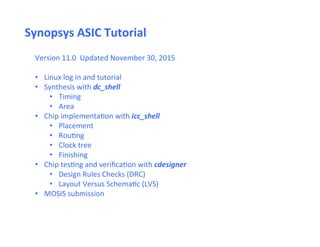
  • 1. Version  11.0    Updated  November  30,  2015   •  Linux  log  in  and  tutorial   •  Synthesis  with  dc_shell   •  Timing     •  Area   •  Chip  implementaEon  with  icc_shell   •  Placement   •  RouEng   •  Clock  tree   •  Finishing   •  Chip  tesEng  and  verificaEon  with  cdesigner     •  Design  Rules  Checks  (DRC)   •  Layout  Versus  SchemaEc  (LVS)   •  MOSIS  submission   Synopsys  ASIC  Tutorial  
  • 2. ssh  allows  us  to  login  to  the  system  and     “-­‐X”  enables  X  Windows  support   Quick  Linux  Tutorial   You  are  expected  to  have  a  working   knowledge  of  Linux  for  this  lab.     “pwd”  –  print  working  directory  –  should  be   your  user  directory   “cd”  –  change  directory  into   reference_design.       “ls  –alrt”  –  list  directory  contents.     Other  useful  Linux  commands:    man  –  help  for  commands      top    mkdir    passwd    cd  ~      cd  ..      rm    grep    more    cat     Type  xclock  and  you  should  see  a  clock   appear  if  X  Windows  is  working  properly    -­‐   shown  on  your  screen  but  running  remotely.   Log  in  with  Linux  
  • 3. cd  /opt/eda/synopsys/local/ON.PDK      (University  specific  –  ask  administrator)     cp      –r    reference_design/        ~/.   This  will  create  a  directory  structure.     cd  ~/reference_design     RTL  is  where  you  should  store  your  source  verilog  code.       SYN  is  where  you  will  perform  synthesis.      Update  the  script  “dc_good.tcl”  in  scripts   and  invoke  “dc_shell  –f  dc_good.tcl  |  tee  logs/output.syn”       PNR  is  where  you  will  perform  place  and  route.    Update  the  script  “icc_good.tcl”  in   scripts  and  invoke  “ic_shell  –f  icc_good.tcl  |  tee  logs/output.ic”     CUSTOM  is  where  you  store  reference  files.  Eg:  matlab  files  that  create  test  vectors   and  expected  results,  simulaEon  will  use  these  vectors  and  match  the  results.     SIM  is  where  you  store  your  simulaEon  files.    OpEonal  in  this  case.     GOLDEN  is  where  you  store  your  final  files  –  RTL,  GDS,  SDC,  TB.v,  and  scripts.   Copy  the  Reference  Design   logs/output.dc?  Or  outpu
  • 4. Simple  reference  design   Two  counters  –  one  clocked  by  external   clock,  the  other  by  an  internally   generated  clock.    All  clocks  have  to  be   idenEfied  for  staEc  Eming  to  work   correctly.      Total  of  40  flip-­‐flops  no   where  near  the  limit  in  terms  of  area   for  this  chip  size.     Only  four  outputs  and  two  inputs,   power  and  ground.    Total  is  8  pins.   Design  Compiler  -­‐  Reference  Design    
  • 5. cd  to  syn  directory  for  synthesis   cd  syn   Edit  and  update  the  script  “dc_good.tcl”  for  your  specific  design    idenEfy  file  and  module  name    idenEfy  clocks  and  frequency   source  /opt/eda/synopsys/synopsys.cshrc-­‐20151021  (university  specific  –  ask  admin)   Run  “dc_shell  –f  ”  to  invoke  script  as  shown  above  in  shell.   Look  in  reports  for  quality  of  output  by  reading  area  and  Eming  reports.     The  tool  can  be  opened  in  gui  format  as  well  –  “dc_shell  –gui”  although  synthesis  is   tradiEonally  done  with  a  script  only.   Design  Compiler  -­‐  Prepare  for  synthesis  
  • 6. Design  Compiler  -­‐  Checking  synthesis   During  synthesis  you  should  see  standard  output.     Flip-­‐flops  will  be  idenEfied.    Make  sure  this  make  sense.    I  have  two  20  bit   counters  in  the  reference  design  so  this  report  looks  reasonable.         Also  look  for  latches  which  indicates  a  problem  in  your  RTL.    All  if  statements   need  an  else  and  if  missing  can  cause  latches.  
  • 7. Aier  script  is  run,  look  for  return  values  of  1  for  all  lines.  0  is  a  failure  for  the  command.   In  results  you  will  have  a  *postsynth.v  as  your  netlist  and  a  sdc  file  with  Eming  info.   Check  the  netlist  to  make  sure  it  looks  reasonable.   In  logs,  you  will  see  the  commands  and  output.    Search  for  errors  and  “0’s”.   In  reports,  check  all  files  thoroughly.    Timing  –  check  that  criEcal  path  passes  and  is  legiEmate.    Area  –  not  too  big.    I  will  report  numbers  that  are  reasonable  in  class.    Power  is  interesEng  but  not  very  accurate.    Power  is  data  dependent  but  you  can      improve  by  adding  switching  data  from  the  simulator  VCS.   Design  Compiler  -­‐  AHer  synthesis   Final  Report:  Add  Lming  and   area  reports  to  final  report.  
  • 8. Design  Compiler  -­‐  Checking  synthesis   Top  of  the  netlist  should  have  your  module  name,  IO’s  and  nets.     You  will  see  some  starEng  with  a  back  slash  which  is  an  escape  character  as   some  tools  cannot  handle  square  brackets  and  this  character  is  used  to  escape.  
  • 9. Design  Compiler  -­‐  Checking  synthesis   Tri’s  will  be  inserted  due  to  the  IO’s  being  bidirecEonal.     Also,  look  at  the  gates.    DCX1  is  a  flip-­‐flop.    Scroll  down  to  check  all  of  the  gates.  
  • 10. Design  Compiler  -­‐  Checking  synthesis   Pad_bidirhe  are  the  IO  cells  and  you  should  see  other  gates  like  NAND2X1.     NAND2X1  is  the  smallest  2  input  NAND  gate.    X1  means  small  and  the  2  is  the   number  of  inputs.      A  and  B  are  in  and  Y  is  the  output  pins  normally.  
  • 11. Design  Compiler  -­‐  Timing  report   Worse  case  path  for  main  clock.     Through  the  adder  from  bit  0  to  bit  19   as  expected.    20  nS  to  complete  and   finished  in  8.34  nS  so  Eme  to  spare  –   which  means  posiEve  slack  of  11.27  nS.     Passed  and  made  sense.  Note  that   these  Emings  are  only  for  setup   calculaEons  and  no  holds  are   completed.    Since  the  clock  tree  is  not     in  place  (ideal  clock  tree  assumed)   there  is  no  clock  skew  which  is  required   for  hold  violaEons.     Final  Report:  Add  Lming   report  to  final  report.  
  • 12. Check  for  latches  (should  not  exist)  and  that  the  basic  numbers  are  reasonable.     For  the  MOSIS  chip,  I  expect  that  3-­‐5  Emes  this  area  is  possible,  so  500,000  square  microns   should  fit  in  the  allocated  space.   Design  Compiler  -­‐  Area  report   Final  Report:  Add  area   report  to  final  report.    
  • 13. IC  Compiler  -­‐  Place,  route,  Lming  and  checks   The  icc_good.tcl  script  will  go  into  the  synthesis  directory   to  obtain  the  netlist  and  sdc  file  (Eming).     Note  that  the  script  has  commented  lines  indicaEng   different  secEons  of  the  script  that  will  be  run  piecemeal.   The  command  “return”  will  stop  the  script  and  is  used  to   run  to  a  specific  locaEon.  
  • 14. IC  Compiler  –  First  return  –  Floor  Plan   Run  to  first  “return”  in  script  –  start_gui  to  invoke  viewer.     You  will  need  to  run  to  this  point  twice:  once  just  to  create  an  IO  file  and  a  second  Eme   using  the  IO  file  file  with  the  line  “source  is_pad.tcl”  uncommented.     Run  the  first  Eme  and  change  the  IO  file  name  of  a  newly  created  file:     cp  set_pad_apributes_on_cell_xtal_chip_with_io.tcl    is_pad.tcl     Check  that  the  file  has  all  IO  declared.           Uncomment  the  “source  is_pad.tcl”  line  in  the  script  and  run  again.  
  • 15. IC  Compiler  –  First  return  –  Floor  Plan  
  • 16. IC  Compiler  –  First  return  –  Floor  Plan   Use  the  ruler  to  check  sizes  of  the  die.    1500  microns  is  the  max  size  for  each  side.    
  • 17. IC  Compiler  –  First  return  –  Floor  Plan   Change  the  visibility  selecEons  to  see  different  layers.    Pins  and  Site  rows  to  see  metals  and   where  the  standard  cells  will  be  placed  later.       Note  that  all  unplaced  cells  are  to  the  right  –  out  of  bounds  for  now.     Final   Report:  Add   screen  shot   to  final   report.    
  • 18. IC  Compiler  Second  return  –  Power  and  IO  Fill  
  • 19. IC  Compiler  Second  return  –  Power  and  IO  Fill   Should  see  power  lines  at  all  three  levels  and  ring  with  verEcal  straps.    IO  Ring  is  complete   but  you  must  set  the  visual  seqngs  to  “Max  Quality”.    Change  levels  to  1  or  2  to  see  into   lower  hierarchical  levels.    May  need  to  change  color  of  poly  to  see  transistors.  
  • 20. IC  Compiler  Third  Return  –  Placement  of  Cells   Final   Report:  Add   screen  shot   to  final   report.    
  • 21. IC  Compiler  –  Fourth  Return  -­‐  Clock  Tree     Invoke  “Report  Clock  Tree”  
  • 22. IC  Compiler  –  Fourth  Return  -­‐  Clock  Tree    
  • 23. IC  Compiler  –  Fourth  Return  -­‐  Clock  Tree     SelecEng  main_clock   Final   Report:  Add   screen  shot   to  final   report.    
  • 24. IC  Compiler  –  Fourth  Return  -­‐  Clock  Tree     SelecEng  “secondary_clock”  –  Note  no  IO  included  in  this  internal  clock.  
  • 25. =======================  Clock  Tree  Summary  ========================   Clock                                Sinks          CTBuffers  ClkCells    Skew            LongestPath  TotalDRC      BufferArea   -­‐-­‐-­‐-­‐-­‐-­‐-­‐-­‐-­‐-­‐-­‐-­‐-­‐-­‐-­‐-­‐-­‐-­‐-­‐-­‐-­‐-­‐-­‐-­‐-­‐-­‐-­‐-­‐-­‐-­‐-­‐-­‐-­‐-­‐-­‐-­‐-­‐-­‐-­‐-­‐-­‐-­‐-­‐-­‐-­‐-­‐-­‐-­‐-­‐-­‐-­‐-­‐-­‐-­‐-­‐-­‐-­‐-­‐-­‐-­‐-­‐-­‐-­‐-­‐-­‐-­‐-­‐-­‐-­‐-­‐-­‐-­‐-­‐-­‐-­‐-­‐-­‐-­‐-­‐-­‐-­‐-­‐-­‐-­‐-­‐-­‐-­‐-­‐-­‐-­‐-­‐-­‐-­‐-­‐-­‐   main_clock                      39                12                14                0.0493        2.0112            0                      4536.0000   second_clock                  20                4                  4                  0.0311        0.9414            0                      2016.0000       Post  RouEng  (skew  increased  :/  ):       =======================  Clock  Tree  Summary  ========================   Clock                                Sinks          CTBuffers  ClkCells    Skew            LongestPath  TotalDRC      BufferArea   -­‐-­‐-­‐-­‐-­‐-­‐-­‐-­‐-­‐-­‐-­‐-­‐-­‐-­‐-­‐-­‐-­‐-­‐-­‐-­‐-­‐-­‐-­‐-­‐-­‐-­‐-­‐-­‐-­‐-­‐-­‐-­‐-­‐-­‐-­‐-­‐-­‐-­‐-­‐-­‐-­‐-­‐-­‐-­‐-­‐-­‐-­‐-­‐-­‐-­‐-­‐-­‐-­‐-­‐-­‐-­‐-­‐-­‐-­‐-­‐-­‐-­‐-­‐-­‐-­‐-­‐-­‐-­‐-­‐-­‐-­‐-­‐-­‐-­‐-­‐-­‐-­‐-­‐-­‐-­‐-­‐-­‐-­‐-­‐-­‐-­‐-­‐-­‐-­‐-­‐-­‐-­‐-­‐-­‐-­‐   main_clock                      39                12                14                0.1113        1.9813            0                      4536.0000   second_clock                  20                4                  4                  0.0319        0.9401            0                      2016.0000   1   IC  Compiler  –  Fourth  Return  -­‐  Clock  Tree     In  90nm  technology,  0.2  ns  of  skew  was  considered  acceptable.    Skew  isn’t  a  problem  if   you  pass  hold  Emings  though.   Final   Report:  Add   this  output   to  your  final   report.    
  • 26. IC  Compiler  –  Fourth  Return  -­‐  Clock  Tree     Check  Eming  report  in  log.    Need  “Met”  next  to  slack.  
  • 27. IC  Compiler  –  Fourth  Return  -­‐  Clock  Tree     Check  QoR  report  for  hold  violaEons  aier  the  tree.     Note  that  hold  violaEons  are  only  possible  aier  a   clock  tree  has  been  synthesized  as  clock  skew   causes  hold  violaEons.    Previous  Eming  reports  only   performed  setup  violaEons  checks.  
  • 28. IC  Compiler  –  FiHh  Return  -­‐  RouLng   Final   Report:  Add   screen  shot   to  final   report.    
  • 29. IC  Compiler  –  Well  filler  
  • 30. IC  Compiler  –  Metal  Density  Fill  
  • 31. verify_pg_nets       Checking  [gnd!]:                  There  are  no  floaEng  shapes                  All  the  pins  are  connected.                  No  errors  are  found.   Checking  [vdd!]:                  There  are  no  floaEng  shapes                  All  the  pins  are  connected.                  No  errors  are  found.   Checked  2  nets,  0  have  Errors   Update  error  cell  ...   1       verify_lvs       **  Total  FloaEng  ports  are  14.   **  Total  FloaEng  Nets  are  0.   **  Total  OPEN  Nets  are  0.   **  Total  Electrical  Equivalent  Error  are  0.   **  Total  Must  Joint  Error  are  0.       Check  floaEng  nets  are  on  unused   outputs  of  cells.    This  is  ok.     Check  the  reports  directory  for   Eming  and  QoR  reports  for  passing   all  Eming  checks  including  holds.   IC  Compiler  –  Final  Check  Off  
  • 32. IC  Compiler  –  Final  Check  Off  
  • 33. Check  floaEng  nets  are  on  unused   outputs  of  cells.    This  is  ok.   IC  Compiler  –  Final  Check  Off  
  • 34. Data_in  and  Data_inB  from  IO  must  float  if  they  are  output  pins.   IC  Compiler  –  Final  Check  Off  
  • 35. Custom  Designer  –  Import  GDS   Go  to  “custom”  directory  and  invoke  “cdesigner  &”,  create  a  library,  read   in  the  GDS,  add  metal  3  art  (opEonal)  and  run  final  DRCs.     We  will  be  performing  DRCs  on  the  logic  level  and  not  check  the  IO’s  as   these  are  known  to  be  good  and  have  false  problems  with  DRC  rules.     Before  you  run  the  DRCs  -­‐  you  can  use  “add  net”  aier  selecEng  “metal3”   and  add  metal  art  work  (e.g.  your  name,  a  diagram,  etc.)    
  • 36. Custom  Designer  –  Create  new  library   Create  “new  library”  to  “import  stream”  the  GDS  into  with  the  correct  technology.    
  • 37. Custom  Designer  –  Import  GDS   Import  “stream”  allows  us  to  read  in  the  GDS  file  created  by  IC  Compiler  and  later   to  be  sent  to  MOSIS  for  fabricaEon.    The  GDS  shows  all  geometries  of  the   fabricated  device.    
  • 38. Custom  Designer  –  File  -­‐>  Import  Stream   IC  Compiler  script  command:     “save_mw_cel  -­‐as  ${design_name}”    determines  the  Top  Cell.     IC  Compiler  script  command:   “write_stream  -­‐lib_name  MW_${design_name}_LIB  -­‐format  gds  results/${design_name}.gds   determines  the  file  name  of  the  GDS  filename.  
  • 39. Custom  Designer  –  Open  Layout  
  • 40. Custom  Designer  –  Draw  Images  in  Metal  3   f  –  fits  the  design  to  the  window.  
  • 41. Custom  Designer  –  Draw  Images  in  Metal  3   Shii  F  –  shows  all  lower  hierarchical  layers.    This  shows  chip  aier  shii  F.   Final   Report:  Add   screen  shot   to  final   report.    
  • 42. Custom  Designer  –  Draw  Images  in  Metal  3   On  the  right  you  can  select  metal  3  and  the  glasses  icon  to  only  see  Metal  3.   Control  R  –  redraws  aier  a  change.  
  • 43. Custom  Designer  –  Draw  Images  in  Metal  3   On  the  right  you  can  select  create  interconnect  and  draw  lines.    There  is  a  submenu   that  allows  you  to  change  thickness  and  permiped  angles.     Warning:  Sharp  acute  angles  and  insufficient  space  between  lines  can  cause  DRC   errors  later.      
  • 44. Custom  Designer  –  Run  DRCs   Before  we  can  run  checks,  we  must  flapen  the  design.      Open  Hierarchical  Navigator.    
  • 45. Custom  Designer  –  Run  DRCs   Select  flapen  from  edit  menu.  
  • 46. Custom  Designer  –  Run  DRCs   There  will  be  “flapen”  submenu  in  the  tool  bar  and  set  the  switches  according  to   the  picture  below.   With  the  mouse,  select  the  enEre  design  by   dragging  a  box  around  everything  including   IO’s.     Then  click  the  check  mark  on  the  far  right  of   the  menu.     You  should  see  only  one  instance  with  sub-­‐ instances  in  the  Hierarchical  Navigator  aier   you  click  on  the  refresh.  
  • 47. Custom  Designer  –  Run  DRCs   Use  the  verificaEon  menu  to  run  final  DRCs  regardless  of  whether  you  added  any   metal  paperns.    Only  select  the  internal  core  and  avoid  the  IO’s  as  there  is  an  issue   with  the  rules  for  the  cells  which  is  not  real  and  can  be  ignored.  
  • 48. Custom  Designer  –  Run  DRC   Fill  in  the  following  fields  of  the  DRC  setup  pane  –  “Main”.    The  runset  file  should   be  in  your  custom  directory.    Press  the  refresh  bupon  next  to  runset  field.    
  • 49. Custom  Designer  –  Run  DRC   If  you  press  the  refresh  bupon  in  the  Main  panel  next  to  the  runsets,  you  should   see  fields  in  this  “control  variable”  secEon.      There  are  none  in  this  picture  as   Hercules  (DRC  checker)  was  not  yet  installed.    
  • 50. Custom  Designer  –  Run  DRC   In  Custom  OpEons,  click  the  “select  window”  bupon  and  you  will  be  allowed  to   select  from  the  main  window  what  will  be  DRC  checked.    Since  there  are  problems   in  the  IO  that  are  not  real  DRCs  and  the  IO’s  are  proven,  we  are  only  going  to   check  the  interior  secEon  of  the  chip.    Select  the  interior  by  drawing  a  box  around   the  chip  but  avoiding  the  IO  rings.    Coordinates  will  show  in  the  field  and  should   be  similar  to  what  is  shown  here  –  approximately  250,  1250,  1250,  1250.     Select  Layer  Map  located  in   custom  directory   Now  click  OK  to  run  DRCs.    
  • 51. Custom  Designer  –  Example  failure   Metal  3  with  DRC  errors    
  • 52. Custom  Designer  –  Example  failure   Metal  3  DRC  errors  found  
  • 53. Custom  Designer  –  Example  failure   Select  errors  to  show  locaEon  of  error   Fix  error  and  run  DRC  checks  again  
  • 54. File  -­‐>  Export  -­‐>  Stream     Export  GDS  file  
  • 55. Stream  File  –  name  of  final  gds  file,  Library  –  GDS_in,  Top_cell  –  Name  of  your  top  cell   Export  GDS  file  
  • 56. Layer  Map  –  AMI06_UofU_layer_map_export     Export  GDS  file  
  • 57. For  fabricaEon  there  are  minimum  metal  densiEes.    The  script  below  checks  densiEes   for  each  metal  layer.   cd  ~/reference_design/custom/density_check   Update  cell  in  reportDensity.rs     Run  check_density  script  as  shown  below  in  shell.   Look  at  [Design_Name].LAYOUT_ERRORS  file  for  errors.                       Metal  Density  Check  
  • 58. The  required  density  for  each  layer  is  shown  below.   Poly  between  .12  -­‐  .3   Metal  1  between  .3  -­‐  .8   Metal  2  between  .3  -­‐  .8   Metal  3  between  .3  -­‐  .8   Metal  Density  Check  
  • 59. MOSIS  Submission  Tutorial  for    ON  Semiconductor  0.5u  C5F  CMOS    
  • 61. Overview   Aier  being  assigned  a  design  name,  number  and  password  go  to:     www.mosis.com       Select  “fabricate  request”  and  fill  in  the  form  for  the  secure  hpps  upload  opEon     Put your five digit number and password here.
  • 62. Use your design number Run the crc program on your gds for these two numbers
  • 63. Use your email address, phone number and design.
  • 64. Put any information that will make receiving the chips easier