1. • III-V nitride-based components are more radiation resistant than their silicon
counterparts.
• Using more durable components potentially require less shielding; leading to
lighter, more efficient missions.
• Light emitting diodes (LEDs) will be characterized by their peak wavelength as
detected by a photodiode array.
• Experiment is part of Simulation-to-Flight 1 (STF-1) mission.
• Built LED mesas in-house at the WVU Shared Research Facilities.
• LEDs are tuned to emit at a peak wavelength of 465 nm.
• First circuit contains a Low-power Optoelectronic Characterizer for CubeSat
(LOCC) which will measure the current drawn from the LEDs.
• Second circuit contains the electroluminescence module, which will measure
the tristimulus values emitted from the LEDs.
• MTCSiCF color sensor and MCDC04 ADC output the XYZ tristimulus values.
3U CubeSat for the STF-1
Mission
LED Structure
(Left) Both LED and PD have coating (Middle) Only
PD has coating (Right) No coating.
LEDs
• The electroluminescence of an
LED is limited by the light able
to escape the protective shell
surrounding the structure.
• Limiting the epoxy protecting the
LEDs from radiation can achieve
greater output.
Color Science
• Used the CIE 1931 color spaces.
• (x.y) coordinates for the
chromaticity diagram can be
calculated from the tristimulus
XYZ values.
• Dominant wavelength is
determined by extrapolating a line
going through the white light
reference point and sensor value to
the edge of the locus.
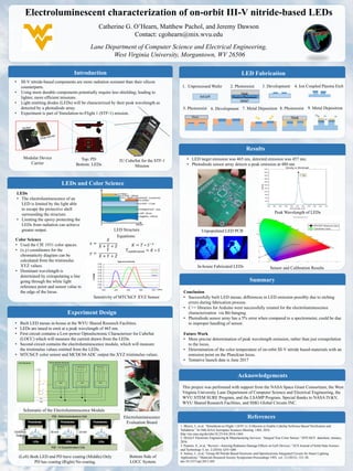
Electroluminescent characterization of on-orbit III-V nitride-based LEDs
Catherine G. O’Hearn, Matthew Pachol, and Jeremy Dawson
Contact: cgohearn@mix.wvu.edu
Lane Department of Computer Science and Electrical Engineering,
West Virginia University, Morgantown, WV 26506
Electroluminescence
Evaluation Board
Sensor and Colorimeter Results
Modular Device
Carrier
Top: PD
Bottom: LEDs
Equations:
𝑥 =
𝑋
𝑋 + 𝑌 + 𝑍
𝑦 =
𝑌
𝑋 + 𝑌 + 𝑍
𝐾 = 𝑇 ∗ 𝑆−1
𝑇𝑐𝑎𝑙𝑖𝑏𝑟𝑎𝑡𝑒𝑑 = 𝐾 ∗ 𝑆
This project was performed with support from the NASA Space Grant Consortium, the West
Virginia University Lane Department of Computer Science and Electrical Engineering, the
WVU STEM SURE Program, and the LSAMP Program. Special thanks to NASA IV&V,
WVU Shared Research Facilities, and SMG Global Circuits INC.
1. Morris, J., et al. “Simulation-to-Flight 1 (STF-1): A Mission to Enable CubeSat Software-Based Verification and
Validation.” In 54th AIAAAerospace Sciences Meeting, 1464, 2016.
http://arc.aiaa.org/doi/abs/10.2514/6.2016-1464.
2. MAZeT Electronic Engineering & Manufacturing Services. “Integral True Color Sensor.” MTCSiCF datasheet, January,
2016.
3. Pearton, S., et al, “Review—Ionizing Radiation Damage Effects on GaN Devices.” ECS Journal of Solid State Science
and Technology 5, no. 2 (2016): Q35–Q60
4. Justice, J., et al, “Group III-Nitride Based Electronic and Optoelectronic Integrated Circuits for Smart Lighting
Applications.” Materials Research Society Symposium Proceedings 1492, vol. 12 (2012): 123–28.
doi:10.1557/opl.2013.369.
Conclusion
• Successfully built LED mesas; differences in LED emission possibly due to etching
errors during fabrication process.
• C++ libraries for Arduino were successfully created for the electroluminescence
characterization via Bit-banging
• Photodiode sensor array has a 5% error when compared to a spectrometer, could be due
to improper handling of sensor.
Future Work
• More precise determination of peak wavelength emission, rather than just extrapolation
to the locus.
• Determination of the color temperature of on-orbit III-V nitride based-materials with an
emission point on the Planckian locus.
• Tentative launch date is June 2017
Bottom Side of
LOCC System
Sensitivity of MTCSiCF XYZ Sensor
Introduction
LEDs and Color Science
Summary
Acknowledgements
Experiment Design
References
Schematic of the Electroluminescence Module
In-house Fabricated LEDs
• LED target emission was 465 nm, detected emission was 457 nm.
• Photodiode sensor array detects a peak emission at 480 nm
Peak Wavelength of LEDs
Unpopulated LED PCB
Results
LED Fabrication
1. Unprocessed Wafer
InGaN
2. Photoresist 3. Development
5. Photoresist 6. Development 7. Metal Deposition 8. Photoresist
4. Ion Coupled Plasma Etch
9. Metal Deposition
Sensor and Calibration Results