
Recommended
Recommended
More Related Content
Similar to ISP1807 : Full BLE 5.0
Similar to ISP1807 : Full BLE 5.0 (20)
More from Anne Stiegler
More from Anne Stiegler (20)
Recently uploaded
Recently uploaded (20)
ISP1807 : Full BLE 5.0
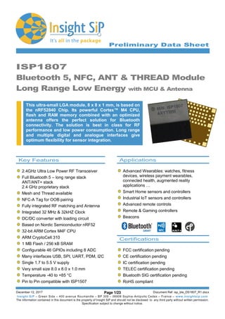
- 1. Preliminary Data Sheet December 12, 2017 Page 1/23 Document Ref: isp_ble_DS1807_R1.docx Insight SiP – Green Side – 400 avenue Roumanille – BP 309 – 06906 Sophia-Antipolis Cedex – France – www.insightsip.com The information contained in this document is the property of Insight SiP and should not be disclosed to any third party without written permission. Specification subject to change without notice. ISP1807 Bluetooth 5, NFC, ANT & THREAD Module Long Range Low Energy with MCU & Antenna This ultra-small LGA module, 8 x 8 x 1 mm, is based on the nRF52840 Chip. Its powerful Cortex™ M4 CPU, flash and RAM memory combined with an optimized antenna offers the perfect solution for Bluetooth connectivity. The solution is best in class for RF performance and low power consumption. Long range and multiple digital and analogue interfaces give optimum flexibility for sensor integration. Applications Advanced Wearables: watches, fitness devices, wireless payment wearables, connected health, augmented reality applications … Smart Home sensors and controllers Industrial IoT sensors and controllers Advanced remote controls Remote & Gaming controllers Beacons Certifications FCC certification pending CE certification pending IC certification pending TELEC certification pending Bluetooth SIG certification pending RoHS compliant Key Features 2.4GHz Ultra Low Power RF Transceiver Full Bluetooth 5 – long range stack ANT/ANT+ stack 2.4 GHz proprietary stack Mesh and Thread available NFC-A Tag for OOB pairing Fully integrated RF matching and Antenna Integrated 32 MHz & 32kHZ Clock DC/DC converter with loading circuit Based on Nordic Semiconductor nRF52 32-bit ARM Cortex M4F CPU ARM CryptoCell 310 1 MB Flash / 256 kB SRAM Configurable 46 GPIOs including 8 ADC Many interfaces USB, SPI, UART, PDM, I2C Single 1.7 to 5.5 V supply Very small size 8.0 x 8.0 x 1.0 mm Temperature -40 to +85 °C Pin to Pin compatible with ISP1507
- 2. Preliminary Data Sheet December 12, 2017 Page 2/23 Document Ref: isp_ble_DS1807_R1.docx Insight SiP – Green Side – 400 avenue Roumanille – BP 309 – 06906 Sophia-Antipolis Cedex – France – www.insightsip.com The information contained in this document is the property of Insight SiP and should not be disclosed to any third party without written permission. Specification subject to change without notice. BLE MODULE ISP1807 Contents 1. Block Diagram .......................................................................................................................................................3 2. Specifications ........................................................................................................................................................4 2.1. Important Notice.........................................................................................................................................4 2.2. Absolute Maximum Ratings ........................................................................................................................4 2.3. Operating Conditions..................................................................................................................................4 2.4. Power Consumption ...................................................................................................................................5 2.5. Clock Sources............................................................................................................................................5 2.6. Radio Specifications...................................................................................................................................5 2.7. Electrical Schematic ...................................................................................................................................8 3. Pin Description ......................................................................................................................................................9 4. Mechanical Outlines............................................................................................................................................12 4.1. Mechanical Dimensions............................................................................................................................12 4.2. SMT Assembly Guidelines........................................................................................................................13 4.3. Antenna Keep-Out Zone...........................................................................................................................13 5. Product Development Tools...............................................................................................................................14 5.1. Hardware .................................................................................................................................................14 5.2. Firmware..................................................................................................................................................14 5.3. Development Tools...................................................................................................................................15 6. Packaging & Ordering information....................................................................................................................16 6.1. Marking....................................................................................................................................................16 6.2. Prototype Packaging ................................................................................................................................16 6.3. Jedec Trays..............................................................................................................................................16 6.4. Tape and Reel..........................................................................................................................................17 6.5. Ordering Information.................................................................................................................................18 7. Storage & Soldering information.......................................................................................................................19 7.1. Storage and Handling...............................................................................................................................19 7.2. Moisture Sensitivity...................................................................................................................................19 7.3. Soldering information................................................................................................................................20 8. Quality & User information.................................................................................................................................21 8.1. Certifications ............................................................................................................................................21 8.2. USA – User information............................................................................................................................21 8.3. Canada – User information.......................................................................................................................21 8.4. RF Exposure Information..........................................................................................................................22 8.5. Informations concernant l'exposition aux fréquences radio (RF)................................................................22 8.6. Discontinuity.............................................................................................................................................22 8.7. Disclaimer ................................................................................................................................................23
- 3. Preliminary Data Sheet December 12, 2017 Page 3/23 Document Ref: isp_ble_DS1807_R1.docx Insight SiP – Green Side – 400 avenue Roumanille – BP 309 – 06906 Sophia-Antipolis Cedex – France – www.insightsip.com The information contained in this document is the property of Insight SiP and should not be disclosed to any third party without written permission. Specification subject to change without notice. BLE MODULE ISP1807 1. Block Diagram This module is based on nRF52840 Nordic Semiconductor 2.4GHz wireless System on Chip (SoC) integrating a 2.4 GHz transceiver, a 32-bit ARM Cortex™-M4F CPU, a 1 MB flash memory, a 256 kB RAM and analog and digital peripherals. It can support BLE, ANT/ANT+ and a range of proprietary 2.4 GHz protocols, such as Gazell from Nordic Semiconductor. Fully qualified BLE stacks for nRF52840 are implemented in the S140 SoftDevices which can be freely downloaded. ISP1807 can then be used in Bluetooth Central, Peripheral, Observer or Broadcaster role with up to 20 connections and for both ends of other proprietary protocols. nRF52840 platform also provides extensive software support for ANT and THREAD applications. Ultra-low power consumption and advanced power management enables battery lifetimes up to several years on a coin cell battery. Even though its very small size 8 x 8 x 1.0 mm, the module integrates decoupling capacitors, 32 MHz and 32.768 kHz crystals, load capacitors, DC-DC converter, RF matching circuit and antenna in addition to the wireless SoC. Only the addition of a suitable DC power source is necessary for BLE / ANT / THREAD connectivity. Sensor applications require the further addition of appropriate sensors. The antenna was designed to be optimized with several standard ground plane sizes. The NFC tag antenna can be connected externally.
- 4. Preliminary Data Sheet December 12, 2017 Page 4/23 Document Ref: isp_ble_DS1807_R1.docx Insight SiP – Green Side – 400 avenue Roumanille – BP 309 – 06906 Sophia-Antipolis Cedex – France – www.insightsip.com The information contained in this document is the property of Insight SiP and should not be disclosed to any third party without written permission. Specification subject to change without notice. BLE MODULE ISP1807 2. Specifications 2.1. Important Notice The electrical specifications of the module are directly related to the Nordic Semiconductor specifications for the nRF52840 chipset. Bellow information is only a summary of the main parameters. For more detailed information, especially about current consumption, please refer to the up-to-date specification of the chipset available on Nordic Semi website. 2.2. Absolute Maximum Ratings Parameter Min Typ Max Unit Main Supply Voltage respect to ground – VCC -0.3 3.9 V High Supply Voltage respect to ground – VCCH -0.3 5.8 V USB Supply Voltage respect to ground – VUSB -0.3 5.8 V IO Pin Voltage -0.3 3.9 V RF Input Level 10 dBm NFC Antenna pin current 80 mA Storage Temperature -40 +125 °C Moisture Sensitivity Level 5 - ESD Human Body Model 4000 V ESD Charged Device Model 750 V Flash Endurance 10000 cycles ATTENTION CONSERVE PRECAUTION FOR HANDLING ELECTROSTATIC SENSITIVE DEVICES Human Body Model Class 3A 2.3. Operating Conditions Parameter Min Typ Max Unit VCC Supply Voltage, independent of DCDC enable 1.75 3.0 3.6 V VCCH Supply Voltage, independent of DCDC enable 2.5 3.7 5.5 V VUSB Supply Voltage 4.35 5.0 5.5 V Extended Industrial Operating Temperature Range -40 +25 +85 °C
- 5. Preliminary Data Sheet December 12, 2017 Page 5/23 Document Ref: isp_ble_DS1807_R1.docx Insight SiP – Green Side – 400 avenue Roumanille – BP 309 – 06906 Sophia-Antipolis Cedex – France – www.insightsip.com The information contained in this document is the property of Insight SiP and should not be disclosed to any third party without written permission. Specification subject to change without notice. BLE MODULE ISP1807 2.4. Power Consumption Parameter Min Typ Max Unit Peak Current, Transmitter +8 dBm, VCC 3V + DCDC 14.1 mA Peak Current, Transmitter 0 dBm, VCC 3V + DCDC 4.9 mA Peak Current, Transmitter 0 dBm, VCCH 5V + DCDC 6.0 mA Peak Current, Receiver 1 Mbps, VCC 3V + DCDC 4.8 mA Peak Current, Receiver 2 Mbps, VCC 3V + DCDC 5.4 mA System OFF, no RAM retention 0.4 µA System ON, no RAM retention, wake on RTC 1.3 µA Additional RAM retention current per 4 KB block 30 N nA 2.5. Clock Sources Parameter Min Typ Max Unit Internal High Frequency Clock for RF Stability: 32 MHz Crystal Frequency Tolerance (1) +/- 40 ppm Internal Low Frequency Clock for BLE Synchronization: 32.768 kHz Crystal Frequency Tolerance (1) +/- 40 ppm Internal Low Frequency Clock for BLE Synchronization: RC Oscillator (2) +/- 250 ppm RF Frequency Tolerance for BLE Operation +/- 40 ppm (1) including initial tolerance, drift, aging, and frequency pulling (2) Frequency tolerance after calibration 2.6. Radio Specifications Parameter Min Typ Max Unit Frequency Range 2360 2500 Mhz Maximum Output Power 8 dBm Rx Sensitivity Level, BLE 1 Mbps -95 dBm Rx Sensitivity Level, BLE Long Range 125 kbps -103 dBm Antenna Gain 0.6 dBi EIRP -19.4 8.6 dBm Range Open field @1m height 100 M Data Rate 125 2000 kbps
- 6. Preliminary Data Sheet December 12, 2017 Page 6/23 Document Ref: isp_ble_DS1807_R1.docx Insight SiP – Green Side – 400 avenue Roumanille – BP 309 – 06906 Sophia-Antipolis Cedex – France – www.insightsip.com The information contained in this document is the property of Insight SiP and should not be disclosed to any third party without written permission. Specification subject to change without notice. BLE MODULE ISP1807 Typical Antenna Return Loss Module mounted on a USB dongle ground plane Radiation Pattern in 3 planes Module mounted on a USB dongle ground plane Gain measurement in dBi @ 2.45 GHz.
- 7. Preliminary Data Sheet December 12, 2017 Page 7/23 Document Ref: isp_ble_DS1807_R1.docx Insight SiP – Green Side – 400 avenue Roumanille – BP 309 – 06906 Sophia-Antipolis Cedex – France – www.insightsip.com The information contained in this document is the property of Insight SiP and should not be disclosed to any third party without written permission. Specification subject to change without notice. BLE MODULE ISP1807 Ground Plane Effect Simulation USB dongle ground plane (size : 18 x 30 mm²) Cell phone config 1 ground plane (size : 40 x 100 mm²) Cell phone config 1 with side ground plane (size : 40 x 100 mm²) Cell phone config 2 with side ground plane (size : 40 x 100 mm²) Cell phone config 3 with side ground plane (size : 40 x 100 mm²)
- 8. Preliminary Data Sheet December 12, 2017 Page 8/23 Document Ref: isp_ble_DS1807_R1.docx Insight SiP – Green Side – 400 avenue Roumanille – BP 309 – 06906 Sophia-Antipolis Cedex – France – www.insightsip.com The information contained in this document is the property of Insight SiP and should not be disclosed to any third party without written permission. Specification subject to change without notice. BLE MODULE ISP1807 2.7. Electrical Schematic Electrical schematic showing ISP1807 module connections
- 9. Preliminary Data Sheet December 12, 2017 Page 9/23 Document Ref: isp_ble_DS1807_R1.docx Insight SiP – Green Side – 400 avenue Roumanille – BP 309 – 06906 Sophia-Antipolis Cedex – France – www.insightsip.com The information contained in this document is the property of Insight SiP and should not be disclosed to any third party without written permission. Specification subject to change without notice. BLE MODULE ISP1807 3. Pin Description The module uses an LGA format with a double row of pads on a 0.65 mm pitch. The pad layout follows the QFN Jedec standard for 2 row LGA parts. The NC pads are to be connected to isolated metal pads on the application PCB for mechanical stability and reliability (drop test). Pin Name Pin function Description 1 VSS Ground Should be connected to ground plane on application PCB 2 P0_09 NFC1 Digital I/O NFC Input General purpose I/O pin NFC antenna connection 3 P0_12 TRACEDATA1 Digital I/O General purpose I/O pin Trace port output 4 P0_10 NFC2 Digital I/O NFC Input General purpose I/O pin NFC antenna connection 5 P0_14 Digital I/O General purpose I/O pin 6 P0_26 Digital I/O General purpose I/O pin 7 VSS Ground Should be connected to ground plane on application PCB 8 D+ Ground Should be connected to ground plane on application PCB 9 P0_16 Digital I/O General purpose I/O pin 10 D- Ground Should be connected to ground plane on application PCB 11 P0_21 Digital I/O General purpose I/O pin 12 VUSB Ground Should be connected to ground plane on application PCB 13 P0_18 RESET Digital I/O General purpose I/O pin Configurable as system RESET pin 14 VSS Ground Should be connected to ground plane on application PCB 15 P0_20 Digital I/O General purpose I/O pin 16 VSS Ground Should be connected to ground plane on application PCB 17 P0_22 Digital I/O General purpose I/O pin 18 VSS Ground Should be connected to ground plane on application PCB 19 P0_24 Digital I/O General purpose I/O pin 20 OUT_ANT Antenna I/O This pin is connected to the internal antenna It should be connected to Pin 22 OUT_MOD for normal operation 21 VSS Ground Should be connected to ground plane on application PCB 22 OUT_MOD Antenna I/O This pin is the RF I/O pin of the BLE module It should be connected to Pin 20 OUT_ANT for normal operation 23 VSS Ground Should be connected to ground plane on application PCB 24 VSS Ground Should be connected to ground plane on application PCB 25 VSS Ground Should be connected to ground plane on application PCB 26 VCC Power Power supply (1.7 – 3.6V) 27 P0_17 Digital I/O General purpose I/O pin 28 SWDIO Digital I/O Serial Wire Debug I/O for debug and programming 29 P0_13 Digital I/O General purpose I/O pin 30 SWDCLK Digital Input Serial Wire Debug clock input for debug and programming 31 VSS Ground Should be connected to ground plane on application PCB 32 P0_08 Digital I/O General purpose I/O pin 33 P0_07 TRACECLK Digital I/O General purpose I/O pin Trace port clock output
- 10. Preliminary Data Sheet December 12, 2017 Page 10/23 Document Ref: isp_ble_DS1807_R1.docx Insight SiP – Green Side – 400 avenue Roumanille – BP 309 – 06906 Sophia-Antipolis Cedex – France – www.insightsip.com The information contained in this document is the property of Insight SiP and should not be disclosed to any third party without written permission. Specification subject to change without notice. BLE MODULE ISP1807 Pin Name Pin function Description 34 P0_06 Digital I/O General purpose I/O pin 35 P0_04 AIN2 Digital I/O Analog Input General purpose I/O pin SAADC/COMP/LPCOMP input 36 P0_05 AIN3 Digital I/O Analog Input General purpose I/O pin SAADC/COMP/LPCOMP input 37 P0_15 Digital I/O General purpose I/O pin 38 P0_03 AIN1 Digital I/O Analog Input General purpose I/O pin SAADC/COMP/LPCOMP input 39 P0_27 Digital I/O General purpose I/O pin 40 P0_02 AIN0 Digital I/O Analog Input General purpose I/O pin SAADC/COMP/LPCOMP input 41 P0_25 Digital I/O General purpose I/O pin 42 P0_31 AIN7 Digital I/O Analog Input General purpose I/O pin SAADC/COMP/LPCOMP input 43 P0_11 TRACEDATA2 Digital I/O General purpose I/O pin Trace port output 44 P0_30 AIN6 Digital I/O Analog Input General purpose I/O pin SAADC/COMP/LPCOMP input 45 P0_19 Digital I/O General purpose I/O pin 46 P0_29 AIN5 Digital I/O Analog Input General purpose I/O pin SAADC/COMP/LPCOMP input 47 P0_23 Digital I/O General purpose I/O pin 48 P0_28 AIN4 Digital I/O Analog Input General purpose I/O pin SAADC/COMP/LPCOMP input 49 P1_02 Digital I/O General purpose I/O pin 50 P1_06 Digital I/O General purpose I/O pin 51 P1_15 Digital I/O General purpose I/O pin 52 P1_14 Digital I/O General purpose I/O pin 53 P1_13 Digital I/O General purpose I/O pin 54 P1_05 Digital I/O General purpose I/O pin 55 P1_08 Digital I/O General purpose I/O pin 56 P1_09 TRACEDATA3 Digital I/O General purpose I/O pin Trace port output 57 P1_00 TRACEDATA0 Digital I/O General purpose I/O pin Trace port output 58 P1_03 Digital I/O General purpose I/O pin 59 P1_12 Digital I/O General purpose I/O pin 60 P1_10 Digital I/O General purpose I/O pin 61 P1_11 Digital I/O General purpose I/O pin 62 P1_07 Digital I/O General purpose I/O pin 63 P1_04 Digital I/O General purpose I/O pin 64 P1_01 Digital I/O General purpose I/O pin 65 to 78 NC Not Connected Isolated pad on application PCB for mechanical stability
- 11. Preliminary Data Sheet December 12, 2017 Page 11/23 Document Ref: isp_ble_DS1807_R1.docx Insight SiP – Green Side – 400 avenue Roumanille – BP 309 – 06906 Sophia-Antipolis Cedex – France – www.insightsip.com The information contained in this document is the property of Insight SiP and should not be disclosed to any third party without written permission. Specification subject to change without notice. BLE MODULE ISP1807 ISP1807 pad placement and pin assignment for the LGA QFN package TOP VIEW
- 12. Preliminary Data Sheet December 12, 2017 Page 12/23 Document Ref: isp_ble_DS1807_R1.docx Insight SiP – Green Side – 400 avenue Roumanille – BP 309 – 06906 Sophia-Antipolis Cedex – France – www.insightsip.com The information contained in this document is the property of Insight SiP and should not be disclosed to any third party without written permission. Specification subject to change without notice. BLE MODULE ISP1807 4. Mechanical Outlines 4.1. Mechanical Dimensions Dimensional drawing for 8 x 8 x 1 mm, 62-Pad LGA Package
- 13. Preliminary Data Sheet December 12, 2017 Page 13/23 Document Ref: isp_ble_DS1807_R1.docx Insight SiP – Green Side – 400 avenue Roumanille – BP 309 – 06906 Sophia-Antipolis Cedex – France – www.insightsip.com The information contained in this document is the property of Insight SiP and should not be disclosed to any third party without written permission. Specification subject to change without notice. BLE MODULE ISP1807 4.2. SMT Assembly Guidelines For PCB Land Patterns and Solder Mask layout, Insight SiP recommends to use the same dimensions as module pads, ie 0.4 x 0.4 mm for standard pads and 0.8 x 0.8 mm for corner pads. Please contact Insight SiP for more detailed information. 4.3. Antenna Keep-Out Zone For optimal antenna performance, it is recommended to respect a metal exclusion zone to the edge of the board: no metal, no traces and no components on any application PCB layer except mechanical LGA pads.
- 14. Preliminary Data Sheet December 12, 2017 Page 14/23 Document Ref: isp_ble_DS1807_R1.docx Insight SiP – Green Side – 400 avenue Roumanille – BP 309 – 06906 Sophia-Antipolis Cedex – France – www.insightsip.com The information contained in this document is the property of Insight SiP and should not be disclosed to any third party without written permission. Specification subject to change without notice. BLE MODULE ISP1807 5. Product Development Tools 5.1. Hardware In order to assist clients in developing their Bluetooth Smart solutions based on the ISP1807, Insight SIP offers a Development Kit containing: - One Interface Board - J-Link Lite CortexM-9 JTAG/SWD Emulator - One Test Board - A Development Dongle - 5 ISP1807 module samples - Cables, power supply and coin battery holder Using this development kit, product developers can use a working solution as starting point to develop their own products. Time to market is saved by avoiding starting from a blank sheet of paper. In addition, there may be some applications that use the hardware as is. Please refer to the documentation for more information: http://www.insightsip.com/fichiers_insightsip/pdf/ble/ISP1807/isp_ble_DS1807_DK.pdf 5.2. Firmware 1807 supports Bluetooth Low Energy protocol stacks, ANT protocol stacks as well as 2.4 GHz protocol stacks, including Gazell. All are available as downloads at www.nordicsemi.com. The S140 SoftDevice is a Bluetooth® low energy (BLE) Central and Peripheral protocol stack solution supporting up to three Central and one Peripheral simultaneous connections and concurrent Observer and Broadcaster roles. It integrates a low energy Controller and Host, and provides a full and flexible API for building Bluetooth low energy System on Chip (SoC) solutions.
- 15. Preliminary Data Sheet December 12, 2017 Page 15/23 Document Ref: isp_ble_DS1807_R1.docx Insight SiP – Green Side – 400 avenue Roumanille – BP 309 – 06906 Sophia-Antipolis Cedex – France – www.insightsip.com The information contained in this document is the property of Insight SiP and should not be disclosed to any third party without written permission. Specification subject to change without notice. BLE MODULE ISP1807 5.3. Development Tools The following development tools and software are recommended for using and testing ISP1807 module: Nordic Semiconductor nRFgo Studio: Downloadable after registering at www.nordicsemi.com. Nordic Semiconductor Master Control Panel: Downloadable after registering at www.nordicsemi.com. Keil MDK-ARM Lite: Downloadable from https://www.keil.com/demo/eval/arm.htm. Segger J-Link Lite: Downloadable from http://www.segger.com/jlink-software.html. nRF52 Software Development Kit (SDK): nRF52 SDK can be downloaded after registering at www.nordicsemi.com. It contains example of source codes applications (C language): - Precompiled HEX files - Source code - Keil ARM project files - IAR project files
- 16. Preliminary Data Sheet December 12, 2017 Page 16/23 Document Ref: isp_ble_DS1807_R1.docx Insight SiP – Green Side – 400 avenue Roumanille – BP 309 – 06906 Sophia-Antipolis Cedex – France – www.insightsip.com The information contained in this document is the property of Insight SiP and should not be disclosed to any third party without written permission. Specification subject to change without notice. BLE MODULE ISP1807 6. Packaging & Ordering information 6.1. Marking ISP1807 Part Number TT 2 letters Module Type (see section 6.5) YY 2 digits year number WW 2 digits week number R 1 letter Hardware revision 6.2. Prototype Packaging For engineering samples and prototype quantities up to 99 units, deliveries are provided in thermoformed trays or cut tapes. Please order with “ST” code packaging suffix. These parts must be backed prior to assembly (see section 7.2). CAUTION MOISTURE SENSITIVE DEVICES 6.3. Jedec Trays For pre-production volumes, ISP1807 are available in Jedec trays. They are delivered in sealed pack with desiccant pack and humidity sensors. These Jedec trays are also suitable for further baking. Please see section 7.2 for more information on moisture sensitivity. Please order with “JT” code packaging suffix. Refer to tray sizes below. Complete information on Jedec trays is available on request. M /N : I S P 1 8 0 7 T T Y Y W W R LEVEL 5
- 17. Preliminary Data Sheet December 12, 2017 Page 17/23 Document Ref: isp_ble_DS1807_R1.docx Insight SiP – Green Side – 400 avenue Roumanille – BP 309 – 06906 Sophia-Antipolis Cedex – France – www.insightsip.com The information contained in this document is the property of Insight SiP and should not be disclosed to any third party without written permission. Specification subject to change without notice. BLE MODULE ISP1807 6.4. Tape and Reel ISP1807 are also available in Tape & Reel. They are delivered in sealed pack with desiccant pack and humidity sensors. Reels are proposed in standard quantities of 500 units (180mm / 7” reel) or 2000 units (330mm / 13” reel) only. Please order with “RS” code packaging suffix for 500-unit reels and “R2” for 2000-unit reels.
- 18. Preliminary Data Sheet December 12, 2017 Page 18/23 Document Ref: isp_ble_DS1807_R1.docx Insight SiP – Green Side – 400 avenue Roumanille – BP 309 – 06906 Sophia-Antipolis Cedex – France – www.insightsip.com The information contained in this document is the property of Insight SiP and should not be disclosed to any third party without written permission. Specification subject to change without notice. BLE MODULE ISP1807 6.5. Ordering Information I S P 1 8 0 7 - T T - Z Z ▼ ▼ ▼ ▼ ▼ ▼ ▼ ▼ ▼ ▼ ▼ ▼ I S P 1 8 0 7 Part Number - A BLE / ANT / THREAD protocol type - G 1 MB Flash / 256 kB RAM memory type - D K Development kit (1) - T B Test board (1) - S T Unsealed Tray or Cut Tape - J T Jedec Tray Packaging - R S Reel of 500 units - R 2 Reel of 2000 units (1) Please see section 5.1 and refer to the following documentation for more information on development kit and test board: http://www.insightsip.com/fichiers_insightsip/pdf/ble/ISP1807/isp_ble_DS1807_DK.pdf http://www.insightsip.com/fichiers_insightsip/pdf/ble/ISP1807/isp_ble_ANXXXXX.pdf
- 19. Preliminary Data Sheet December 12, 2017 Page 19/23 Document Ref: isp_ble_DS1807_R1.docx Insight SiP – Green Side – 400 avenue Roumanille – BP 309 – 06906 Sophia-Antipolis Cedex – France – www.insightsip.com The information contained in this document is the property of Insight SiP and should not be disclosed to any third party without written permission. Specification subject to change without notice. BLE MODULE ISP1807 7. Storage & Soldering information 7.1. Storage and Handling Keep this product away from other high frequency devices which may interfere with operation such as other transmitters and devices generating high frequencies. Do not expose the module to the following conditions: - Corrosive gasses such as Cl2, H2S, NH3, SO2, or NOX - Extreme humidity or salty air - Prolonged exposure to direct Sunlight - Temperatures beyond those specified for storage Do not apply mechanical stress Do not drop or shock the module Avoid static electricity, ESD and high voltage as these may damage the module ATTENTION CONSERVE PRECAUTION FOR HANDLING ELECTROSTATIC SENSITIVE DEVICES 7.2. Moisture Sensitivity All plastic packages absorb moisture. During typical solder reflow operations when SMDs are mounted onto a PCB, the entire PCB and device population are exposed to a rapid change in ambient temperature. Any absorbed moisture is quickly turned into superheated steam. This sudden change in vapor pressure can cause the package to swell. If the pressure exerted exceeds the flexural strength of the plastic mold compound, then it is possible to crack the package. Even if the package does not crack, interfacial delamination can occur. Since the device package is sensitive to moisture absorption, it is recommended to bake the product before assembly. The baking process for dry packing is 24 hours at 125°C. ISP1807 has been tested MSL-5 according to standards. After baking, modules can be exposed to ambient room conditions (approximately 30 °C/60%RH) during 48 hours before assembly on the PCB. CAUTION MOISTURE SENSITIVE DEVICES LEVEL 5
- 20. Preliminary Data Sheet December 12, 2017 Page 20/23 Document Ref: isp_ble_DS1807_R1.docx Insight SiP – Green Side – 400 avenue Roumanille – BP 309 – 06906 Sophia-Antipolis Cedex – France – www.insightsip.com The information contained in this document is the property of Insight SiP and should not be disclosed to any third party without written permission. Specification subject to change without notice. BLE MODULE ISP1807 7.3. Soldering information Recommendation for RoHS reflow process is according to Jedec J–STD-020 and 033 standard profiles. Preheat/Soak Temperature Min (Tsmin) Temperature Max (Tsmax) Time (ts) from (Tsmin to Tsmax) 150 °C 200 °C 60-120 sec Peak package body temperature (Tp) 260°C (+0/-5°C) Classification Temperature (Tc) Time (tp) maintained above TC-5 °C 260 °C 30 sec Ramp-up rate (TL to Tp) 3 °C/sec max Ramp-down rate (Tp to TL) 6 °C/sec max Liquidous temperature (TL) Time (tL) maintained above TL 217 °C 60-150 sec Time 25 °C to peak temperature 8 mn max
- 21. Preliminary Data Sheet December 12, 2017 Page 21/23 Document Ref: isp_ble_DS1807_R1.docx Insight SiP – Green Side – 400 avenue Roumanille – BP 309 – 06906 Sophia-Antipolis Cedex – France – www.insightsip.com The information contained in this document is the property of Insight SiP and should not be disclosed to any third party without written permission. Specification subject to change without notice. BLE MODULE ISP1807 8. Quality & User information 8.1. Certifications FCC Certification pending CE Certification pending IC Certification pending TELEC Certification pending Bluetooth SIG Certification pending RoHS compliant 8.2. USA – User information This intends to inform how to specify the FCC ID of our module “ISP1807” on the product. Based on the Public Notice from FCC, the host device should have a label which indicates that it contains our module. The label should use wording such as: “Contains FCC ID: 2AAQS-ISP1807” Any similar wording that expresses the same meaning may be used. The label of the host device should also include the below FCC Statement. When it is not possible, this information should be included in the User Manual of the host device: “This device complies with part 15 of the FCC rules. Operation is subject to the following two conditions. (1) This device may not cause harmful interference (2) This device must accept any interference received, including interference that may cause undesired operation. Caution: Any Changes or modifications not expressly approved by the party responsible for compliance could void the user’s authority to operate the equipment.” 8.3. Canada – User information This intends to inform how to specify the IC ID of our module “ISP1807” on the product. According to Canadian standards “RSS-210” and “RSS-Gen”, the host device should have a label which indicates that it contains our module. The label should use wording such as: “Contains IC: 11306A-ISP1807” Any similar wording that expresses the same meaning may be used.
- 22. Preliminary Data Sheet December 12, 2017 Page 22/23 Document Ref: isp_ble_DS1807_R1.docx Insight SiP – Green Side – 400 avenue Roumanille – BP 309 – 06906 Sophia-Antipolis Cedex – France – www.insightsip.com The information contained in this document is the property of Insight SiP and should not be disclosed to any third party without written permission. Specification subject to change without notice. BLE MODULE ISP1807 The label of the host device should also include the below IC Statement. When it is not possible, this information should be included in the User Manual of the host device: “This device complies with Industry Canada licence-exempt RSS standard(s). Operation is subject to the following two conditions: (1) this device may not cause interference, and (2) this device must accept any interference, including interference that may cause undesired operation of the device. Le présent appareil est conforme aux CNR d'Industrie Canada applicables aux appareils radio exempts de licence. L'exploitation est autorisée aux deux conditions suivantes : (1) l'appareil ne doit pas produire de brouillage, et (2) l'utilisateur de l'appareil doit accepter tout brouillage radioélectrique subi, même si le brouillage est susceptible d'en compromettre le fonctionnement.” 8.4. RF Exposure Information This equipment complies with FCC/IC radiation exposure limits set forth for an uncontrolled environment and meets the FCC radio frequency (RF) Exposure Guidelines in Supplement C to OET65 and RSS-102 of the IC radio frequency (RF) Exposure rules. This equipment has very low levels of RF energy that it deemed to comply without maximum permissive exposure evaluation (MPE). 8.5. Informations concernant l'exposition aux fréquences radio (RF) La puissance de sortie émise par l’appareil de sans fil est inférieure à la limite d'exposition aux fréquences radio d'Industry Canada (IC). Ce module a également été évalué et démontré conforme aux limites d'exposition aux RF d'IC dans des conditions d'exposition à des appareils mobiles et/ou portables. 8.6. Discontinuity Normally a product will continue to be manufactured as long as all of the following are true: - The manufacturing method is still available. - There are no replacement products. - There is demand for it in the market. In case of obsolescence, Insight SiP will follow Jedec Standard JSD-48. A Product Discontinuation Notice (PDN) will be sent to all distributors and made available on our website. After this, the procedure goes as follows: - Last Order Date will be 6 months after the PDN was published. - Last Shipment Date will be 6 months after Last Order Date, i.e. 12 months after PDN.
- 23. Preliminary Data Sheet December 12, 2017 Page 23/23 Document Ref: isp_ble_DS1807_R1.docx Insight SiP – Green Side – 400 avenue Roumanille – BP 309 – 06906 Sophia-Antipolis Cedex – France – www.insightsip.com The information contained in this document is the property of Insight SiP and should not be disclosed to any third party without written permission. Specification subject to change without notice. BLE MODULE ISP1807 8.7. Disclaimer Insight SiP’s products are designed and manufactured for general consumer applications, so testing and use of the product shall be conducted at customer’s own risk and responsibility. Please conduct validation and verification and sufficient reliability evaluation of the products in actual condition of mounting and operating environment before commercial shipment of the equipment. Please also pay attention (i) to apply soldering method that don’t deteriorate reliability, (ii) to minimize any mechanical vibration, shock, exposure to any static electricity, (iii) not to overstress the product during and after the soldering process. The products are not designed for use in any application which requires especially high reliability where malfunction of these products can reasonably be expected to result in personal injury or damage to the third party's life, body or property, including and not limited to (i) aircraft equipment, (ii) aerospace equipment, (iii) undersea equipment, (iv) power plant control equipment, (v) medical equipment, (vi) transportation equipment, (vii) traffic signal equipment, (viii) disaster prevention / crime prevention equipment. The only warranty that Insight SiP provides regarding the products is its conformance to specifications provided in datasheets. Insight SiP hereby disclaims all other warranties regarding the products, express or implied, including without limitation any warranty of fitness for a particular purpose, that they are defect-free, or against infringement of intellectual property rights. Insight SiP customers agree to indemnify and defend Insight SiP against all claims, damages, costs and expenses that may be incurred, including without any limitation, attorney fees and costs, due to the use of products.