
Recommended
More Related Content
Similar to Memory Organization.ppt
Similar to Memory Organization.ppt (20)
Recently uploaded
Recently uploaded (20)
Memory Organization.ppt
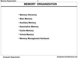
- 1. 1 Memory Organization Computer Organization Computer Architectures Lab • Memory Hierarchy • Main Memory • Auxiliary Memory • Associative Memory • Cache Memory • Virtual Memory • Memory Management Hardware MEMORY ORGANIZATION
- 2. 2 Memory Organization Computer Organization Computer Architectures Lab MEMORY HIERARCHY Magnetic tapes Magnetic disks I/O processor CPU Main memory Cache memory Auxiliary memory Register Cache Main Memory Magnetic Disk Magnetic Tape Memory Hierarchy is to obtain the highest possible access speed while minimizing the total cost of the memory system Memory Hierarchy
- 3. 3 Memory Organization Computer Organization Computer Architectures Lab MAIN MEMORY RAM and ROM Chips Typical RAM chip Typical ROM chip Chip select 1 Chip select 2 Read Write 7-bit address CS1 CS2 RD WR AD 7 128 x 8 RAM 8-bit data bus CS1 CS2 RD WR 0 0 x x 0 1 x x 1 0 0 0 1 0 0 1 1 0 1 x 1 1 x x Memory function Inhibit Inhibit Inhibit Write Read Inhibit State of data bus High-impedence High-impedence High-impedence Input data to RAM Output data from RAM High-impedence Chip select 1 Chip select 2 9-bit address CS1 CS2 AD 9 512 x 8 ROM 8-bit data bus Main Memory
- 4. 4 Memory Organization Computer Organization Computer Architectures Lab MEMORY ADDRESS MAP RAM 1 RAM 2 RAM 3 RAM 4 ROM 0000 - 007F 0080 - 00FF 0100 - 017F 0180 - 01FF 0200 - 03FF Component Hexa address 0 0 0 x x x x x x x 0 0 1 x x x x x x x 0 1 0 x x x x x x x 0 1 1 x x x x x x x 1 x x x x x x x x x 10 9 8 7 6 5 4 3 2 1 Address bus Memory Connection to CPU - RAM and ROM chips are connected to a CPU through the data and address buses - The low-order lines in the address bus select the byte within the chips and other lines in the address bus select a particular chip through its chip select inputs Address space assignment to each memory chip Example: 512 bytes RAM and 512 bytes ROM Main Memory
- 5. 5 Memory Organization Computer Organization Computer Architectures Lab CONNECTION OF MEMORY TO CPU Main Memory } CS1 CS2 RD WR AD7 128 x 8 RAM 1 CS1 CS2 RD WR AD7 128 x 8 RAM 2 CS1 CS2 RD WR AD7 128 x 8 RAM 3 CS1 CS2 RD WR AD7 128 x 8 RAM 4 Decoder 3 2 1 0 WR RD 9 8 7-1 10 16-11 Address bus Data bus CPU CS1 CS2 512 x 8 ROM AD9 1- 7 9 8 Data Data Data Data Data