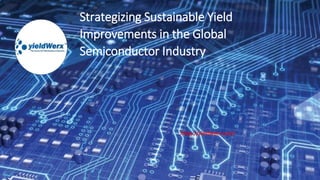
Strategizing Sustainable Yield Improvements in the Global Semiconductor Industry.pptx

The global semiconductor manufacturing industry is facing amplified levels of competition and consolidation. As a result, there's an increasing urgency to drive productivity enhancements that support long-term success. To manage rising cost pressures and augment profitability, semiconductor enterprises need to underline and pursue strategies for end-to-end semiconductor yield improvement. Yield optimization is pivotal to curbing manufacturing costs and securing a competitive advantage. However, many companies find it challenging to attain sustainable yield enhancements due to entrenched mindsets, limited data visibility, compartmentalized efforts, and a paucity of advanced analytics capabilities.As the trend towards miniaturization continues, semiconductor devices are becoming increasingly sophisticated, resulting in an escalated influence of process variability and contaminations on yield. As devices shrink, the impact of any single defect or contamination can become significantly more severe, leading to higher yield losses. Variability in parameters such as temperature, pressure, and timing can lead to inconsistency in device performance, affecting both yield and product quality. Additionally, contaminations can originate from various sources such as materials, process gases, or the manufacturing environment itself, causing defects in the devices that result in yield loss.

Recommended
Recommended
More Related Content
Similar to Strategizing Sustainable Yield Improvements in the Global Semiconductor Industry.pptx
Similar to Strategizing Sustainable Yield Improvements in the Global Semiconductor Industry.pptx (20)
More from yieldWerx Semiconductor
More from yieldWerx Semiconductor (20)
Recently uploaded
Recently uploaded (20)
Strategizing Sustainable Yield Improvements in the Global Semiconductor Industry.pptx
- 1. Strategizing Sustainable Yield Improvements in the Global Semiconductor Industry https://yieldwerx.com/
- 2. The global semiconductor manufacturing industry is facing amplified levels of competition and consolidation. As a result, there's an increasing urgency to drive productivity enhancements that support long-term success. To manage rising cost pressures and augment profitability, semiconductor enterprises need to underline and pursue strategies for end-to-end semiconductor yield improvement. Yield optimization is pivotal to curbing manufacturing costs and securing a competitive advantage. However, many companies find it challenging to attain sustainable yield enhancements due to entrenched mindsets, limited data visibility, compartmentalized efforts, and a paucity of advanced analytics capabilities. As the trend towards miniaturization continues, semiconductor devices are becoming increasingly sophisticated, resulting in an escalated influence of process variability and contaminations on yield. As devices shrink, the impact of any single defect or contamination can become significantly more severe, leading to higher yield losses. Variability in parameters such as temperature, pressure, and timing can lead to inconsistency in device performance, affecting both yield and product quality. Additionally, contaminations can originate from various sources such as materials, process gases, or the manufacturing environment itself, causing defects in the devices that result in yield loss. Data-Driven Improvement Initiatives and Advanced Analytics The era of big data and advanced analytics has provided a new pathway for yield improvement. Advanced analytics can help in predicting yield outcomes, identifying the root causes of yield loss, and formulating strategies for improvement. Semiconductor companies are increasingly leveraging machine learning and data mining techniques to identify patterns and correlations in large datasets, leading to more effective yield enhancement systems. Data-driven initiatives involve the use of data at every stage of the semiconductor manufacturing process. These include real-time data collection during wafer fabrication, statistical analysis of process and test data, as well as predictive modeling of yield and performance metrics. Such initiatives allow for a more holistic view of the manufacturing process, identifying the areas with the greatest loss impact, and directing improvement efforts accordingly.
- 3. Overcoming Limitations of Traditional Yield Improvement Approaches In a world where devices are shrinking in size while becoming technologically sophisticated, the effects of process variability and contaminations on yield are intensifying. Traditional approaches for yield improvement, including focusing on yield percentages, specific product families, or excursion cases, have limitations. While these strategies can capture and control different types of yield losses, they may not exhaust all possibilities for enhancing profitability. Collaboration between Engineering and Finance: A Holistic View of Yield Loss Cost A comprehensive view of yield loss cost requires a collaborative effort between the engineering and finance departments. The engineering department typically focuses on technical aspects such as process optimization, equipment efficiency, and defect reduction. In contrast, the finance department focuses on the financial impacts of yield loss, including the cost of scrapped wafers, rework, and delayed deliveries. By merging cost data from both departments, semiconductor companies can gain a more comprehensive understanding of yield loss costs. This could include the cost of raw materials, energy, labor, and capital equipment, as well as the opportunity costs associated with yield loss. Such a holistic view can facilitate more effective decision-making, resource allocation, and strategic planning for yield improvement. Systemic Improvements: Focus on Machine, Man, Material, Measurement, and Method To achieve sustainable yield improvements, it's crucial to focus on systemic issues rather than isolated problems. This involves a comprehensive focus on the key improvement themes: machine, man, material, measurement, and method. Machine: Machine variability can be a major contributor to yield loss. This can be mitigated through equipment optimization, preventive maintenance, and regular performance and semiconductor yield monitoring. Man: The role of the workforce in yield improvement cannot be underestimated. This includes operator training, skill development, and fostering a culture of continuous improvement. Material: The quality of raw materials and process gases can significantly affect yield. Material quality management and supplier collaboration are key strategies in this regard. Measurement: Accurate and timely measurement of process parameters is crucial for maintaining process control and minimizing variability. Method: Lastly, the methods or processes used in device fabrication need to be continually optimized to improve yield.
- 4. Implementing Systemic Improvements for Sustainable Yield Enhancements Next comes the phase of implementing systemic improvements to counter the recognized loss areas. Engineers concentrate on key improvement themes revolving around five factors - machine, man, material, measurement, and method. True and false rejects are scrutinized, and the potential for cross-functional collaborations is explored. By tackling systemic issues, semiconductor companies can actualize sustainable yield enhancements. In some cases, external involvement could be necessary, especially for machine variability initiatives. These collaborations could involve discussions with vendors to enhance equipment performance. Conclusion In the highly competitive and consolidated semiconductor industry, prioritizing end-to-end yield improvement is a strategic necessity. By adopting a data-driven approach, companies can effectively manage cost pressures, sustain higher profitability, and gain a competitive edge in the industry. Furthermore, a collaboration between engineering and finance departments can provide a more comprehensive view of yield loss costs, enabling more effective decision-making and resource allocation. Systemic improvements, focusing on machine, man, material, measurement, and method, can lead to sustainable yield improvements. Ultimately, success in yield improvement depends on a company's ability to leverage data, advanced analytics, and cross-functional collaboration to drive continuous improvement in its manufacturing processes. References 1. Y. Ye, Q. Xu, and B. Yu, "Machine Learning for Yield Improvement in Semiconductor Manufacturing and an Application to Defect Classification," in 2018 IEEE/ACM International Conference on Computer-Aided Design (ICCAD), San Diego, CA, 2018, pp. 1-6, doi: 10.1145/3240765.3240831. 2. A. El Gamal and M. A. Elmasry, "Process variations and yield," in Analysis and Design of Digital Integrated Circuits, Third Edition, D. A. Hodges, H. G. Jackson, and R. A. Saleh, Eds., 2003. 3. M. Taouil, S. Hamdioui, "Yield Improvement by Tolerating Defects," in 2018 31st International Conference on VLSI Design and 2018 17th International Conference on Embedded Systems (VLSID), pp. 209-214, Jan. 2018, doi: 10.1109/VLSID.2018.00047. 4. S. Borkar, "Designing Reliable Systems from Unreliable Components: The Challenges of Transistor Variability and Degradation," in IEEE Micro, vol. 25, no. 6, pp. 10-16, Nov.-Dec. 2005, doi: 10.1109/MM.2005.110.