SlideShare a Scribd company logo
1 of 37
Download to read offline
Product
Folder
Sample &
Buy
Technical
Documents
Tools &
Software
Support &
Community
LM3488 LM3488-Q1,
SNVS089N –JULY 2000–REVISED
DECEMBER 2014 www.kynix.com
LM3488/-Q1 High-Efficiency, Low-Side, N-Channel Controller for Switching Regulators
1 Features 3 Description
The LM3488 is a versatile low-side N-FET high-1• LM3488-Q1 is AEC-Q100 Qualified and
performance controller for switching regulators. ThisManufactured on an Automotive-Grade Flow
device is suitable for use in topologies requiring low-
• 8-Lead VSSOP Package side FET, such as boost, flyback, or SEPIC.
• Internal Push-Pull Driver With 1-A Peak Current Moreover, the LM3488 can be operated at extremely
high switching frequency to reduce the overallCapability
solution size. The switching frequency of LM3488 can• Current Limit and Thermal Shutdown
be adjusted to any value from 100 kHz to 1 MHz by
• Frequency Compensation Optimized With a using a single external resistor or by synchronizing it
Capacitor and a Resistor to an external clock. Current mode control provides
• Internal Soft-Start superior bandwidth and transient response, besides
cycle-by-cycle current limiting. Output current can be• Current Mode Operation
programmed with a single external resistor.
• Undervoltage Lockout With Hysteresis
The LM3488 has built-in features such as thermal• Key Specifications:
shutdown, short-circuit protection, and overvoltage
– Wide Supply Voltage Range of 2.97 V to 40 V protection. Power-saving shutdown mode reduces the
– 100-kHz to 1-MHz Adjustable and total supply current to 5 µA and allows power supply
sequencing. Internal soft-start limits the inrush currentSynchronizable Clock Frequency
at start-up.– ±1.5% (Overtemperature) Internal Reference
– 5-µA Shutdown Current (Overtemperature) Device Information(1)
PART NUMBER PACKAGE BODY SIZE (NOM)
2 Applications
LM3488
VSSOP (8) 3.00 mm × 3.00 mm• Distributed Power Systems LM3488-Q1
• Notebook, PDA, Digital Camera, and other (1) For all available packages, see the orderable addendum at
Portable Applications the end of the datasheet.
• Offline Power Supplies
• Set-Top Boxes
Typical SEPIC Converter
1
An IMPORTANT NOTICE at the end of this data sheet addresses availability, warranty, changes, use in safety-critical applications,
intellectual property matters and other important disclaimers. PRODUCTION DATA.
LM3488, LM3488-Q1
SNVS089N –JULY 2000–REVISED DECEMBER 2014 www.ti.com
Table of Contents
7.3 Feature Description................................................. 121 Features.................................................................. 1
7.4 Device Functional Modes........................................ 162 Applications ........................................................... 1
8 Application and Implementation ........................ 173 Description ............................................................. 1
8.1 Application Information............................................ 174 Revision History..................................................... 2
8.2 Typical Applications ................................................ 17
5 Pin Configuration and Functions......................... 3
9 Power Supply Recommendations...................... 286 Specifications......................................................... 3
10 Layout................................................................... 286.1 Absolute Maximum Ratings ..................................... 3
10.1 Layout Guidelines ................................................. 286.2 Handling Ratings : LM3488....................................... 4
10.2 Layout Example .................................................... 296.3 Handling Ratings: LM3488-Q1.................................. 4
11 Device and Documentation Support ................. 296.4 Recommended Operating Conditions....................... 4
11.1 Related Links ........................................................ 296.5 Thermal Information.................................................. 4
11.2 Trademarks........................................................... 306.6 Electrical Characteristics........................................... 4
11.3 Electrostatic Discharge Caution............................ 306.7 Typical Characteristics.............................................. 7
11.4 Glossary................................................................ 307 Detailed Description ............................................ 11
12 Mechanical, Packaging, and Orderable7.1 Overview ................................................................. 11
Information ........................................................... 307.2 Functional Block Diagram ....................................... 12
4 Revision History
Changes from Revision M (March 2013) to Revision N Page
• Added Pin Configuration and Functions section, Handling Rating table, Feature Description section, Device
Functional Modes, Application and Implementation section, Power Supply Recommendations section, Layout
section, Device and Documentation Support section, and Mechanical, Packaging, and Orderable Information
section ................................................................................................................................................................................... 1
Changes from Revision L (March 2013) to Revision M Page
• Changed layout of National Data Sheet to TI format .......................................................................................................... 29
2 Submit Documentation Feedback Copyright © 2000–2014, Texas Instruments Incorporated
Product Folder Links: LM3488 LM3488-Q1
LM3488, LM3488-Q1
www.ti.com SNVS089N –JULY 2000–REVISED DECEMBER 2014
5 Pin Configuration and Functions
8-Pin DGK
VSSOP Package
Top View
Pin Functions
PIN
TYPE DESCRIPTION
NAME NO.
ISEN 1 I Current sense input pin. Voltage generated across an external sense resistor is fed into this pin.
COMP 2 A Compensation pin. A resistor, capacitor combination connected to this pin provides compensation for the
control loop.
FB 3 I Feedback pin. The output voltage should be adjusted using a resistor divider to provide 1.26 V at this pin.
AGND 4 P Analog ground pin.
PGND 5 P Power ground pin.
DR 6 O Drive pin of the IC. The gate of the external MOSFET should be connected to this pin.
FA/SYNC/S 7 A Frequency adjust, synchronization, and Shutdown pin. A resistor connected to this pin sets the oscillator
D frequency. An external clock signal at this pin will synchronize the controller to the frequency of the clock.
A high level on this pin for ≥ 30 µs will turn the device off. The device will then draw less than 10µA from
the supply.
VIN 8 P Power supply input pin.
6 Specifications
6.1 Absolute Maximum Ratings (1)
MIN MAX UNIT
Input voltage 45 V
FB pin voltage –0.4 < VFB VFB < 7 V
FA/SYNC/SD pin voltage –0.4 < VFA/SYNC/SD VFA/SYNC/SD < 7 V
Peak driver output current (< 10 µs) 1 A
Power dissipation Internally Limited
Junction temperature 150 °C
Lead temperature Vapor Phase (60 s) 215 °C
Infared (15 s) 260 °C
DR pin voltage −0.4 ≤ VDR VDR ≤ 8 V
ILIM pin voltage 600 mV
(1) Absolute Maximum Ratings are limits beyond which damage to the device may occur. Recommended Operating Conditions are
conditions under which operation of the device is intended to be functional. For specifications and test conditions, see the Electrical
Characteristics.
Copyright © 2000–2014, Texas Instruments Incorporated Submit Documentation Feedback 3
Product Folder Links: LM3488 LM3488-Q1
LM3488, LM3488-Q1
SNVS089N –JULY 2000–REVISED DECEMBER 2014 www.ti.com
6.2 Handling Ratings : LM3488
MIN MAX UNIT
Tstg Storage temperature range –65 150 °C
Human body model (HBM), per ANSI/ESDA/JEDEC JS-001, all –2000 2000
pins(1)
V(ESD) Electrostatic discharge V
Charged device model (CDM), per JEDEC specification –750 750
JESD22-C101, all pins(2)
(1) JEDEC document JEP155 states that 500-V HBM allows safe manufacturing with a standard ESD control process.
(2) JEDEC document JEP157 states that 250-V CDM allows safe manufacturing with a standard ESD control process.
6.3 Handling Ratings: LM3488-Q1
MIN MAX UNIT
Tstg Storage temperature range –65 150 °C
Human body model (HBM), per AEC Q100-002(1)
–2000 2000
Corner pins (1, 4, 5, –750 750
V(ESD) Electrostatic discharge VCharged device model (CDM), per and 8)
AEC Q100-011
Other pins –750 750
(1) AEC Q100-002 indicates HBM stressing is done in accordance with the ANSI/ESDA/JEDEC JS-001 specification.
6.4 Recommended Operating Conditions
MIN MAX UNIT
Supply Voltage 2.97 ≤ VIN VIN ≤ 40 V
Junction Temperature Range −40 ≤ TJ TJ ≤ 125 °C
Switching Frequency 100 ≤ FSW FSW ≤ 1 kHz/MH
z
6.5 Thermal Information
LM3488,
LM3488-Q1
THERMAL METRIC(1)
UNIT
DGK
8 PINS
RθJA Junction-to-ambient thermal resistance 160
RθJC(top) Junction-to-case (top) thermal resistance 50
RθJB Junction-to-board thermal resistance 77 °C/W
ψJT Junction-to-top characterization parameter 4.7
ψJB Junction-to-board characterization parameter 76
(1) For more information about traditional and new thermal metrics, see the IC Package Thermal Metrics application report, SPRA953.
6.6 Electrical Characteristics
Unless otherwise specified, VIN = 12 V, RFA = 40 kΩ, TJ = 25°C
PARAMETER TEST CONDITIONS MIN TYP MAX UNIT
VFB Feedback Voltage VCOMP = 1.4 V, 2.97 ≤ VIN ≤ 40 V 1.2507 1.26 1.2753 V
VCOMP = 1.4 V, 2.97 ≤ VIN ≤ 40 V, 1.24 1.28
−40°C ≤ TJ ≤ 125°C
ΔVLINE Feedback Voltage Line Regulation 2.97 ≤ VIN ≤ 40 V 0.001 %/V
ΔVLOAD Output Voltage Load Regulation IEAO Source/Sink ±0.5 %/V
(max)
VUVLO Input Undervoltage Lock-out 2.85 V
−40°C ≤ TJ ≤ 125°C 2.97
VUV(HYS) Input Undervoltage Lock-out Hysteresis 170 mV
−40°C ≤ TJ ≤ 125°C 130 210
4 Submit Documentation Feedback Copyright © 2000–2014, Texas Instruments Incorporated
Product Folder Links: LM3488 LM3488-Q1
LM3488, LM3488-Q1
www.ti.com SNVS089N –JULY 2000–REVISED DECEMBER 2014
Electrical Characteristics (continued)
Unless otherwise specified, VIN = 12 V, RFA = 40 kΩ, TJ = 25°C
PARAMETER TEST CONDITIONS MIN TYP MAX UNIT
Fnom Nominal Switching Frequency RFA = 40 KΩ 400 kHz
RFA = 40 KΩ, −40°C ≤ TJ ≤ 125°C 360 430
RDS1 (ON) Driver Switch On Resistance (top) IDR = 0.2A, VIN= 5 V 16 Ω
RDS2 (ON) Driver Switch On Resistance (bottom) IDR = 0.2A 4.5 Ω
VDR (max) Maximum Drive Voltage Swing(1)
VIN < 7.2 V VIN V
VIN ≥ 7.2 V 7.2
Dmax Maximum Duty Cycle(2)
100%
Tmin (on) Minimum On Time 325 nsec
−40°C ≤ TJ ≤ 125°C 230 550
ISUPPLY Supply Current (switching) See (3)
2.7 mA
See (3)
, −40°C ≤ TJ ≤ 125°C 3.0
IQ Quiescent Current in Shutdown Mode VFA/SYNC/SD = 5 V(4)
, VIN = 5 V 5 µA
VFA/SYNC/SD = 5 V(4)
, VIN = 5 V, 7
−40°C ≤ TJ ≤ 125°C
VSENSE Current Sense Threshold Voltage VIN = 5 V 135 156 180 mV
VIN = 5 V, −40°C ≤ TJ ≤ 125°C 125 190
VSC Short-Circuit Current Limit Sense Voltage VIN = 5 V 343 mV
VIN = 5 V, −40°C ≤ TJ ≤ 125°C 250 415
VSL Internal Compensation Ramp Voltage VIN = 5 V 92 mV
VIN = 5 V, −40°C ≤ TJ ≤ 125°C 52 132
VSL ratio VSL/VSENSE 0.30 0.49 0.70
VOVP Output Overvoltage Protection (with VCOMP = 1.4 V 32 50 78 mV
respect to feedback voltage) (5)
VCOMP = 1.4 V, −40°C ≤ TJ ≤ 25 85
125°C
VOVP(HYS) Output Over-Voltage Protection VCOMP = 1.4 V 60 mV
Hysteresis(5)
VCOMP = 1.4 V, −40°C ≤ TJ ≤ 20 110
125°C
Gm Error Ampifier Transconductance VCOMP = 1.4 V, IEAO = 100 µA 600 800 1000 µmho
(Source/Sink)
VCOMP = 1.4 V, IEAO = 100 µA 365 1265
(Source/Sink), −40°C ≤ TJ ≤ 125°C
AVOL Error Amplifier Voltage Gain VCOMP = 1.4 V, IEAO = 100 µA 38 V/V
(Source/Sink)
VCOMP = 1.4 V, IEAO = 100 µA 26 44
(Source/Sink), −40°C ≤ TJ ≤ 125°C
IEAO Error Amplifier Output Current (Source/ Source, VCOMP = 1.4 V, VFB = 0 V 80 110 140 µA
Sink)
Source, VCOMP = 1.4 V, VFB = 0 V, 50 180
−40°C ≤ TJ ≤ 125°C
Sink, VCOMP = 1.4 V, VFB = 1.4 V −100 −140 −180 µA
Sink, VCOMP = 1.4 V, VFB = 1.4 V, −85 −185
−40°C ≤ TJ ≤ 125°C
(1) The voltage on the drive pin, VDR is equal to the input voltage when input voltage is less than 7.2 V. VDR is equal to 7.2 V when the
input voltage is greater than or equal to 7.2 V.
(2) The limits for the maximum duty cycle can not be specified since the part does not permit less than 100% maximum duty cycle
operation.
(3) For this test, the FA/SYNC/SD Pin is pulled to ground using a 40K resistor .
(4) For this test, the FA/SYNC/SD Pin is pulled to 5 V using a 40K resistor.
(5) The over-voltage protection is specified with respect to the feedback voltage. This is because the over-voltage protection tracks the
feedback voltage. The over-voltage thresold can be calculated by adding the feedback voltage, VFB to the over-voltage protection
specification.
Copyright © 2000–2014, Texas Instruments Incorporated Submit Documentation Feedback 5
Product Folder Links: LM3488 LM3488-Q1
LM3488, LM3488-Q1
SNVS089N –JULY 2000–REVISED DECEMBER 2014 www.ti.com
Electrical Characteristics (continued)
Unless otherwise specified, VIN = 12 V, RFA = 40 kΩ, TJ = 25°C
PARAMETER TEST CONDITIONS MIN TYP MAX UNIT
VEAO Error Amplifier Output Voltage Swing Upper Limit: VFB = 0 V, COMP Pin 2.2 V
= Floating
Upper Limit: VFB = 0 V, COMP Pin 1.8 2.4
= Floating, −40°C ≤ TJ ≤ 125°C
Lower Limit: VFB = 1.4 V 0.56 V
Lower Limit: VFB = 1.4 V, −40°C ≤ 0.2 1.0
TJ ≤ 125°C
TSS Internal Soft-Start Delay VFB = 1.2 V, VCOMP = Floating 4 ms
Tr Drive Pin Rise Time Cgs = 3000 pf, VDR = 0 to 3 V 25 ns
Tf Drive Pin Fall Time Cgs = 3000 pf, VDR = 0 to 3 V 25 ns
VSD Shutdown and Synchronization signal Output = High 1.27 V
threshold (6)
Output = High, −40°C ≤ TJ ≤ 125°C 1.4
Output = Low 0.65 V
Output = Low, −40°C ≤ TJ ≤ 125°C 0.3
ISD Shutdown Pin Current VSD = 5 V −1 µA
VSD = 0 V +1
IFB Feedback Pin Current 15 nA
TSD Thermal Shutdown 165 °C
Tsh Thermal Shutdown Hysteresis 10 °C
(6) The FA/SYNC/SD pin should be pulled to VIN through a resistor to turn the regulator off.
6 Submit Documentation Feedback Copyright © 2000–2014, Texas Instruments Incorporated
Product Folder Links: LM3488 LM3488-Q1
LM3488, LM3488-Q1
www.ti.com SNVS089N –JULY 2000–REVISED DECEMBER 2014
6.7 Typical Characteristics
Unless otherwise specified, VIN = 12V, TJ = 25°C.
Figure 1. IQ vs Temperature & Input Voltage Figure 2. ISupply vs Input Voltage (Non-Switching)
Figure 3. ISupply vs VIN Figure 4. Switching Frequency vs RFA
Figure 5. Frequency vs Temperature Figure 6. Drive Voltage vs Input Voltage
Copyright © 2000–2014, Texas Instruments Incorporated Submit Documentation Feedback 7
Product Folder Links: LM3488 LM3488-Q1
LM3488, LM3488-Q1
SNVS089N –JULY 2000–REVISED DECEMBER 2014 www.ti.com
Typical Characteristics (continued)
Unless otherwise specified, VIN = 12V, TJ = 25°C.
Figure 7. Current Sense Threshold vs Input Voltage Figure 8. COMP Pin Voltage vs Load Current
Figure 9. Efficiency vs Load Current (3.3 V In and 12 V Out) Figure 10. Efficiency vs Load Current (5 V In and 12 V Out)
Figure 12. Efficiency vs Load Current (3.3 V In and 5 V Out)Figure 11. Efficiency vs Load Current (9 V In and 12 V Out)
8 Submit Documentation Feedback Copyright © 2000–2014, Texas Instruments Incorporated
Product Folder Links: LM3488 LM3488-Q1
LM3488, LM3488-Q1
www.ti.com SNVS089N –JULY 2000–REVISED DECEMBER 2014
Typical Characteristics (continued)
Unless otherwise specified, VIN = 12V, TJ = 25°C.
Figure 13. Error Amplifier Gain Figure 14. Error Amplifier Phase
Figure 16. Short Circuit Protection vs Input VoltageFigure 15. COMP Pin Source Current vs Temperature
Figure 18. Shutdown Threshold Hysteresis vs TemperatureFigure 17. Compensation Ramp vs Compensation Resistor
Copyright © 2000–2014, Texas Instruments Incorporated Submit Documentation Feedback 9
Product Folder Links: LM3488 LM3488-Q1
LM3488, LM3488-Q1
SNVS089N –JULY 2000–REVISED DECEMBER 2014 www.ti.com
Typical Characteristics (continued)
Unless otherwise specified, VIN = 12V, TJ = 25°C.
Figure 19. Current Sense Voltage vs Duty Cycle
10 Submit Documentation Feedback Copyright © 2000–2014, Texas Instruments Incorporated
Product Folder Links: LM3488 LM3488-Q1
LM3488, LM3488-Q1
www.ti.com SNVS089N –JULY 2000–REVISED DECEMBER 2014
7 Detailed Description
7.1 Overview
The LM3488 uses a fixed frequency, Pulse Width Modulated (PWM), current mode control architecture. In a
typical application circuit, the peak current through the external MOSFET is sensed through an external sense
resistor. The voltage across this resistor is fed into the ISEN pin. This voltage is then level shifted and fed into the
positive input of the PWM comparator. The output voltage is also sensed through an external feedback resistor
divider network and fed into the error amplifier negative input (feedback pin, FB). The output of the error amplifier
(COMP pin) is added to the slope compensation ramp and fed into the negative input of the PWM comparator.
At the start of any switching cycle, the oscillator sets the RS latch using the SET/Blank-out and switch logic
blocks. This forces a high signal on the DR pin (gate of the external MOSFET) and the external MOSFET turns
on. When the voltage on the positive input of the PWM comparator exceeds the negative input, the RS latch is
reset and the external MOSFET turns off.
The voltage sensed across the sense resistor generally contains spurious noise spikes, as shown in Figure 20.
These spikes can force the PWM comparator to reset the RS latch prematurely. To prevent these spikes from
resetting the latch, a blank-out circuit inside the IC prevents the PWM comparator from resetting the latch for a
short duration after the latch is set. This duration is about 150ns and is called the blank-out time.
Under extremely light load or no-load conditions, the energy delivered to the output capacitor when the external
MOSFET is on during the blank-out time is more than what is delivered to the load. An over-voltage comparator
inside the LM3488 prevents the output voltage from rising under these conditions. The over-voltage comparator
senses the feedback (FB pin) voltage and resets the RS latch under these conditions. The latch remains in reset
state till the output decays to the nominal value.
Figure 20. Basic Operation of the PWM Comparator
Copyright © 2000–2014, Texas Instruments Incorporated Submit Documentation Feedback 11
Product Folder Links: LM3488 LM3488-Q1
LM3488, LM3488-Q1
SNVS089N –JULY 2000–REVISED DECEMBER 2014 www.ti.com
7.2 Functional Block Diagram
7.3 Feature Description
7.3.1 Slope Compensation Ramp
The LM3488 uses a current mode control scheme. The main advantages of current mode control are inherent
cycle-by-cycle current limit for the switch, and simpler control loop characteristics. It is also easy to parallel power
stages using current mode control since as current sharing is automatic.
Current mode control has an inherent instability for duty cycles greater than 50%, as shown in Figure 21. In
Figure 21, a small increase in the load current causes the switch current to increase by ΔIO. The effect of this
load change, ΔI1, is :
(1)
From the above equation, when D > 0.5, ΔI1 will be greater than ΔIO. In other words, the disturbance is divergent.
So a very small perturbation in the load will cause the disturbance to increase.
To prevent the sub-harmonic oscillations, a compensation ramp is added to the control signal, as shown in
Figure 22.
12 Submit Documentation Feedback Copyright © 2000–2014, Texas Instruments Incorporated
Product Folder Links: LM3488 LM3488-Q1
MC =
40x10-6 .
RSL
.
FS
RSEN
Amps
second
LM3488, LM3488-Q1
www.ti.com SNVS089N –JULY 2000–REVISED DECEMBER 2014
Feature Description (continued)
With the compensation ramp,
(2)
Figure 21. Sub-Harmonic Oscillation for D0.5
Figure 22. Compensation Ramp Avoids Sub-Harmonic Oscillation
The compensation ramp has been added internally in LM3488. The slope of this compensation ramp has been
selected to satisfy most of the applications. The slope of the internal compensation ramp depends on the
frequency. This slope can be calculated using the formula:
MC = VSL.FS Volts/second (3)
In the above equation, VSL is the amplitude of the internal compensation ramp. Limits for VSL have been specified
in the electrical characteristics.
In order to provide the user additional flexibility, a patented scheme has been implemented inside the IC to
increase the slope of the compensation ramp externally, if the need arises. Adding a single external resistor,
RSL(as shown in Figure 23) increases the slope of the compensation ramp, MC by :
(4)
In this equation, ΔVSL is equal to 40.10-6
RSL. Hence,
(5)
ΔVSL versus RSL has been plotted in Figure 24 for different frequencies.
Copyright © 2000–2014, Texas Instruments Incorporated Submit Documentation Feedback 13
Product Folder Links: LM3488 LM3488-Q1
LM3488, LM3488-Q1
SNVS089N –JULY 2000–REVISED DECEMBER 2014 www.ti.com
Feature Description (continued)
Figure 23. Increasing the Slope of the Compensation Ramp
Figure 24. ΔVSL vs RSL
7.3.2 Frequency Adjust/Synchronization/Shutdown
The switching frequency of LM3488 can be adjusted between 100kHz and 1MHz using a single external resistor.
This resistor must be connected between FA/SYNC/SD pin and ground, as shown in Figure 25. See Typical
Characteristics to determine the value of the resistor required for a desired switching frequency.
The LM3488 can be synchronized to an external clock. The external clock must be connected to the
FA/SYNC/SD pin through a resistor, RSYNC as shown in Figure 26. The value of this resistor is dependent on the
off time of the synchronization pulse, TOFF(SYNC). Table 1 shows the range of resistors to be used for a given
TOFF(SYNC).
Table 1. Recommended Series Resistance for
Synchronization
TOFF(SYNC) (µs) RSYNC range (kΩ)
1 5 to 13
2 20 to 40
14 Submit Documentation Feedback Copyright © 2000–2014, Texas Instruments Incorporated
Product Folder Links: LM3488 LM3488-Q1
LM3488, LM3488-Q1
www.ti.com SNVS089N –JULY 2000–REVISED DECEMBER 2014
Table 1. Recommended Series Resistance for
Synchronization (continued)
TOFF(SYNC) (µs) RSYNC range (kΩ)
3 40 to 65
4 55 to 90
5 70 to 110
6 85 to 140
7 100 to 160
8 120 to 190
9 135 to 215
10 150 to 240
It is also necessary to have the width of the synchronization pulse wider than the duty cycle of the converter
(when DR pin is high and the switching point is low). It is also necessary to have the synchronization pulse width
≥ 300nsecs.
The FA/SYNC/SD pin also functions as a shutdown pin. If a high signal (see Electrical Characteristics for
definition of high signal) appears on the FA/SYNC/SD pin, the LM3488 stops switching and goes into a low
current mode. The total supply current of the IC reduces to less than 10µA under these conditions.
Figure 27 and Figure 28 show implementation of shutdown function when operating in Frequency adjust mode
and synchronization mode respectively. In frequency adjust mode, connecting the FA/SYNC/SD pin to ground
forces the clock to run at a certain frequency. Pulling this pin high shuts down the IC. In frequency adjust or
synchronization mode, a high signal for more than 30µs shuts down the IC.
Figure 29 shows implementation of both frequency adjust with RFA resistor and frequency synchronization with
RSYNC. The switching frequency is defined by RFA when a synchronization signal is not applied. When sync is
applied it overrides the RFA setting.
Figure 25. Frequency Adjust
Figure 26. Frequency Synchronization
Copyright © 2000–2014, Texas Instruments Incorporated Submit Documentation Feedback 15
Product Folder Links: LM3488 LM3488-Q1
LM3488
FA/SYNC/SD
RFA
RSYNC CSYNC
270 pF
LM3488, LM3488-Q1
SNVS089N –JULY 2000–REVISED DECEMBER 2014 www.ti.com
Figure 27. Shutdown Operation in Frequency Adjust Mode
Figure 28. Shutdown Operation in Synchronization Mode
Figure 29. Frequency Adjust or Frequency Synchronization
7.3.3 Short-Circuit Protection
When the voltage across the sense resistor (measured on ISEN Pin) exceeds 350mV, short-circuit current limit
gets activated. A comparator inside LM3488 reduces the switching frequency by a factor of 5 and maintains this
condition till the short is removed.
7.4 Device Functional Modes
The device is set to run as soon as the input voltage crosses above the UVLO set point and at a frequency set
according to the FA/SYNC/SD pin pull-down resistor or to run at a frequency set by the waveform applied to the
FA/SYNC/SD pin.
If the FA/SYNC/SD pin is pulled high, the LM3488 enters shut-down mode.
If the voltage at the ISEN pin exceeds Vsc, the device enters short-circuit protection mode.
16 Submit Documentation Feedback Copyright © 2000–2014, Texas Instruments Incorporated
Product Folder Links: LM3488 LM3488-Q1
20k
RF1
CC 22 nF
RC
4.7k
AGND
FB
COMP
ISEN
RFA
40k
VIN
FA/SD/SYNC
DR
PGND
L
10 PH
0.025:
RSN
Q1
IRF7807
D MBRD340
CIN
100 PF, 6.3V
+
VIN = 3.3V (±10%)
60k
RF2
COUT
100 PF, 10V
+
x2
VOUT = 5V, 2A
CSN
0.01 PF
LM3488
LM3488, LM3488-Q1
www.ti.com SNVS089N –JULY 2000–REVISED DECEMBER 2014
8 Application and Implementation
NOTE
Information in the following applications sections is not part of the TI component
specification, and TI does not warrant its accuracy or completeness. TI’s customers are
responsible for determining suitability of components for their purposes. Customers should
validate and test their design implementation to confirm system functionality.
8.1 Application Information
The LM3488 may be operated in either continuous or discontinuous conduction mode. The following applications
are designed for continuous conduction operation. This mode of operation has higher efficiency and lower EMI
characteristics than the discontinuous mode.
8.2 Typical Applications
8.2.1 Boost Converter
Figure 30. Typical High Efficiency Step-Up (Boost) Converter
The most common topology for LM3488 is the boost or step-up topology. The boost converter converts a low
input voltage into a higher output voltage. The basic configuration for a boost regulator is shown in Figure 31. In
continuous conduction mode (when the inductor current never reaches zero at steady state), the boost regulator
operates in two cycles. In the first cycle of operation, MOSFET Q is turned on and energy is stored in the
inductor. During this cycle, diode D is reverse biased and load current is supplied by the output capacitor, COUT.
Copyright © 2000–2014, Texas Instruments Incorporated Submit Documentation Feedback 17
Product Folder Links: LM3488 LM3488-Q1
LM3488, LM3488-Q1
SNVS089N –JULY 2000–REVISED DECEMBER 2014 www.ti.com
Typical Applications (continued)
Figure 31. Simplified Boost Converter Diagram
(a) First cycle of operation
(b) Second cycle of operation
In the second cycle, MOSFET Q is off and the diode is forward biased. The energy stored in the inductor is
transferred to the load and output capacitor. The ratio of these two cycles determines the output voltage. The
output voltage is defined as:
(6)
(ignoring the drop across the MOSFET and the diode), or
where
• D is the duty cycle of the switch
• VD is the forward voltage drop of the diode
• VQ is the drop across the MOSFET when it is on (7)
8.2.1.1 Design Requirements
To calculate component values for a Boost converter, the power supply parameters shown in Table 2 should be
known. The design shown in Figure 30 is the result of starting with example values shown in Table 2.
Table 2. Boost Design Parameters
DESIGN PARAMETER EXAMPLE VALUE
Input voltage range 3V to 3.6V
Output voltage 5V
Maximum current 2A
Operating frequency 350kHz
18 Submit Documentation Feedback Copyright © 2000–2014, Texas Instruments Incorporated
Product Folder Links: LM3488 LM3488-Q1
t (s)
IL_AVG
ISW_AVG
D*Ts Ts
D*Ts Ts
IL (A)
ID (A)
L
VIN
L
VV OUTIN 

L
VV OUTIN -
(a)
(b)
ISW (A)
(C)
ID_AVG
=IOUT_AVG
t (s)
t (s)
D*Ts Ts
L
VIN
iL
LM3488, LM3488-Q1
www.ti.com SNVS089N –JULY 2000–REVISED DECEMBER 2014
8.2.1.2 Detailed Design Procedure
8.2.1.2.1 Power Inductor Selection
The inductor is one of the two energy storage elements in a boost converter. Figure 32 shows how the inductor
current varies during a switching cycle. The current through an inductor is quantified as:
(8)
Figure 32. A. Inductor Current B. Diode Current C. Switch Current
If VL(t) is constant, diL(t)/dt must be constant. Hence, for a given input voltage and output voltage, the current in
the inductor changes at a constant rate.
The important quantities in determining a proper inductance value are IL (the average inductor current) and ΔiL
(the inductor current ripple). If ΔiL is larger than IL, the inductor current will drop to zero for a portion of the cycle
and the converter will operate in discontinuous conduction mode. If ΔiL is smaller than IL, the inductor current will
stay above zero and the converter will operate in continuous conduction mode. All the analysis in this datasheet
assumes operation in continuous conduction mode. To operate in continuous conduction mode, the following
conditions must be met:
IL  ΔiL (9)
(10)
(11)
Copyright © 2000–2014, Texas Instruments Incorporated Submit Documentation Feedback 19
Product Folder Links: LM3488 LM3488-Q1
DR
VOUT
FB
L
D
Q
ISEN
COUT
Rfb2
VIN
LM3488
RSEN
Rfb1
VOUT = 1.26(1+
RF1
RF2
(
2fSL
iL =
DVIN
LM3488, LM3488-Q1
SNVS089N –JULY 2000–REVISED DECEMBER 2014 www.ti.com
Choose the minimum IOUT to determine the minimum L. A common choice is to set ΔiL to 30% of IL. Choosing an
appropriate core size for the inductor involves calculating the average and peak currents expected through the
inductor. In a boost converter,
(12)
and IL_peak = IL(max) + ΔiL(max),
where
(13)
A core size with ratings higher than these values should be chosen. If the core is not properly rated, saturation
will dramatically reduce overall efficiency.
The LM3488 can be set to switch at very high frequencies. When the switching frequency is high, the converter
can be operated with very small inductor values. With a small inductor value, the peak inductor current can be
extremely higher than the output currents, especially under light load conditions.
The LM3488 senses the peak current through the switch. The peak current through the switch is the same as the
peak current calculated above.
8.2.1.2.2 Programming the Output Voltage
The output voltage can be programmed using a resistor divider between the output and the feedback pins, as
shown in Figure 33. The resistors are selected such that the voltage at the feedback pin is 1.26V. RF1 and RF2
can be selected using the equation,
(14)
A 100-pF capacitor may be connected between the feedback and ground pins to reduce noise.
Figure 33. Adjusting the Output Voltage
20 Submit Documentation Feedback Copyright © 2000–2014, Texas Instruments Incorporated
Product Folder Links: LM3488 LM3488-Q1
RSL 
40 2A
RSEN x (Vo - 2VIN)
2 x fS x L
- VSL
RSEN 
2 x VSL x fS x L
Vo - (2 x VIN)
RSEN =
VSENSE - (D x VSENSE x VSLratio)
ISWLIMIT
ISWLIMIT =
IOUT
(1-D)
+
(D x VIN)
(2 x fS x L)
RSEN =
VSENSE - (D x VSL)
ISWLIMIT
LM3488, LM3488-Q1
www.ti.com SNVS089N –JULY 2000–REVISED DECEMBER 2014
8.2.1.2.3 Setting the Current Limit
The maximum amount of current that can be delivered to the load is set by the sense resistor, RSEN. Current limit
occurs when the voltage that is generated across the sense resistor equals the current sense threshold voltage,
VSENSE. When this threshold is reached, the switch will be turned off until the next cycle. Limits for VSENSE are
specified in Electrical Characteristics. VSENSE represents the maximum value of the internal control signal VCS.
This control signal, however, is not a constant value and changes over the course of a period as a result of the
internal compensation ramp (see Figure 20). Therefore the current limit threshold will also change. The actual
current limit threshold is a function of the sense voltage (VSENSE) and the internal compensation ramp:
RSEN x ISWLIMIT = VCSMAX = VSENSE - (D x VSL)
where
• ISWLIMIT is the peak switch current limit, defined by the equation below. As duty cycle increases, the control
voltage is reduced as VSL ramps up. Since current limit threshold varies with duty cycle, the following equation
should be used to select RSEN and set the desired current limit threshold: (15)
(16)
The numerator of the above equation is VCS, and ISWLIMIT is calculated as:
(17)
To avoid false triggering, the current limit value should have some margin above the maximum operating value,
typically 120%. Values for both VSENSE and VSL are specified in Electrical Characteristics. However, calculating
with the limits of these two specs could result in an unrealistically wide current limit or RSEN range. Therefore, the
following equation is recommended, using the VSL ratio value given in Electrical Characteristics:
(18)
RSEN is part of the current mode control loop and has some influence on control loop stability. Therefore, once
the current limit threshold is set, loop stability must be verified. To verify stability, use the following equation:
(19)
If the selected RSEN is greater than this value, additional slope compensation must be added to ensure stability,
as described in Current Limit with External Slope Compensation.
8.2.1.2.4 Current Limit with External Slope Compensation
RSL is used to add additional slope compensation when required. It is not necessary in most designs and RSL
should be no larger than necessary. Select RSL according to the following equation:
where
• RSEN is the selected value based on current limit. With RSL installed, the control signal includes additional
external slope to stabilize the loop, which will also have an effect on the current limit threshold. Therefore, the
current limit threshold must be re-verified, as illustrated in the equations below : (20)
VCS = VSENSE – (D x (VSL + ΔVSL))
where
• ΔVSL is the additional slope compensation generated and calculated as: (21)
ΔVSL = 40 µA x RSL (22)
Copyright © 2000–2014, Texas Instruments Incorporated Submit Documentation Feedback 21
Product Folder Links: LM3488 LM3488-Q1
RSEN =
VSENSE
Vo - Vi
L x fS
x DISWLIMIT +
ISWLIMIT =
VSENSE - (D x(VSL + VSL))
RSEN
LM3488, LM3488-Q1
SNVS089N –JULY 2000–REVISED DECEMBER 2014 www.ti.com
This changes the equation for current limit (or RSEN) to:
(23)
The RSEN and RSL values may have to be calculated iteratively in order to achieve both the desired current limit
and stable operation. In some designs RSL can also help to filter noise on the ISEN pin.
If the inductor is selected such that ripple current is the recommended 30% value, and the current limit threshold
is 120% of the maximum peak, a simpler method can be used to determine RSEN. The equation below will
provide optimum stability without RSL, provided that the above 2 conditions are met:
(24)
8.2.1.2.5 Power Diode Selection
Observation of the boost converter circuit shows that the average current through the diode is the average load
current, and the peak current through the diode is the peak current through the inductor. The diode should be
rated to handle more than its peak current. The peak diode current can be calculated using the formula:
ID(Peak) = IOUT/ (1−D) + ΔIL (25)
In the above equation, IOUT is the output current and ΔIL has been defined in Figure 32.
The peak reverse voltage for boost converter is equal to the regulator output voltage. The diode must be capable
of handling this voltage. To improve efficiency, a low forward drop schottky diode is recommended.
8.2.1.2.6 Power MOSFET Selection
The drive pin of LM3488 must be connected to the gate of an external MOSFET. In a boost topology, the drain of
the external N-Channel MOSFET is connected to the inductor and the source is connected to the ground. The
drive pin (DR) voltage depends on the input voltage (see the Typical Characteristics section). In most
applications, a logic level MOSFET can be used. For very low input voltages, a sub-logic level MOSFET should
be used.
The selected MOSFET directly controls the efficiency. The critical parameters for selection of a MOSFET are:
1. Minimum threshold voltage, VTH(MIN)
2. On-resistance, RDS(ON)
3. Total gate charge, Qg
4. Reverse transfer capacitance, CRSS
5. Maximum drain to source voltage, VDS(MAX)
The off-state voltage of the MOSFET is approximately equal to the output voltage. VDS(MAX) of the MOSFET must
be greater than the output voltage. The power losses in the MOSFET can be categorized into conduction losses
and ac switching or transition losses. RDS(ON) is needed to estimate the conduction losses. The conduction loss,
PCOND, is the I2
R loss across the MOSFET. The maximum conduction loss is given by:
where
• DMAX is the maximum duty cycle.
(26)
(27)
The turn-on and turn-off transitions of a MOSFET require times of tens of nano-seconds. CRSS and Qg are
needed to estimate the large instantaneous power loss that occurs during these transitions.
The amount of gate current required to turn the MOSFET on can be calculated using the formula:
22 Submit Documentation Feedback Copyright © 2000–2014, Texas Instruments Incorporated
Product Folder Links: LM3488 LM3488-Q1
VIN
VIN
RIN
CINCBYPASSLM3488
LM3488, LM3488-Q1
www.ti.com SNVS089N –JULY 2000–REVISED DECEMBER 2014
IG = Qg.FS (28)
The required gate drive power to turn the MOSFET on is equal to the switching frequency times the energy
required to deliver the charge to bring the gate charge voltage to VDR (see the Electrical Characteristics table and
the Typical Characteristics section for the drive voltage specification).
PDrive = FS.Qg.VDR (29)
8.2.1.2.7 Input Capacitor Selection
Due to the presence of an inductor at the input of a boost converter, the input current waveform is continuous
and triangular, as shown in Figure 32. The inductor ensures that the input capacitor sees fairly low ripple
currents. However, as the input capacitor gets smaller, the input ripple goes up. The rms current in the input
capacitor is given by:
(30)
The input capacitor should be capable of handling the rms current. Although the input capacitor is not as critical
in a boost application, low values can cause impedance interactions. Therefore a good quality capacitor should
be chosen in the range of 10 µF to 20 µF. If a value lower than 10µF is used, then problems with impedance
interactions or switching noise can affect the LM3488. To improve performance, especially with VIN below 8 volts,
it is recommended to use a 20Ω resistor at the input to provide a RC filter. The resistor is placed in series with
the VIN pin with only a bypass capacitor attached to the VIN pin directly (see Figure 34). A 0.1-µF or 1-µF ceramic
capacitor is necessary in this configuration. The bulk input capacitor and inductor will connect on the other side
of the resistor with the input power supply.
Figure 34. Reducing IC Input Noise
8.2.1.2.8 Output Capacitor Selection
The output capacitor in a boost converter provides all the output current when the inductor is charging. As a
result it sees very large ripple currents. The output capacitor should be capable of handling the maximum rms
current. The rms current in the output capacitor is:
(31)
Where
(32)
and D, the duty cycle is equal to (VOUT − VIN)/VOUT.
The ESR and ESL of the output capacitor directly control the output ripple. Use capacitors with low ESR and ESL
at the output for high efficiency and low ripple voltage. Surface Mount tantalums, surface mount polymer
electrolytic and polymer tantalum, Sanyo- OSCON, or multi-layer ceramic capacitors are recommended at the
output.
Copyright © 2000–2014, Texas Instruments Incorporated Submit Documentation Feedback 23
Product Folder Links: LM3488 LM3488-Q1
LM3488, LM3488-Q1
SNVS089N –JULY 2000–REVISED DECEMBER 2014 www.ti.com
8.2.1.3 Application Curve
Figure 35. Typical Startup Waveform (horizontal scale: 10ms/DIV)
8.2.2 Designing SEPIC Using LM3488
Since the LM3488 controls a low-side N-Channel MOSFET, it can also be used in SEPIC (Single Ended Primary
Inductance Converter) applications. An example of SEPIC using LM3488 is shown in Figure 36. As shown in
Figure 36, the output voltage can be higher or lower than the input voltage. The SEPIC uses two inductors to
step-up or step-down the input voltage. The inductors L1 and L2 can be two discrete inductors or two windings of
a coupled transformer since equal voltages are applied across the inductor throughout the switching cycle. Using
two discrete inductors allows use of catalog magnetics, as opposed to a custom transformer. The input ripple can
be reduced along with size by using the coupled windings of transformer for L1 and L2.
Figure 36. Typical SEPIC Converter
Due to the presence of the inductor L1 at the input, the SEPIC inherits all the benefits of a boost converter. One
main advantage of SEPIC over boost converter is the inherent input to output isolation. The capacitor CS isolates
the input from the output and provides protection against shorted or malfunctioning load. Hence, the A SEPIC is
useful for replacing boost circuits when true shutdown is required. This means that the output voltage falls to 0V
when the switch is turned off. In a boost converter, the output can only fall to the input voltage minus a diode
drop.
24 Submit Documentation Feedback Copyright © 2000–2014, Texas Instruments Incorporated
Product Folder Links: LM3488 LM3488-Q1
LM3488, LM3488-Q1
www.ti.com SNVS089N –JULY 2000–REVISED DECEMBER 2014
The duty cycle of a SEPIC is given by:
(33)
In the above equation, VQ is the on-state voltage of the MOSFET, Q, and VDIODE is the forward voltage drop of
the diode.
8.2.2.1 Design Requirements
To calculate component values for a SEPIC converter, the power supply parameters shown in Table 3 should be
known. The design shown in Figure 36 is the result of starting with example values shown in Table 3
Table 3. SEPIC Design Parameters
DESIGN PARAMETER EXAMPLE VALUE
Input voltage range 3 V to 24 V
Output voltage 5 V
Maximum current 1 A
Operating frequency 350 kHz
Max peak to peak output ripple 200 mV
8.2.2.2 Detailed Design Procedure
8.2.2.2.1 Power MOSFET Selection
As in boost converter, the parameters governing the selection of the MOSFET are the minimum threshold
voltage, VTH(MIN), the on-resistance, RDS(ON), the total gate charge, Qg, the reverse transfer capacitance, CRSS,
and the maximum drain to source voltage, VDS(MAX). The peak switch voltage in a SEPIC is given by:
VSW(PEAK) = VIN + VOUT + VDIODE (34)
The selected MOSFET should satisfy the condition:
VDS(MAX)  VSW(PEAK) (35)
The peak switch current is given by:
(36)
The rms current through the switch is given by:
(37)
8.2.2.2.2 Power Diode Selection
The Power diode must be selected to handle the peak current and the peak reverse voltage. In a SEPIC, the
diode peak current is the same as the switch peak current. The off-state voltage or peak reverse voltage of the
diode is VIN + VOUT. Similar to the boost converter, the average diode current is equal to the output current.
Schottky diodes are recommended.
8.2.2.2.3 Selection Of Inductors L1 and L2
Proper selection of the inductors L1 and L2 to maintain constant current mode requires calculations of the
following parameters.
Average current in the inductors:
(38)
IL2AVE = IOUT (39)
Copyright © 2000–2014, Texas Instruments Incorporated Submit Documentation Feedback 25
Product Folder Links: LM3488 LM3488-Q1
RSEN =
VSENSE - D(VSL + VSL)
ISWPEAK
2
VOUT =
IOUT
1-D +
IL2
( ) ESR
L2 
(VIN - VQ)D
2IOUTfS
L1 
(VIN - VQ)(1-D)
2IOUTfS
LM3488, LM3488-Q1
SNVS089N –JULY 2000–REVISED DECEMBER 2014 www.ti.com
Peak to peak ripple current, to calculate core loss if necessary:
(40)
(41)
maintains the condition IL  ΔiL/2 to ensure constant current mode.
(42)
(43)
Peak current in the inductor, to ensure the inductor does not saturate:
(44)
(45)
IL1PK must be lower than the maximum current rating set by the current sense resistor.
The value of L1 can be increased above the minimum recommended to reduce input ripple and output ripple.
However, once DIL1 is less than 20% of IL1AVE, the benefit to output ripple is minimal.
By increasing the value of L2 above the minimum recommended, ΔIL2 can be reduced, which in turn will reduce
the output ripple voltage:
where
• ESR is the effective series resistance of the output capacitor. (46)
If L1 and L2 are wound on the same core, then L1 = L2 = L. All the equations above will hold true if the
inductance is replaced by 2L. A good choice for transformer with equal turns is Coiltronics CTX series Octopack.
8.2.2.2.4 Sense Resistor Selection
The peak current through the switch, ISW(PEAK) can be adjusted using the current sense resistor, RSEN, to provide
a certain output current. Resistor RSEN can be selected using the formula:
(47)
8.2.2.2.5 SEPIC Capacitor Selection
The selection of SEPIC capacitor, CS, depends on the rms current. The rms current of the SEPIC capacitor is
given by:
(48)
26 Submit Documentation Feedback Copyright © 2000–2014, Texas Instruments Incorporated
Product Folder Links: LM3488 LM3488-Q1
IRMS = ISWPK
2
- ISWPK (IL1 + IL2)+ (IL1 + IL2)2
3
(1-D) - IOUT
2
LM3488, LM3488-Q1
www.ti.com SNVS089N –JULY 2000–REVISED DECEMBER 2014
The SEPIC capacitor must be rated for a large ACrms current relative to the output power. This property makes
the SEPIC much better suited to lower power applications where the rms current through the capacitor is
relatively small (relative to capacitor technology). The voltage rating of the SEPIC capacitor must be greater than
the maximum input voltage. Tantalum capacitors are the best choice for SMT, having high rms current ratings
relative to size. Ceramic capacitors could be used, but the low C values will tend to cause larger changes in
voltage across the capacitor due to the large currents. High C value ceramics are expensive. Electrolytics work
well for through hole applications where the size required to meet the rms current rating can be accommodated.
There is an energy balance between CS and L1, which can be used to determine the value of the capacitor. The
basic energy balance equation is:
(49)
Where
(50)
is the ripple voltage across the SEPIC capacitor, and
(51)
is the ripple current through the inductor L1. The energy balance equation can be solved to provide a minimum
value for CS:
(52)
8.2.2.2.6 Input Capacitor Selection
Similar to a boost converter, the SEPIC has an inductor at the input. Hence, the input current waveform is
continuous and triangular. The inductor ensures that the input capacitor sees fairly low ripple currents. However,
as the input capacitor gets smaller, the input ripple goes up. The rms current in the input capacitor is given by:
(53)
The input capacitor should be capable of handling the rms current. Although the input capacitor is not as critical
in a boost application, low values can cause impedance interactions. Therefore a good quality capacitor should
be chosen in the range of 10µF to 20µF. If a value lower than 10µF is used, then problems with impedance
interactions or switching noise can affect the LM3488. To improve performance, especially with VIN below 8 volts,
it is recommended to use a 20Ω resistor at the input to provide a RC filter. The resistor is placed in series with
the VIN pin with only a bypass capacitor attached to the VIN pin directly (see Figure 34). A 0.1µF or 1µF ceramic
capacitor is necessary in this configuration. The bulk input capacitor and inductor will connect on the other side
of the resistor with the input power supply.
8.2.2.2.7 Output Capacitor Selection
The ESR and ESL of the output capacitor directly control the output ripple. Use low capacitors with low ESR and
ESL at the output for high efficiency and low ripple voltage. Surface mount tantalums, surface mount polymer
electrolytic and polymer tantalum, Sanyo- OSCON, or multi-layer ceramic capacitors are recommended at the
output.
The output capacitor of the SEPIC sees very large ripple currents (similar to the output capacitor of a boost
converter. The rms current through the output capacitor is given by:
(54)
Copyright © 2000–2014, Texas Instruments Incorporated Submit Documentation Feedback 27
Product Folder Links: LM3488 LM3488-Q1
LM3488, LM3488-Q1
SNVS089N –JULY 2000–REVISED DECEMBER 2014 www.ti.com
The ESR and ESL of the output capacitor directly control the output ripple. Use low capacitors with low ESR and
ESL at the output for high efficiency and low ripple voltage. Surface mount tantalums, surface mount polymer
electrolytic and polymer tantalum, Sanyo- OSCON, or multi-layer ceramic capacitors are recommended at the
output for low ripple.
9 Power Supply Recommendations
The LM3488 is designed to operate from various DC power supply including a car battery. If so, VIN input should
be protected from reversal voltage and voltage dump over 48 Volts. The impedance of the input supply rail
should be low enough that the input current transient does not cause drop below VIN UVLO level. If the input
supply is connected by using long wires, additional bulk capacitance may be required in addition to normal input
capacitor.
10 Layout
10.1 Layout Guidelines
Good board layout is critical for switching controllers such as the LM3488. First the ground plane area must be
sufficient for thermal dissipation purposes and second, appropriate guidelines must be followed to reduce the
effects of switching noise. Switch mode converters are very fast switching devices. In such devices, the rapid
increase of input current combined with the parasitic trace inductance generates unwanted Ldi/dt noise spikes.
The magnitude of this noise tends to increase as the output current increases. This parasitic spike noise may
turn into electromagnetic interference (EMI), and can also cause problems in device performance. Therefore,
care must be taken in layout to minimize the effect of this switching noise. The current sensing circuit in current
mode devices can be easily effected by switching noise. This noise can cause duty cycle jitter which leads to
increased spectral noise. The most important layout rule is to keep the AC current loops as small as possible.
Figure 37 shows the current flow of a boost converter. The top schematic shows a dotted line which represents
the current flow during onstate and the middle schematic shows the current flow during off-state. The bottom
schematic shows the currents we refer to as AC currents. They are the most critical ones since current is
changing in very short time periods. The dotted lined traces of the bottom schematic are the once to make as
short as possible.
Figure 37. Current Flow in a Boost Application
28 Submit Documentation Feedback Copyright © 2000–2014, Texas Instruments Incorporated
Product Folder Links: LM3488 LM3488-Q1
Sense Resistor
Gate Resistor
Tune Performance
Output Diode
Power FET
Output Inductor
Set Frequency
Set Output
Voltage
Compensation
Chip Power Filter
Current
Sense Filter
To Input
Shutdown
To Output
AGND PGND
FB
COMP
ISEN
DR
To DR Pin
Output
Capacitors
Input
Capacitors
Current sense
trace changes
layers to allow
continuous
ground plane
LM3488
FA/SYNC/SD
VIN
LM3488, LM3488-Q1
www.ti.com SNVS089N –JULY 2000–REVISED DECEMBER 2014
Layout Guidelines (continued)
The PGND and AGND pins have to be connected to the same ground very close to the IC. To avoid ground loop
currents attach all the grounds of the system only at one point. A ceramic input capacitor should be connected as
close as possible to the Vin pin and grounded close to the GND pin. For a layout example please see AN-1204
LM378/LM3488 Evaluation Board (SNVA656A). For more information about layout in switch mode power
supplies please refer to AN-1229 SIMPLE SWITCHER® PCB Layout Guidelines (SNVA054c).
10.2 Layout Example
Figure 38. Example Layout of a Boost Application using LM3488
11 Device and Documentation Support
11.1 Related Links
The table below lists quick access links. Categories include technical documents, support and community
resources, tools and software, and quick access to sample or buy.
Table 4. Related Links
TECHNICAL TOOLS  SUPPORT 
PARTS PRODUCT FOLDER SAMPLE  BUY
DOCUMENTS SOFTWARE COMMUNITY
LM3488 Click here Click here Click here Click here Click here
LM3488-Q1 Click here Click here Click here Click here Click here
Copyright © 2000–2014, Texas Instruments Incorporated Submit Documentation Feedback 29
Product Folder Links: LM3488 LM3488-Q1
LM3488, LM3488-Q1
SNVS089N –JULY 2000–REVISED DECEMBER 2014 www.ti.com
11.2 Trademarks
All trademarks are the property of their respective owners.
11.3 Electrostatic Discharge Caution
These devices have limited built-in ESD protection. The leads should be shorted together or the device placed in conductive foam
during storage or handling to prevent electrostatic damage to the MOS gates.
11.4 Glossary
SLYZ022 — TI Glossary.
This glossary lists and explains terms, acronyms, and definitions.
12 Mechanical, Packaging, and Orderable Information
The following pages include mechanical, packaging, and orderable information. This information is the most
current data available for the designated devices. This data is subject to change without notice and revision of
this document. For browser-based versions of this data sheet, refer to the left-hand navigation.
30 Submit Documentation Feedback Copyright © 2000–2014, Texas Instruments Incorporated
Product Folder Links: LM3488 LM3488-Q1
PACKAGE OPTION ADDENDUM
www.ti.com 1-Nov-2015
Addendum-Page 1
PACKAGING INFORMATION
Orderable Device Status
(1)
Package Type Package
Drawing
Pins Package
Qty
Eco Plan
(2)
Lead/Ball Finish
(6)
MSL Peak Temp
(3)
Op Temp (°C) Device Marking
(4/5)
Samples
LM3488MM ACTIVE VSSOP DGK 8 1000 TBD Call TI Call TI S21B
LM3488MM/NOPB ACTIVE VSSOP DGK 8 1000 Green (RoHS
 no Sb/Br)
CU NIPDAUAG | CU SN Level-1-260C-UNLIM -40 to 125 S21B
LM3488MMX NRND VSSOP DGK 8 TBD Call TI Call TI -40 to 125 S21B
LM3488MMX/NOPB ACTIVE VSSOP DGK 8 3500 Green (RoHS
 no Sb/Br)
CU NIPDAUAG | CU SN Level-1-260C-UNLIM -40 to 125 S21B
LM3488QMM/NOPB ACTIVE VSSOP DGK 8 1000 Green (RoHS
 no Sb/Br)
CU SN Level-1-260C-UNLIM -40 to 125 SSKB
LM3488QMMX/NOPB ACTIVE VSSOP DGK 8 3500 Green (RoHS
 no Sb/Br)
CU SN Level-1-260C-UNLIM -40 to 125 SSKB
(1)
The marketing status values are defined as follows:
ACTIVE: Product device recommended for new designs.
LIFEBUY: TI has announced that the device will be discontinued, and a lifetime-buy period is in effect.
NRND: Not recommended for new designs. Device is in production to support existing customers, but TI does not recommend using this part in a new design.
PREVIEW: Device has been announced but is not in production. Samples may or may not be available.
OBSOLETE: TI has discontinued the production of the device.
(2)
Eco Plan - The planned eco-friendly classification: Pb-Free (RoHS), Pb-Free (RoHS Exempt), or Green (RoHS  no Sb/Br) - please check http://www.ti.com/productcontent for the latest availability
information and additional product content details.
TBD: The Pb-Free/Green conversion plan has not been defined.
Pb-Free (RoHS): TI's terms Lead-Free or Pb-Free mean semiconductor products that are compatible with the current RoHS requirements for all 6 substances, including the requirement that
lead not exceed 0.1% by weight in homogeneous materials. Where designed to be soldered at high temperatures, TI Pb-Free products are suitable for use in specified lead-free processes.
Pb-Free (RoHS Exempt): This component has a RoHS exemption for either 1) lead-based flip-chip solder bumps used between the die and package, or 2) lead-based die adhesive used between
the die and leadframe. The component is otherwise considered Pb-Free (RoHS compatible) as defined above.
Green (RoHS  no Sb/Br): TI defines Green to mean Pb-Free (RoHS compatible), and free of Bromine (Br) and Antimony (Sb) based flame retardants (Br or Sb do not exceed 0.1% by weight
in homogeneous material)
(3)
MSL, Peak Temp. - The Moisture Sensitivity Level rating according to the JEDEC industry standard classifications, and peak solder temperature.
(4)
There may be additional marking, which relates to the logo, the lot trace code information, or the environmental category on the device.
(5)
Multiple Device Markings will be inside parentheses. Only one Device Marking contained in parentheses and separated by a ~ will appear on a device. If a line is indented then it is a continuation
of the previous line and the two combined represent the entire Device Marking for that device.
PACKAGE OPTION ADDENDUM
www.ti.com 1-Nov-2015
Addendum-Page 2
(6)
Lead/Ball Finish - Orderable Devices may have multiple material finish options. Finish options are separated by a vertical ruled line. Lead/Ball Finish values may wrap to two lines if the finish
value exceeds the maximum column width.
Important Information and Disclaimer:The information provided on this page represents TI's knowledge and belief as of the date that it is provided. TI bases its knowledge and belief on information
provided by third parties, and makes no representation or warranty as to the accuracy of such information. Efforts are underway to better integrate information from third parties. TI has taken and
continues to take reasonable steps to provide representative and accurate information but may not have conducted destructive testing or chemical analysis on incoming materials and chemicals.
TI and TI suppliers consider certain information to be proprietary, and thus CAS numbers and other limited information may not be available for release.
In no event shall TI's liability arising out of such information exceed the total purchase price of the TI part(s) at issue in this document sold by TI to Customer on an annual basis.
TAPE AND REEL INFORMATION
*All dimensions are nominal
Device Package
Type
Package
Drawing
Pins SPQ Reel
Diameter
(mm)
Reel
Width
W1 (mm)
A0
(mm)
B0
(mm)
K0
(mm)
P1
(mm)
W
(mm)
Pin1
Quadrant
LM3488MM VSSOP DGK 8 1000 178.0 12.4 5.3 3.4 1.4 8.0 12.0 Q1
LM3488MM/NOPB VSSOP DGK 8 1000 178.0 12.4 5.3 3.4 1.4 8.0 12.0 Q1
LM3488MMX/NOPB VSSOP DGK 8 3500 330.0 12.4 5.3 3.4 1.4 8.0 12.0 Q1
LM3488QMM/NOPB VSSOP DGK 8 1000 178.0 12.4 5.3 3.4 1.4 8.0 12.0 Q1
LM3488QMMX/NOPB VSSOP DGK 8 3500 330.0 12.4 5.3 3.4 1.4 8.0 12.0 Q1
PACKAGE MATERIALS INFORMATION
www.ti.com 2-Sep-2015
Pack Materials-Page 1
*All dimensions are nominal
Device Package Type Package Drawing Pins SPQ Length (mm) Width (mm) Height (mm)
LM3488MM VSSOP DGK 8 1000 210.0 185.0 35.0
LM3488MM/NOPB VSSOP DGK 8 1000 210.0 185.0 35.0
LM3488MMX/NOPB VSSOP DGK 8 3500 367.0 367.0 35.0
LM3488QMM/NOPB VSSOP DGK 8 1000 210.0 185.0 35.0
LM3488QMMX/NOPB VSSOP DGK 8 3500 367.0 367.0 35.0
PACKAGE MATERIALS INFORMATION
www.ti.com 2-Sep-2015
Pack Materials-Page 2
IMPORTANT NOTICE
Texas Instruments Incorporated and its subsidiaries (TI) reserve the right to make corrections, enhancements, improvements and other
changes to its semiconductor products and services per JESD46, latest issue, and to discontinue any product or service per JESD48, latest
issue. Buyers should obtain the latest relevant information before placing orders and should verify that such information is current and
complete. All semiconductor products (also referred to herein as “components”) are sold subject to TI’s terms and conditions of sale
supplied at the time of order acknowledgment.
TI warrants performance of its components to the specifications applicable at the time of sale, in accordance with the warranty in TI’s terms
and conditions of sale of semiconductor products. Testing and other quality control techniques are used to the extent TI deems necessary
to support this warranty. Except where mandated by applicable law, testing of all parameters of each component is not necessarily
performed.
TI assumes no liability for applications assistance or the design of Buyers’ products. Buyers are responsible for their products and
applications using TI components. To minimize the risks associated with Buyers’ products and applications, Buyers should provide
adequate design and operating safeguards.
TI does not warrant or represent that any license, either express or implied, is granted under any patent right, copyright, mask work right, or
other intellectual property right relating to any combination, machine, or process in which TI components or services are used. Information
published by TI regarding third-party products or services does not constitute a license to use such products or services or a warranty or
endorsement thereof. Use of such information may require a license from a third party under the patents or other intellectual property of the
third party, or a license from TI under the patents or other intellectual property of TI.
Reproduction of significant portions of TI information in TI data books or data sheets is permissible only if reproduction is without alteration
and is accompanied by all associated warranties, conditions, limitations, and notices. TI is not responsible or liable for such altered
documentation. Information of third parties may be subject to additional restrictions.
Resale of TI components or services with statements different from or beyond the parameters stated by TI for that component or service
voids all express and any implied warranties for the associated TI component or service and is an unfair and deceptive business practice.
TI is not responsible or liable for any such statements.
Buyer acknowledges and agrees that it is solely responsible for compliance with all legal, regulatory and safety-related requirements
concerning its products, and any use of TI components in its applications, notwithstanding any applications-related information or support
that may be provided by TI. Buyer represents and agrees that it has all the necessary expertise to create and implement safeguards which
anticipate dangerous consequences of failures, monitor failures and their consequences, lessen the likelihood of failures that might cause
harm and take appropriate remedial actions. Buyer will fully indemnify TI and its representatives against any damages arising out of the use
of any TI components in safety-critical applications.
In some cases, TI components may be promoted specifically to facilitate safety-related applications. With such components, TI’s goal is to
help enable customers to design and create their own end-product solutions that meet applicable functional safety standards and
requirements. Nonetheless, such components are subject to these terms.
No TI components are authorized for use in FDA Class III (or similar life-critical medical equipment) unless authorized officers of the parties
have executed a special agreement specifically governing such use.
Only those TI components which TI has specifically designated as military grade or “enhanced plastic” are designed and intended for use in
military/aerospace applications or environments. Buyer acknowledges and agrees that any military or aerospace use of TI components
which have not been so designated is solely at the Buyer's risk, and that Buyer is solely responsible for compliance with all legal and
regulatory requirements in connection with such use.
TI has specifically designated certain components as meeting ISO/TS16949 requirements, mainly for automotive use. In any case of use of
non-designated products, TI will not be responsible for any failure to meet ISO/TS16949.
Products Applications
Audio www.ti.com/audio Automotive and Transportation www.ti.com/automotive
Amplifiers amplifier.ti.com Communications and Telecom www.ti.com/communications
Data Converters dataconverter.ti.com Computers and Peripherals www.ti.com/computers
DLP® Products www.dlp.com Consumer Electronics www.ti.com/consumer-apps
DSP dsp.ti.com Energy and Lighting www.ti.com/energy
Clocks and Timers www.ti.com/clocks Industrial www.ti.com/industrial
Interface interface.ti.com Medical www.ti.com/medical
Logic logic.ti.com Security www.ti.com/security
Power Mgmt power.ti.com Space, Avionics and Defense www.ti.com/space-avionics-defense
Microcontrollers microcontroller.ti.com Video and Imaging www.ti.com/video
RFID www.ti-rfid.com
OMAP Applications Processors www.ti.com/omap TI E2E Community e2e.ti.com
Wireless Connectivity www.ti.com/wirelessconnectivity
Mailing Address: Texas Instruments, Post Office Box 655303, Dallas, Texas 75265
Copyright © 2015, Texas Instruments Incorporated
http://www.kynix.com/Search/LM3488.html

More Related Content

What's hot

Catalog biến tần Frenic Mega Fuji Electric-Beeteco.com
Catalog biến tần Frenic Mega Fuji Electric-Beeteco.comCatalog biến tần Frenic Mega Fuji Electric-Beeteco.com
Catalog biến tần Frenic Mega Fuji Electric-Beeteco.comBeeteco
 
Vlt micro drive fc51
Vlt micro drive fc51Vlt micro drive fc51
Vlt micro drive fc51Toàn Huỳnh
 
Fuel Air Ratio Controller for Combustion Efficiency
Fuel Air Ratio Controller for Combustion EfficiencyFuel Air Ratio Controller for Combustion Efficiency
Fuel Air Ratio Controller for Combustion EfficiencyClassic Controls, Inc.
 
Electro-Hydraulic Damper Drives for Combustion Control
Electro-Hydraulic Damper Drives for Combustion ControlElectro-Hydraulic Damper Drives for Combustion Control
Electro-Hydraulic Damper Drives for Combustion ControlClassic Controls, Inc.
 
Vlt micro drive - Danfoss
Vlt micro drive - DanfossVlt micro drive - Danfoss
Vlt micro drive - DanfossDanfoss India
 
Diesel Particulate Filters Control Systems
Diesel Particulate Filters Control SystemsDiesel Particulate Filters Control Systems
Diesel Particulate Filters Control Systemsmichaeljmack
 
Nidec asi service infrared termography
Nidec asi service infrared termographyNidec asi service infrared termography
Nidec asi service infrared termographyNidec Corporation
 
Electric Control Valve Actuators for Industrial Process Applications
Electric Control Valve Actuators for Industrial Process ApplicationsElectric Control Valve Actuators for Industrial Process Applications
Electric Control Valve Actuators for Industrial Process ApplicationsCTi Controltech
 
Ls catalog thiet bi tu dong i s5_e_1105_dienhathe.vn
Ls catalog thiet bi tu dong i s5_e_1105_dienhathe.vnLs catalog thiet bi tu dong i s5_e_1105_dienhathe.vn
Ls catalog thiet bi tu dong i s5_e_1105_dienhathe.vnDien Ha The
 
Fuji tu dong hoa catalog frenic-multi-dienhathe.org
Fuji tu dong hoa catalog frenic-multi-dienhathe.orgFuji tu dong hoa catalog frenic-multi-dienhathe.org
Fuji tu dong hoa catalog frenic-multi-dienhathe.orgDien Ha The
 
Mitsubishi inverter catalog-mitsubishi-inverter-fr-d700-global dienhathe.vn
Mitsubishi inverter catalog-mitsubishi-inverter-fr-d700-global dienhathe.vnMitsubishi inverter catalog-mitsubishi-inverter-fr-d700-global dienhathe.vn
Mitsubishi inverter catalog-mitsubishi-inverter-fr-d700-global dienhathe.vnDien Ha The
 
Catalog Biến tần Frenic Aqua Fuji-Beeteco.com
Catalog Biến tần Frenic Aqua Fuji-Beeteco.comCatalog Biến tần Frenic Aqua Fuji-Beeteco.com
Catalog Biến tần Frenic Aqua Fuji-Beeteco.comBeeteco
 

What's hot (17)

Catalog biến tần Frenic Mega Fuji Electric-Beeteco.com
Catalog biến tần Frenic Mega Fuji Electric-Beeteco.comCatalog biến tần Frenic Mega Fuji Electric-Beeteco.com
Catalog biến tần Frenic Mega Fuji Electric-Beeteco.com
 
Vlt micro drive fc51
Vlt micro drive fc51Vlt micro drive fc51
Vlt micro drive fc51
 
Fuel Air Ratio Controller for Combustion Efficiency
Fuel Air Ratio Controller for Combustion EfficiencyFuel Air Ratio Controller for Combustion Efficiency
Fuel Air Ratio Controller for Combustion Efficiency
 
Electro-Hydraulic Damper Drives for Combustion Control
Electro-Hydraulic Damper Drives for Combustion ControlElectro-Hydraulic Damper Drives for Combustion Control
Electro-Hydraulic Damper Drives for Combustion Control
 
Vlt micro drive - Danfoss
Vlt micro drive - DanfossVlt micro drive - Danfoss
Vlt micro drive - Danfoss
 
Datasheet IC L293
Datasheet  IC L293Datasheet  IC L293
Datasheet IC L293
 
Diesel Particulate Filters Control Systems
Diesel Particulate Filters Control SystemsDiesel Particulate Filters Control Systems
Diesel Particulate Filters Control Systems
 
Nidec asi service infrared termography
Nidec asi service infrared termographyNidec asi service infrared termography
Nidec asi service infrared termography
 
Electric Control Valve Actuators for Industrial Process Applications
Electric Control Valve Actuators for Industrial Process ApplicationsElectric Control Valve Actuators for Industrial Process Applications
Electric Control Valve Actuators for Industrial Process Applications
 
Ls catalog thiet bi tu dong i s5_e_1105_dienhathe.vn
Ls catalog thiet bi tu dong i s5_e_1105_dienhathe.vnLs catalog thiet bi tu dong i s5_e_1105_dienhathe.vn
Ls catalog thiet bi tu dong i s5_e_1105_dienhathe.vn
 
Fuji tu dong hoa catalog frenic-multi-dienhathe.org
Fuji tu dong hoa catalog frenic-multi-dienhathe.orgFuji tu dong hoa catalog frenic-multi-dienhathe.org
Fuji tu dong hoa catalog frenic-multi-dienhathe.org
 
Mitsubishi inverter catalog-mitsubishi-inverter-fr-d700-global dienhathe.vn
Mitsubishi inverter catalog-mitsubishi-inverter-fr-d700-global dienhathe.vnMitsubishi inverter catalog-mitsubishi-inverter-fr-d700-global dienhathe.vn
Mitsubishi inverter catalog-mitsubishi-inverter-fr-d700-global dienhathe.vn
 
Catalog Biến tần Frenic Aqua Fuji-Beeteco.com
Catalog Biến tần Frenic Aqua Fuji-Beeteco.comCatalog Biến tần Frenic Aqua Fuji-Beeteco.com
Catalog Biến tần Frenic Aqua Fuji-Beeteco.com
 
SitrackVibes - Nuclear
SitrackVibes - NuclearSitrackVibes - Nuclear
SitrackVibes - Nuclear
 
SMA 60kW Tri Power
SMA 60kW Tri PowerSMA 60kW Tri Power
SMA 60kW Tri Power
 
Frenic mega
Frenic mega Frenic mega
Frenic mega
 
Frenic hvac catalog
Frenic hvac catalogFrenic hvac catalog
Frenic hvac catalog
 

Similar to Lm3488 mm Datasheet-- Sharing by kynix

LM358 dual operational amplifier
LM358 dual operational amplifierLM358 dual operational amplifier
LM358 dual operational amplifierEasonchenng
 
testing purpose for ic testing and othettastinng
testing purpose for ic testing and othettastinngtesting purpose for ic testing and othettastinng
testing purpose for ic testing and othettastinngPvaveen
 
Aruba 3810 Switch Series Data Sheet
Aruba 3810 Switch Series Data SheetAruba 3810 Switch Series Data Sheet
Aruba 3810 Switch Series Data Sheet美兰 曾
 
Datablad opa627 operasjonsforsterer sven åge eriksen fagskolen telemark opamp...
Datablad opa627 operasjonsforsterer sven åge eriksen fagskolen telemark opamp...Datablad opa627 operasjonsforsterer sven åge eriksen fagskolen telemark opamp...
Datablad opa627 operasjonsforsterer sven åge eriksen fagskolen telemark opamp...Sven Åge Eriksen
 
Hoja de datos lm 555 y configuraciones
Hoja de datos lm 555 y configuraciones Hoja de datos lm 555 y configuraciones
Hoja de datos lm 555 y configuraciones Marlon Torres
 
Catalog Frenic MULTI - www.haophuong.com
Catalog Frenic MULTI - www.haophuong.comCatalog Frenic MULTI - www.haophuong.com
Catalog Frenic MULTI - www.haophuong.comCTY TNHH HẠO PHƯƠNG
 
Aruba 2920 Switch Series Data Sheet
Aruba 2920 Switch Series Data SheetAruba 2920 Switch Series Data Sheet
Aruba 2920 Switch Series Data Sheet美兰 曾
 
Track 1 session 8 - st dev con 2016 - smart factories
Track 1   session 8 - st dev con 2016 -  smart factoriesTrack 1   session 8 - st dev con 2016 -  smart factories
Track 1 session 8 - st dev con 2016 - smart factoriesST_World
 
Original Voltage Regulator & Controller IC TPS54231DR 54231DR 54231 SOP-8 Ne...
Original  Voltage Regulator & Controller IC TPS54231DR 54231DR 54231 SOP-8 Ne...Original  Voltage Regulator & Controller IC TPS54231DR 54231DR 54231 SOP-8 Ne...
Original Voltage Regulator & Controller IC TPS54231DR 54231DR 54231 SOP-8 Ne...AUTHELECTRONIC
 
10 - Ac Power Regulators & Control Power Transformers - Fuji Electric
10 - Ac Power Regulators & Control Power Transformers - Fuji Electric10 - Ac Power Regulators & Control Power Transformers - Fuji Electric
10 - Ac Power Regulators & Control Power Transformers - Fuji ElectricCTY TNHH HẠO PHƯƠNG
 
Advanced motion controls s60a8
Advanced motion controls s60a8Advanced motion controls s60a8
Advanced motion controls s60a8Electromate
 

Similar to Lm3488 mm Datasheet-- Sharing by kynix (20)

LM358 dual operational amplifier
LM358 dual operational amplifierLM358 dual operational amplifier
LM358 dual operational amplifier
 
testing purpose for ic testing and othettastinng
testing purpose for ic testing and othettastinngtesting purpose for ic testing and othettastinng
testing purpose for ic testing and othettastinng
 
Aruba 3810 Switch Series Data Sheet
Aruba 3810 Switch Series Data SheetAruba 3810 Switch Series Data Sheet
Aruba 3810 Switch Series Data Sheet
 
Datablad opa627 operasjonsforsterer sven åge eriksen fagskolen telemark opamp...
Datablad opa627 operasjonsforsterer sven åge eriksen fagskolen telemark opamp...Datablad opa627 operasjonsforsterer sven åge eriksen fagskolen telemark opamp...
Datablad opa627 operasjonsforsterer sven åge eriksen fagskolen telemark opamp...
 
LM324N CLP.pdf
LM324N CLP.pdfLM324N CLP.pdf
LM324N CLP.pdf
 
lm555.pdf
lm555.pdflm555.pdf
lm555.pdf
 
Hoja de datos lm 555 y configuraciones
Hoja de datos lm 555 y configuraciones Hoja de datos lm 555 y configuraciones
Hoja de datos lm 555 y configuraciones
 
Catalog Frenic MULTI - www.haophuong.com
Catalog Frenic MULTI - www.haophuong.comCatalog Frenic MULTI - www.haophuong.com
Catalog Frenic MULTI - www.haophuong.com
 
Lm386
Lm386Lm386
Lm386
 
lm386.pdf
lm386.pdflm386.pdf
lm386.pdf
 
MC13202.pdf
MC13202.pdfMC13202.pdf
MC13202.pdf
 
lm741.pptx
lm741.pptxlm741.pptx
lm741.pptx
 
Aruba 2920 Switch Series Data Sheet
Aruba 2920 Switch Series Data SheetAruba 2920 Switch Series Data Sheet
Aruba 2920 Switch Series Data Sheet
 
Mc9 s08sh8
Mc9 s08sh8Mc9 s08sh8
Mc9 s08sh8
 
Track 1 session 8 - st dev con 2016 - smart factories
Track 1   session 8 - st dev con 2016 -  smart factoriesTrack 1   session 8 - st dev con 2016 -  smart factories
Track 1 session 8 - st dev con 2016 - smart factories
 
Cc2530
Cc2530Cc2530
Cc2530
 
AN-9754
AN-9754AN-9754
AN-9754
 
Original Voltage Regulator & Controller IC TPS54231DR 54231DR 54231 SOP-8 Ne...
Original  Voltage Regulator & Controller IC TPS54231DR 54231DR 54231 SOP-8 Ne...Original  Voltage Regulator & Controller IC TPS54231DR 54231DR 54231 SOP-8 Ne...
Original Voltage Regulator & Controller IC TPS54231DR 54231DR 54231 SOP-8 Ne...
 
10 - Ac Power Regulators & Control Power Transformers - Fuji Electric
10 - Ac Power Regulators & Control Power Transformers - Fuji Electric10 - Ac Power Regulators & Control Power Transformers - Fuji Electric
10 - Ac Power Regulators & Control Power Transformers - Fuji Electric
 
Advanced motion controls s60a8
Advanced motion controls s60a8Advanced motion controls s60a8
Advanced motion controls s60a8
 

Recently uploaded

如何办理(UCLA毕业证书)加州大学洛杉矶分校毕业证成绩单留信学历认证原版一比一
如何办理(UCLA毕业证书)加州大学洛杉矶分校毕业证成绩单留信学历认证原版一比一如何办理(UCLA毕业证书)加州大学洛杉矶分校毕业证成绩单留信学历认证原版一比一
如何办理(UCLA毕业证书)加州大学洛杉矶分校毕业证成绩单留信学历认证原版一比一ga6c6bdl
 
Beautiful Sapna Call Girls CP 9711199012 ☎ Call /Whatsapps
Beautiful Sapna Call Girls CP 9711199012 ☎ Call /WhatsappsBeautiful Sapna Call Girls CP 9711199012 ☎ Call /Whatsapps
Beautiful Sapna Call Girls CP 9711199012 ☎ Call /Whatsappssapnasaifi408
 
VIP Call Girl Saharanpur Aashi 8250192130 Independent Escort Service Saharanpur
VIP Call Girl Saharanpur Aashi 8250192130 Independent Escort Service SaharanpurVIP Call Girl Saharanpur Aashi 8250192130 Independent Escort Service Saharanpur
VIP Call Girl Saharanpur Aashi 8250192130 Independent Escort Service SaharanpurSuhani Kapoor
 
定制(Salford学位证)索尔福德大学毕业证成绩单原版一比一
定制(Salford学位证)索尔福德大学毕业证成绩单原版一比一定制(Salford学位证)索尔福德大学毕业证成绩单原版一比一
定制(Salford学位证)索尔福德大学毕业证成绩单原版一比一ss ss
 
Call Girls in Nagpur Bhavna Call 7001035870 Meet With Nagpur Escorts
Call Girls in Nagpur Bhavna Call 7001035870 Meet With Nagpur EscortsCall Girls in Nagpur Bhavna Call 7001035870 Meet With Nagpur Escorts
Call Girls in Nagpur Bhavna Call 7001035870 Meet With Nagpur Escortsranjana rawat
 
Papular No 1 Online Istikhara Amil Baba Pakistan Amil Baba In Karachi Amil B...
Papular No 1 Online Istikhara Amil Baba Pakistan  Amil Baba In Karachi Amil B...Papular No 1 Online Istikhara Amil Baba Pakistan  Amil Baba In Karachi Amil B...
Papular No 1 Online Istikhara Amil Baba Pakistan Amil Baba In Karachi Amil B...Authentic No 1 Amil Baba In Pakistan
 
Hifi Babe North Delhi Call Girl Service Fun Tonight
Hifi Babe North Delhi Call Girl Service Fun TonightHifi Babe North Delhi Call Girl Service Fun Tonight
Hifi Babe North Delhi Call Girl Service Fun TonightKomal Khan
 
Gaya Call Girls #9907093804 Contact Number Escorts Service Gaya
Gaya Call Girls #9907093804 Contact Number Escorts Service GayaGaya Call Girls #9907093804 Contact Number Escorts Service Gaya
Gaya Call Girls #9907093804 Contact Number Escorts Service Gayasrsj9000
 
萨斯喀彻温大学毕业证学位证成绩单-购买流程
萨斯喀彻温大学毕业证学位证成绩单-购买流程萨斯喀彻温大学毕业证学位证成绩单-购买流程
萨斯喀彻温大学毕业证学位证成绩单-购买流程1k98h0e1
 
Russian Call Girls Kolkata Chhaya 🤌 8250192130 🚀 Vip Call Girls Kolkata
Russian Call Girls Kolkata Chhaya 🤌  8250192130 🚀 Vip Call Girls KolkataRussian Call Girls Kolkata Chhaya 🤌  8250192130 🚀 Vip Call Girls Kolkata
Russian Call Girls Kolkata Chhaya 🤌 8250192130 🚀 Vip Call Girls Kolkataanamikaraghav4
 
定制加拿大滑铁卢大学毕业证(Waterloo毕业证书)成绩单(文凭)原版一比一
定制加拿大滑铁卢大学毕业证(Waterloo毕业证书)成绩单(文凭)原版一比一定制加拿大滑铁卢大学毕业证(Waterloo毕业证书)成绩单(文凭)原版一比一
定制加拿大滑铁卢大学毕业证(Waterloo毕业证书)成绩单(文凭)原版一比一zul5vf0pq
 
如何办理萨省大学毕业证(UofS毕业证)成绩单留信学历认证原版一比一
如何办理萨省大学毕业证(UofS毕业证)成绩单留信学历认证原版一比一如何办理萨省大学毕业证(UofS毕业证)成绩单留信学历认证原版一比一
如何办理萨省大学毕业证(UofS毕业证)成绩单留信学历认证原版一比一ga6c6bdl
 
Call Girls Delhi {Rohini} 9711199012 high profile service
Call Girls Delhi {Rohini} 9711199012 high profile serviceCall Girls Delhi {Rohini} 9711199012 high profile service
Call Girls Delhi {Rohini} 9711199012 high profile servicerehmti665
 
Vip Noida Escorts 9873940964 Greater Noida Escorts Service
Vip Noida Escorts 9873940964 Greater Noida Escorts ServiceVip Noida Escorts 9873940964 Greater Noida Escorts Service
Vip Noida Escorts 9873940964 Greater Noida Escorts Serviceankitnayak356677
 
Presentation.pptxjnfoigneoifnvoeifnvklfnvf
Presentation.pptxjnfoigneoifnvoeifnvklfnvfPresentation.pptxjnfoigneoifnvoeifnvklfnvf
Presentation.pptxjnfoigneoifnvoeifnvklfnvfchapmanellie27
 
定制(UI学位证)爱达荷大学毕业证成绩单原版一比一
定制(UI学位证)爱达荷大学毕业证成绩单原版一比一定制(UI学位证)爱达荷大学毕业证成绩单原版一比一
定制(UI学位证)爱达荷大学毕业证成绩单原版一比一ss ss
 
Call Girls in Dwarka Sub City 💯Call Us 🔝8264348440🔝
Call Girls in Dwarka Sub City 💯Call Us 🔝8264348440🔝Call Girls in Dwarka Sub City 💯Call Us 🔝8264348440🔝
Call Girls in Dwarka Sub City 💯Call Us 🔝8264348440🔝soniya singh
 
vip Krishna Nagar Call Girls 9999965857 Call or WhatsApp Now Book
vip Krishna Nagar Call Girls 9999965857 Call or WhatsApp Now Bookvip Krishna Nagar Call Girls 9999965857 Call or WhatsApp Now Book
vip Krishna Nagar Call Girls 9999965857 Call or WhatsApp Now Bookmanojkuma9823
 
(MEGHA) Hinjewadi Call Girls Just Call 7001035870 [ Cash on Delivery ] Pune E...
(MEGHA) Hinjewadi Call Girls Just Call 7001035870 [ Cash on Delivery ] Pune E...(MEGHA) Hinjewadi Call Girls Just Call 7001035870 [ Cash on Delivery ] Pune E...
(MEGHA) Hinjewadi Call Girls Just Call 7001035870 [ Cash on Delivery ] Pune E...ranjana rawat
 

Recently uploaded (20)

如何办理(UCLA毕业证书)加州大学洛杉矶分校毕业证成绩单留信学历认证原版一比一
如何办理(UCLA毕业证书)加州大学洛杉矶分校毕业证成绩单留信学历认证原版一比一如何办理(UCLA毕业证书)加州大学洛杉矶分校毕业证成绩单留信学历认证原版一比一
如何办理(UCLA毕业证书)加州大学洛杉矶分校毕业证成绩单留信学历认证原版一比一
 
Beautiful Sapna Call Girls CP 9711199012 ☎ Call /Whatsapps
Beautiful Sapna Call Girls CP 9711199012 ☎ Call /WhatsappsBeautiful Sapna Call Girls CP 9711199012 ☎ Call /Whatsapps
Beautiful Sapna Call Girls CP 9711199012 ☎ Call /Whatsapps
 
VIP Call Girl Saharanpur Aashi 8250192130 Independent Escort Service Saharanpur
VIP Call Girl Saharanpur Aashi 8250192130 Independent Escort Service SaharanpurVIP Call Girl Saharanpur Aashi 8250192130 Independent Escort Service Saharanpur
VIP Call Girl Saharanpur Aashi 8250192130 Independent Escort Service Saharanpur
 
定制(Salford学位证)索尔福德大学毕业证成绩单原版一比一
定制(Salford学位证)索尔福德大学毕业证成绩单原版一比一定制(Salford学位证)索尔福德大学毕业证成绩单原版一比一
定制(Salford学位证)索尔福德大学毕业证成绩单原版一比一
 
Call Girls in Nagpur Bhavna Call 7001035870 Meet With Nagpur Escorts
Call Girls in Nagpur Bhavna Call 7001035870 Meet With Nagpur EscortsCall Girls in Nagpur Bhavna Call 7001035870 Meet With Nagpur Escorts
Call Girls in Nagpur Bhavna Call 7001035870 Meet With Nagpur Escorts
 
Papular No 1 Online Istikhara Amil Baba Pakistan Amil Baba In Karachi Amil B...
Papular No 1 Online Istikhara Amil Baba Pakistan  Amil Baba In Karachi Amil B...Papular No 1 Online Istikhara Amil Baba Pakistan  Amil Baba In Karachi Amil B...
Papular No 1 Online Istikhara Amil Baba Pakistan Amil Baba In Karachi Amil B...
 
Hifi Babe North Delhi Call Girl Service Fun Tonight
Hifi Babe North Delhi Call Girl Service Fun TonightHifi Babe North Delhi Call Girl Service Fun Tonight
Hifi Babe North Delhi Call Girl Service Fun Tonight
 
Gaya Call Girls #9907093804 Contact Number Escorts Service Gaya
Gaya Call Girls #9907093804 Contact Number Escorts Service GayaGaya Call Girls #9907093804 Contact Number Escorts Service Gaya
Gaya Call Girls #9907093804 Contact Number Escorts Service Gaya
 
萨斯喀彻温大学毕业证学位证成绩单-购买流程
萨斯喀彻温大学毕业证学位证成绩单-购买流程萨斯喀彻温大学毕业证学位证成绩单-购买流程
萨斯喀彻温大学毕业证学位证成绩单-购买流程
 
Russian Call Girls Kolkata Chhaya 🤌 8250192130 🚀 Vip Call Girls Kolkata
Russian Call Girls Kolkata Chhaya 🤌  8250192130 🚀 Vip Call Girls KolkataRussian Call Girls Kolkata Chhaya 🤌  8250192130 🚀 Vip Call Girls Kolkata
Russian Call Girls Kolkata Chhaya 🤌 8250192130 🚀 Vip Call Girls Kolkata
 
定制加拿大滑铁卢大学毕业证(Waterloo毕业证书)成绩单(文凭)原版一比一
定制加拿大滑铁卢大学毕业证(Waterloo毕业证书)成绩单(文凭)原版一比一定制加拿大滑铁卢大学毕业证(Waterloo毕业证书)成绩单(文凭)原版一比一
定制加拿大滑铁卢大学毕业证(Waterloo毕业证书)成绩单(文凭)原版一比一
 
如何办理萨省大学毕业证(UofS毕业证)成绩单留信学历认证原版一比一
如何办理萨省大学毕业证(UofS毕业证)成绩单留信学历认证原版一比一如何办理萨省大学毕业证(UofS毕业证)成绩单留信学历认证原版一比一
如何办理萨省大学毕业证(UofS毕业证)成绩单留信学历认证原版一比一
 
Call Girls Delhi {Rohini} 9711199012 high profile service
Call Girls Delhi {Rohini} 9711199012 high profile serviceCall Girls Delhi {Rohini} 9711199012 high profile service
Call Girls Delhi {Rohini} 9711199012 high profile service
 
Vip Noida Escorts 9873940964 Greater Noida Escorts Service
Vip Noida Escorts 9873940964 Greater Noida Escorts ServiceVip Noida Escorts 9873940964 Greater Noida Escorts Service
Vip Noida Escorts 9873940964 Greater Noida Escorts Service
 
Presentation.pptxjnfoigneoifnvoeifnvklfnvf
Presentation.pptxjnfoigneoifnvoeifnvklfnvfPresentation.pptxjnfoigneoifnvoeifnvklfnvf
Presentation.pptxjnfoigneoifnvoeifnvklfnvf
 
定制(UI学位证)爱达荷大学毕业证成绩单原版一比一
定制(UI学位证)爱达荷大学毕业证成绩单原版一比一定制(UI学位证)爱达荷大学毕业证成绩单原版一比一
定制(UI学位证)爱达荷大学毕业证成绩单原版一比一
 
Call Girls in Dwarka Sub City 💯Call Us 🔝8264348440🔝
Call Girls in Dwarka Sub City 💯Call Us 🔝8264348440🔝Call Girls in Dwarka Sub City 💯Call Us 🔝8264348440🔝
Call Girls in Dwarka Sub City 💯Call Us 🔝8264348440🔝
 
CIVIL ENGINEERING
CIVIL ENGINEERINGCIVIL ENGINEERING
CIVIL ENGINEERING
 
vip Krishna Nagar Call Girls 9999965857 Call or WhatsApp Now Book
vip Krishna Nagar Call Girls 9999965857 Call or WhatsApp Now Bookvip Krishna Nagar Call Girls 9999965857 Call or WhatsApp Now Book
vip Krishna Nagar Call Girls 9999965857 Call or WhatsApp Now Book
 
(MEGHA) Hinjewadi Call Girls Just Call 7001035870 [ Cash on Delivery ] Pune E...
(MEGHA) Hinjewadi Call Girls Just Call 7001035870 [ Cash on Delivery ] Pune E...(MEGHA) Hinjewadi Call Girls Just Call 7001035870 [ Cash on Delivery ] Pune E...
(MEGHA) Hinjewadi Call Girls Just Call 7001035870 [ Cash on Delivery ] Pune E...
 

Lm3488 mm Datasheet-- Sharing by kynix

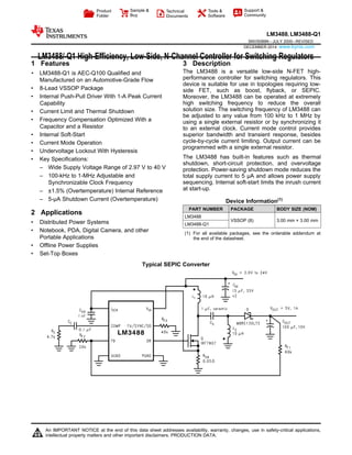
  • 1. Product Folder Sample & Buy Technical Documents Tools & Software Support & Community LM3488 LM3488-Q1, SNVS089N –JULY 2000–REVISED DECEMBER 2014 www.kynix.com LM3488/-Q1 High-Efficiency, Low-Side, N-Channel Controller for Switching Regulators 1 Features 3 Description The LM3488 is a versatile low-side N-FET high-1• LM3488-Q1 is AEC-Q100 Qualified and performance controller for switching regulators. ThisManufactured on an Automotive-Grade Flow device is suitable for use in topologies requiring low- • 8-Lead VSSOP Package side FET, such as boost, flyback, or SEPIC. • Internal Push-Pull Driver With 1-A Peak Current Moreover, the LM3488 can be operated at extremely high switching frequency to reduce the overallCapability solution size. The switching frequency of LM3488 can• Current Limit and Thermal Shutdown be adjusted to any value from 100 kHz to 1 MHz by • Frequency Compensation Optimized With a using a single external resistor or by synchronizing it Capacitor and a Resistor to an external clock. Current mode control provides • Internal Soft-Start superior bandwidth and transient response, besides cycle-by-cycle current limiting. Output current can be• Current Mode Operation programmed with a single external resistor. • Undervoltage Lockout With Hysteresis The LM3488 has built-in features such as thermal• Key Specifications: shutdown, short-circuit protection, and overvoltage – Wide Supply Voltage Range of 2.97 V to 40 V protection. Power-saving shutdown mode reduces the – 100-kHz to 1-MHz Adjustable and total supply current to 5 µA and allows power supply sequencing. Internal soft-start limits the inrush currentSynchronizable Clock Frequency at start-up.– ±1.5% (Overtemperature) Internal Reference – 5-µA Shutdown Current (Overtemperature) Device Information(1) PART NUMBER PACKAGE BODY SIZE (NOM) 2 Applications LM3488 VSSOP (8) 3.00 mm × 3.00 mm• Distributed Power Systems LM3488-Q1 • Notebook, PDA, Digital Camera, and other (1) For all available packages, see the orderable addendum at Portable Applications the end of the datasheet. • Offline Power Supplies • Set-Top Boxes Typical SEPIC Converter 1 An IMPORTANT NOTICE at the end of this data sheet addresses availability, warranty, changes, use in safety-critical applications, intellectual property matters and other important disclaimers. PRODUCTION DATA.
  • 2. LM3488, LM3488-Q1 SNVS089N –JULY 2000–REVISED DECEMBER 2014 www.ti.com Table of Contents 7.3 Feature Description................................................. 121 Features.................................................................. 1 7.4 Device Functional Modes........................................ 162 Applications ........................................................... 1 8 Application and Implementation ........................ 173 Description ............................................................. 1 8.1 Application Information............................................ 174 Revision History..................................................... 2 8.2 Typical Applications ................................................ 17 5 Pin Configuration and Functions......................... 3 9 Power Supply Recommendations...................... 286 Specifications......................................................... 3 10 Layout................................................................... 286.1 Absolute Maximum Ratings ..................................... 3 10.1 Layout Guidelines ................................................. 286.2 Handling Ratings : LM3488....................................... 4 10.2 Layout Example .................................................... 296.3 Handling Ratings: LM3488-Q1.................................. 4 11 Device and Documentation Support ................. 296.4 Recommended Operating Conditions....................... 4 11.1 Related Links ........................................................ 296.5 Thermal Information.................................................. 4 11.2 Trademarks........................................................... 306.6 Electrical Characteristics........................................... 4 11.3 Electrostatic Discharge Caution............................ 306.7 Typical Characteristics.............................................. 7 11.4 Glossary................................................................ 307 Detailed Description ............................................ 11 12 Mechanical, Packaging, and Orderable7.1 Overview ................................................................. 11 Information ........................................................... 307.2 Functional Block Diagram ....................................... 12 4 Revision History Changes from Revision M (March 2013) to Revision N Page • Added Pin Configuration and Functions section, Handling Rating table, Feature Description section, Device Functional Modes, Application and Implementation section, Power Supply Recommendations section, Layout section, Device and Documentation Support section, and Mechanical, Packaging, and Orderable Information section ................................................................................................................................................................................... 1 Changes from Revision L (March 2013) to Revision M Page • Changed layout of National Data Sheet to TI format .......................................................................................................... 29 2 Submit Documentation Feedback Copyright © 2000–2014, Texas Instruments Incorporated Product Folder Links: LM3488 LM3488-Q1
  • 3. LM3488, LM3488-Q1 www.ti.com SNVS089N –JULY 2000–REVISED DECEMBER 2014 5 Pin Configuration and Functions 8-Pin DGK VSSOP Package Top View Pin Functions PIN TYPE DESCRIPTION NAME NO. ISEN 1 I Current sense input pin. Voltage generated across an external sense resistor is fed into this pin. COMP 2 A Compensation pin. A resistor, capacitor combination connected to this pin provides compensation for the control loop. FB 3 I Feedback pin. The output voltage should be adjusted using a resistor divider to provide 1.26 V at this pin. AGND 4 P Analog ground pin. PGND 5 P Power ground pin. DR 6 O Drive pin of the IC. The gate of the external MOSFET should be connected to this pin. FA/SYNC/S 7 A Frequency adjust, synchronization, and Shutdown pin. A resistor connected to this pin sets the oscillator D frequency. An external clock signal at this pin will synchronize the controller to the frequency of the clock. A high level on this pin for ≥ 30 µs will turn the device off. The device will then draw less than 10µA from the supply. VIN 8 P Power supply input pin. 6 Specifications 6.1 Absolute Maximum Ratings (1) MIN MAX UNIT Input voltage 45 V FB pin voltage –0.4 < VFB VFB < 7 V FA/SYNC/SD pin voltage –0.4 < VFA/SYNC/SD VFA/SYNC/SD < 7 V Peak driver output current (< 10 µs) 1 A Power dissipation Internally Limited Junction temperature 150 °C Lead temperature Vapor Phase (60 s) 215 °C Infared (15 s) 260 °C DR pin voltage −0.4 ≤ VDR VDR ≤ 8 V ILIM pin voltage 600 mV (1) Absolute Maximum Ratings are limits beyond which damage to the device may occur. Recommended Operating Conditions are conditions under which operation of the device is intended to be functional. For specifications and test conditions, see the Electrical Characteristics. Copyright © 2000–2014, Texas Instruments Incorporated Submit Documentation Feedback 3 Product Folder Links: LM3488 LM3488-Q1
  • 4. LM3488, LM3488-Q1 SNVS089N –JULY 2000–REVISED DECEMBER 2014 www.ti.com 6.2 Handling Ratings : LM3488 MIN MAX UNIT Tstg Storage temperature range –65 150 °C Human body model (HBM), per ANSI/ESDA/JEDEC JS-001, all –2000 2000 pins(1) V(ESD) Electrostatic discharge V Charged device model (CDM), per JEDEC specification –750 750 JESD22-C101, all pins(2) (1) JEDEC document JEP155 states that 500-V HBM allows safe manufacturing with a standard ESD control process. (2) JEDEC document JEP157 states that 250-V CDM allows safe manufacturing with a standard ESD control process. 6.3 Handling Ratings: LM3488-Q1 MIN MAX UNIT Tstg Storage temperature range –65 150 °C Human body model (HBM), per AEC Q100-002(1) –2000 2000 Corner pins (1, 4, 5, –750 750 V(ESD) Electrostatic discharge VCharged device model (CDM), per and 8) AEC Q100-011 Other pins –750 750 (1) AEC Q100-002 indicates HBM stressing is done in accordance with the ANSI/ESDA/JEDEC JS-001 specification. 6.4 Recommended Operating Conditions MIN MAX UNIT Supply Voltage 2.97 ≤ VIN VIN ≤ 40 V Junction Temperature Range −40 ≤ TJ TJ ≤ 125 °C Switching Frequency 100 ≤ FSW FSW ≤ 1 kHz/MH z 6.5 Thermal Information LM3488, LM3488-Q1 THERMAL METRIC(1) UNIT DGK 8 PINS RθJA Junction-to-ambient thermal resistance 160 RθJC(top) Junction-to-case (top) thermal resistance 50 RθJB Junction-to-board thermal resistance 77 °C/W ψJT Junction-to-top characterization parameter 4.7 ψJB Junction-to-board characterization parameter 76 (1) For more information about traditional and new thermal metrics, see the IC Package Thermal Metrics application report, SPRA953. 6.6 Electrical Characteristics Unless otherwise specified, VIN = 12 V, RFA = 40 kΩ, TJ = 25°C PARAMETER TEST CONDITIONS MIN TYP MAX UNIT VFB Feedback Voltage VCOMP = 1.4 V, 2.97 ≤ VIN ≤ 40 V 1.2507 1.26 1.2753 V VCOMP = 1.4 V, 2.97 ≤ VIN ≤ 40 V, 1.24 1.28 −40°C ≤ TJ ≤ 125°C ΔVLINE Feedback Voltage Line Regulation 2.97 ≤ VIN ≤ 40 V 0.001 %/V ΔVLOAD Output Voltage Load Regulation IEAO Source/Sink ±0.5 %/V (max) VUVLO Input Undervoltage Lock-out 2.85 V −40°C ≤ TJ ≤ 125°C 2.97 VUV(HYS) Input Undervoltage Lock-out Hysteresis 170 mV −40°C ≤ TJ ≤ 125°C 130 210 4 Submit Documentation Feedback Copyright © 2000–2014, Texas Instruments Incorporated Product Folder Links: LM3488 LM3488-Q1
  • 5. LM3488, LM3488-Q1 www.ti.com SNVS089N –JULY 2000–REVISED DECEMBER 2014 Electrical Characteristics (continued) Unless otherwise specified, VIN = 12 V, RFA = 40 kΩ, TJ = 25°C PARAMETER TEST CONDITIONS MIN TYP MAX UNIT Fnom Nominal Switching Frequency RFA = 40 KΩ 400 kHz RFA = 40 KΩ, −40°C ≤ TJ ≤ 125°C 360 430 RDS1 (ON) Driver Switch On Resistance (top) IDR = 0.2A, VIN= 5 V 16 Ω RDS2 (ON) Driver Switch On Resistance (bottom) IDR = 0.2A 4.5 Ω VDR (max) Maximum Drive Voltage Swing(1) VIN < 7.2 V VIN V VIN ≥ 7.2 V 7.2 Dmax Maximum Duty Cycle(2) 100% Tmin (on) Minimum On Time 325 nsec −40°C ≤ TJ ≤ 125°C 230 550 ISUPPLY Supply Current (switching) See (3) 2.7 mA See (3) , −40°C ≤ TJ ≤ 125°C 3.0 IQ Quiescent Current in Shutdown Mode VFA/SYNC/SD = 5 V(4) , VIN = 5 V 5 µA VFA/SYNC/SD = 5 V(4) , VIN = 5 V, 7 −40°C ≤ TJ ≤ 125°C VSENSE Current Sense Threshold Voltage VIN = 5 V 135 156 180 mV VIN = 5 V, −40°C ≤ TJ ≤ 125°C 125 190 VSC Short-Circuit Current Limit Sense Voltage VIN = 5 V 343 mV VIN = 5 V, −40°C ≤ TJ ≤ 125°C 250 415 VSL Internal Compensation Ramp Voltage VIN = 5 V 92 mV VIN = 5 V, −40°C ≤ TJ ≤ 125°C 52 132 VSL ratio VSL/VSENSE 0.30 0.49 0.70 VOVP Output Overvoltage Protection (with VCOMP = 1.4 V 32 50 78 mV respect to feedback voltage) (5) VCOMP = 1.4 V, −40°C ≤ TJ ≤ 25 85 125°C VOVP(HYS) Output Over-Voltage Protection VCOMP = 1.4 V 60 mV Hysteresis(5) VCOMP = 1.4 V, −40°C ≤ TJ ≤ 20 110 125°C Gm Error Ampifier Transconductance VCOMP = 1.4 V, IEAO = 100 µA 600 800 1000 µmho (Source/Sink) VCOMP = 1.4 V, IEAO = 100 µA 365 1265 (Source/Sink), −40°C ≤ TJ ≤ 125°C AVOL Error Amplifier Voltage Gain VCOMP = 1.4 V, IEAO = 100 µA 38 V/V (Source/Sink) VCOMP = 1.4 V, IEAO = 100 µA 26 44 (Source/Sink), −40°C ≤ TJ ≤ 125°C IEAO Error Amplifier Output Current (Source/ Source, VCOMP = 1.4 V, VFB = 0 V 80 110 140 µA Sink) Source, VCOMP = 1.4 V, VFB = 0 V, 50 180 −40°C ≤ TJ ≤ 125°C Sink, VCOMP = 1.4 V, VFB = 1.4 V −100 −140 −180 µA Sink, VCOMP = 1.4 V, VFB = 1.4 V, −85 −185 −40°C ≤ TJ ≤ 125°C (1) The voltage on the drive pin, VDR is equal to the input voltage when input voltage is less than 7.2 V. VDR is equal to 7.2 V when the input voltage is greater than or equal to 7.2 V. (2) The limits for the maximum duty cycle can not be specified since the part does not permit less than 100% maximum duty cycle operation. (3) For this test, the FA/SYNC/SD Pin is pulled to ground using a 40K resistor . (4) For this test, the FA/SYNC/SD Pin is pulled to 5 V using a 40K resistor. (5) The over-voltage protection is specified with respect to the feedback voltage. This is because the over-voltage protection tracks the feedback voltage. The over-voltage thresold can be calculated by adding the feedback voltage, VFB to the over-voltage protection specification. Copyright © 2000–2014, Texas Instruments Incorporated Submit Documentation Feedback 5 Product Folder Links: LM3488 LM3488-Q1
  • 6. LM3488, LM3488-Q1 SNVS089N –JULY 2000–REVISED DECEMBER 2014 www.ti.com Electrical Characteristics (continued) Unless otherwise specified, VIN = 12 V, RFA = 40 kΩ, TJ = 25°C PARAMETER TEST CONDITIONS MIN TYP MAX UNIT VEAO Error Amplifier Output Voltage Swing Upper Limit: VFB = 0 V, COMP Pin 2.2 V = Floating Upper Limit: VFB = 0 V, COMP Pin 1.8 2.4 = Floating, −40°C ≤ TJ ≤ 125°C Lower Limit: VFB = 1.4 V 0.56 V Lower Limit: VFB = 1.4 V, −40°C ≤ 0.2 1.0 TJ ≤ 125°C TSS Internal Soft-Start Delay VFB = 1.2 V, VCOMP = Floating 4 ms Tr Drive Pin Rise Time Cgs = 3000 pf, VDR = 0 to 3 V 25 ns Tf Drive Pin Fall Time Cgs = 3000 pf, VDR = 0 to 3 V 25 ns VSD Shutdown and Synchronization signal Output = High 1.27 V threshold (6) Output = High, −40°C ≤ TJ ≤ 125°C 1.4 Output = Low 0.65 V Output = Low, −40°C ≤ TJ ≤ 125°C 0.3 ISD Shutdown Pin Current VSD = 5 V −1 µA VSD = 0 V +1 IFB Feedback Pin Current 15 nA TSD Thermal Shutdown 165 °C Tsh Thermal Shutdown Hysteresis 10 °C (6) The FA/SYNC/SD pin should be pulled to VIN through a resistor to turn the regulator off. 6 Submit Documentation Feedback Copyright © 2000–2014, Texas Instruments Incorporated Product Folder Links: LM3488 LM3488-Q1
  • 7. LM3488, LM3488-Q1 www.ti.com SNVS089N –JULY 2000–REVISED DECEMBER 2014 6.7 Typical Characteristics Unless otherwise specified, VIN = 12V, TJ = 25°C. Figure 1. IQ vs Temperature & Input Voltage Figure 2. ISupply vs Input Voltage (Non-Switching) Figure 3. ISupply vs VIN Figure 4. Switching Frequency vs RFA Figure 5. Frequency vs Temperature Figure 6. Drive Voltage vs Input Voltage Copyright © 2000–2014, Texas Instruments Incorporated Submit Documentation Feedback 7 Product Folder Links: LM3488 LM3488-Q1
  • 8. LM3488, LM3488-Q1 SNVS089N –JULY 2000–REVISED DECEMBER 2014 www.ti.com Typical Characteristics (continued) Unless otherwise specified, VIN = 12V, TJ = 25°C. Figure 7. Current Sense Threshold vs Input Voltage Figure 8. COMP Pin Voltage vs Load Current Figure 9. Efficiency vs Load Current (3.3 V In and 12 V Out) Figure 10. Efficiency vs Load Current (5 V In and 12 V Out) Figure 12. Efficiency vs Load Current (3.3 V In and 5 V Out)Figure 11. Efficiency vs Load Current (9 V In and 12 V Out) 8 Submit Documentation Feedback Copyright © 2000–2014, Texas Instruments Incorporated Product Folder Links: LM3488 LM3488-Q1
  • 9. LM3488, LM3488-Q1 www.ti.com SNVS089N –JULY 2000–REVISED DECEMBER 2014 Typical Characteristics (continued) Unless otherwise specified, VIN = 12V, TJ = 25°C. Figure 13. Error Amplifier Gain Figure 14. Error Amplifier Phase Figure 16. Short Circuit Protection vs Input VoltageFigure 15. COMP Pin Source Current vs Temperature Figure 18. Shutdown Threshold Hysteresis vs TemperatureFigure 17. Compensation Ramp vs Compensation Resistor Copyright © 2000–2014, Texas Instruments Incorporated Submit Documentation Feedback 9 Product Folder Links: LM3488 LM3488-Q1
  • 10. LM3488, LM3488-Q1 SNVS089N –JULY 2000–REVISED DECEMBER 2014 www.ti.com Typical Characteristics (continued) Unless otherwise specified, VIN = 12V, TJ = 25°C. Figure 19. Current Sense Voltage vs Duty Cycle 10 Submit Documentation Feedback Copyright © 2000–2014, Texas Instruments Incorporated Product Folder Links: LM3488 LM3488-Q1
  • 11. LM3488, LM3488-Q1 www.ti.com SNVS089N –JULY 2000–REVISED DECEMBER 2014 7 Detailed Description 7.1 Overview The LM3488 uses a fixed frequency, Pulse Width Modulated (PWM), current mode control architecture. In a typical application circuit, the peak current through the external MOSFET is sensed through an external sense resistor. The voltage across this resistor is fed into the ISEN pin. This voltage is then level shifted and fed into the positive input of the PWM comparator. The output voltage is also sensed through an external feedback resistor divider network and fed into the error amplifier negative input (feedback pin, FB). The output of the error amplifier (COMP pin) is added to the slope compensation ramp and fed into the negative input of the PWM comparator. At the start of any switching cycle, the oscillator sets the RS latch using the SET/Blank-out and switch logic blocks. This forces a high signal on the DR pin (gate of the external MOSFET) and the external MOSFET turns on. When the voltage on the positive input of the PWM comparator exceeds the negative input, the RS latch is reset and the external MOSFET turns off. The voltage sensed across the sense resistor generally contains spurious noise spikes, as shown in Figure 20. These spikes can force the PWM comparator to reset the RS latch prematurely. To prevent these spikes from resetting the latch, a blank-out circuit inside the IC prevents the PWM comparator from resetting the latch for a short duration after the latch is set. This duration is about 150ns and is called the blank-out time. Under extremely light load or no-load conditions, the energy delivered to the output capacitor when the external MOSFET is on during the blank-out time is more than what is delivered to the load. An over-voltage comparator inside the LM3488 prevents the output voltage from rising under these conditions. The over-voltage comparator senses the feedback (FB pin) voltage and resets the RS latch under these conditions. The latch remains in reset state till the output decays to the nominal value. Figure 20. Basic Operation of the PWM Comparator Copyright © 2000–2014, Texas Instruments Incorporated Submit Documentation Feedback 11 Product Folder Links: LM3488 LM3488-Q1
  • 12. LM3488, LM3488-Q1 SNVS089N –JULY 2000–REVISED DECEMBER 2014 www.ti.com 7.2 Functional Block Diagram 7.3 Feature Description 7.3.1 Slope Compensation Ramp The LM3488 uses a current mode control scheme. The main advantages of current mode control are inherent cycle-by-cycle current limit for the switch, and simpler control loop characteristics. It is also easy to parallel power stages using current mode control since as current sharing is automatic. Current mode control has an inherent instability for duty cycles greater than 50%, as shown in Figure 21. In Figure 21, a small increase in the load current causes the switch current to increase by ΔIO. The effect of this load change, ΔI1, is : (1) From the above equation, when D > 0.5, ΔI1 will be greater than ΔIO. In other words, the disturbance is divergent. So a very small perturbation in the load will cause the disturbance to increase. To prevent the sub-harmonic oscillations, a compensation ramp is added to the control signal, as shown in Figure 22. 12 Submit Documentation Feedback Copyright © 2000–2014, Texas Instruments Incorporated Product Folder Links: LM3488 LM3488-Q1
  • 13. MC = 40x10-6 . RSL . FS RSEN Amps second LM3488, LM3488-Q1 www.ti.com SNVS089N –JULY 2000–REVISED DECEMBER 2014 Feature Description (continued) With the compensation ramp, (2) Figure 21. Sub-Harmonic Oscillation for D0.5 Figure 22. Compensation Ramp Avoids Sub-Harmonic Oscillation The compensation ramp has been added internally in LM3488. The slope of this compensation ramp has been selected to satisfy most of the applications. The slope of the internal compensation ramp depends on the frequency. This slope can be calculated using the formula: MC = VSL.FS Volts/second (3) In the above equation, VSL is the amplitude of the internal compensation ramp. Limits for VSL have been specified in the electrical characteristics. In order to provide the user additional flexibility, a patented scheme has been implemented inside the IC to increase the slope of the compensation ramp externally, if the need arises. Adding a single external resistor, RSL(as shown in Figure 23) increases the slope of the compensation ramp, MC by : (4) In this equation, ΔVSL is equal to 40.10-6 RSL. Hence, (5) ΔVSL versus RSL has been plotted in Figure 24 for different frequencies. Copyright © 2000–2014, Texas Instruments Incorporated Submit Documentation Feedback 13 Product Folder Links: LM3488 LM3488-Q1
  • 14. LM3488, LM3488-Q1 SNVS089N –JULY 2000–REVISED DECEMBER 2014 www.ti.com Feature Description (continued) Figure 23. Increasing the Slope of the Compensation Ramp Figure 24. ΔVSL vs RSL 7.3.2 Frequency Adjust/Synchronization/Shutdown The switching frequency of LM3488 can be adjusted between 100kHz and 1MHz using a single external resistor. This resistor must be connected between FA/SYNC/SD pin and ground, as shown in Figure 25. See Typical Characteristics to determine the value of the resistor required for a desired switching frequency. The LM3488 can be synchronized to an external clock. The external clock must be connected to the FA/SYNC/SD pin through a resistor, RSYNC as shown in Figure 26. The value of this resistor is dependent on the off time of the synchronization pulse, TOFF(SYNC). Table 1 shows the range of resistors to be used for a given TOFF(SYNC). Table 1. Recommended Series Resistance for Synchronization TOFF(SYNC) (µs) RSYNC range (kΩ) 1 5 to 13 2 20 to 40 14 Submit Documentation Feedback Copyright © 2000–2014, Texas Instruments Incorporated Product Folder Links: LM3488 LM3488-Q1
  • 15. LM3488, LM3488-Q1 www.ti.com SNVS089N –JULY 2000–REVISED DECEMBER 2014 Table 1. Recommended Series Resistance for Synchronization (continued) TOFF(SYNC) (µs) RSYNC range (kΩ) 3 40 to 65 4 55 to 90 5 70 to 110 6 85 to 140 7 100 to 160 8 120 to 190 9 135 to 215 10 150 to 240 It is also necessary to have the width of the synchronization pulse wider than the duty cycle of the converter (when DR pin is high and the switching point is low). It is also necessary to have the synchronization pulse width ≥ 300nsecs. The FA/SYNC/SD pin also functions as a shutdown pin. If a high signal (see Electrical Characteristics for definition of high signal) appears on the FA/SYNC/SD pin, the LM3488 stops switching and goes into a low current mode. The total supply current of the IC reduces to less than 10µA under these conditions. Figure 27 and Figure 28 show implementation of shutdown function when operating in Frequency adjust mode and synchronization mode respectively. In frequency adjust mode, connecting the FA/SYNC/SD pin to ground forces the clock to run at a certain frequency. Pulling this pin high shuts down the IC. In frequency adjust or synchronization mode, a high signal for more than 30µs shuts down the IC. Figure 29 shows implementation of both frequency adjust with RFA resistor and frequency synchronization with RSYNC. The switching frequency is defined by RFA when a synchronization signal is not applied. When sync is applied it overrides the RFA setting. Figure 25. Frequency Adjust Figure 26. Frequency Synchronization Copyright © 2000–2014, Texas Instruments Incorporated Submit Documentation Feedback 15 Product Folder Links: LM3488 LM3488-Q1
  • 16. LM3488 FA/SYNC/SD RFA RSYNC CSYNC 270 pF LM3488, LM3488-Q1 SNVS089N –JULY 2000–REVISED DECEMBER 2014 www.ti.com Figure 27. Shutdown Operation in Frequency Adjust Mode Figure 28. Shutdown Operation in Synchronization Mode Figure 29. Frequency Adjust or Frequency Synchronization 7.3.3 Short-Circuit Protection When the voltage across the sense resistor (measured on ISEN Pin) exceeds 350mV, short-circuit current limit gets activated. A comparator inside LM3488 reduces the switching frequency by a factor of 5 and maintains this condition till the short is removed. 7.4 Device Functional Modes The device is set to run as soon as the input voltage crosses above the UVLO set point and at a frequency set according to the FA/SYNC/SD pin pull-down resistor or to run at a frequency set by the waveform applied to the FA/SYNC/SD pin. If the FA/SYNC/SD pin is pulled high, the LM3488 enters shut-down mode. If the voltage at the ISEN pin exceeds Vsc, the device enters short-circuit protection mode. 16 Submit Documentation Feedback Copyright © 2000–2014, Texas Instruments Incorporated Product Folder Links: LM3488 LM3488-Q1
  • 17. 20k RF1 CC 22 nF RC 4.7k AGND FB COMP ISEN RFA 40k VIN FA/SD/SYNC DR PGND L 10 PH 0.025: RSN Q1 IRF7807 D MBRD340 CIN 100 PF, 6.3V + VIN = 3.3V (±10%) 60k RF2 COUT 100 PF, 10V + x2 VOUT = 5V, 2A CSN 0.01 PF LM3488 LM3488, LM3488-Q1 www.ti.com SNVS089N –JULY 2000–REVISED DECEMBER 2014 8 Application and Implementation NOTE Information in the following applications sections is not part of the TI component specification, and TI does not warrant its accuracy or completeness. TI’s customers are responsible for determining suitability of components for their purposes. Customers should validate and test their design implementation to confirm system functionality. 8.1 Application Information The LM3488 may be operated in either continuous or discontinuous conduction mode. The following applications are designed for continuous conduction operation. This mode of operation has higher efficiency and lower EMI characteristics than the discontinuous mode. 8.2 Typical Applications 8.2.1 Boost Converter Figure 30. Typical High Efficiency Step-Up (Boost) Converter The most common topology for LM3488 is the boost or step-up topology. The boost converter converts a low input voltage into a higher output voltage. The basic configuration for a boost regulator is shown in Figure 31. In continuous conduction mode (when the inductor current never reaches zero at steady state), the boost regulator operates in two cycles. In the first cycle of operation, MOSFET Q is turned on and energy is stored in the inductor. During this cycle, diode D is reverse biased and load current is supplied by the output capacitor, COUT. Copyright © 2000–2014, Texas Instruments Incorporated Submit Documentation Feedback 17 Product Folder Links: LM3488 LM3488-Q1
  • 18. LM3488, LM3488-Q1 SNVS089N –JULY 2000–REVISED DECEMBER 2014 www.ti.com Typical Applications (continued) Figure 31. Simplified Boost Converter Diagram (a) First cycle of operation (b) Second cycle of operation In the second cycle, MOSFET Q is off and the diode is forward biased. The energy stored in the inductor is transferred to the load and output capacitor. The ratio of these two cycles determines the output voltage. The output voltage is defined as: (6) (ignoring the drop across the MOSFET and the diode), or where • D is the duty cycle of the switch • VD is the forward voltage drop of the diode • VQ is the drop across the MOSFET when it is on (7) 8.2.1.1 Design Requirements To calculate component values for a Boost converter, the power supply parameters shown in Table 2 should be known. The design shown in Figure 30 is the result of starting with example values shown in Table 2. Table 2. Boost Design Parameters DESIGN PARAMETER EXAMPLE VALUE Input voltage range 3V to 3.6V Output voltage 5V Maximum current 2A Operating frequency 350kHz 18 Submit Documentation Feedback Copyright © 2000–2014, Texas Instruments Incorporated Product Folder Links: LM3488 LM3488-Q1
  • 19. t (s) IL_AVG ISW_AVG D*Ts Ts D*Ts Ts IL (A) ID (A) L VIN L VV OUTIN L VV OUTIN - (a) (b) ISW (A) (C) ID_AVG =IOUT_AVG t (s) t (s) D*Ts Ts L VIN iL LM3488, LM3488-Q1 www.ti.com SNVS089N –JULY 2000–REVISED DECEMBER 2014 8.2.1.2 Detailed Design Procedure 8.2.1.2.1 Power Inductor Selection The inductor is one of the two energy storage elements in a boost converter. Figure 32 shows how the inductor current varies during a switching cycle. The current through an inductor is quantified as: (8) Figure 32. A. Inductor Current B. Diode Current C. Switch Current If VL(t) is constant, diL(t)/dt must be constant. Hence, for a given input voltage and output voltage, the current in the inductor changes at a constant rate. The important quantities in determining a proper inductance value are IL (the average inductor current) and ΔiL (the inductor current ripple). If ΔiL is larger than IL, the inductor current will drop to zero for a portion of the cycle and the converter will operate in discontinuous conduction mode. If ΔiL is smaller than IL, the inductor current will stay above zero and the converter will operate in continuous conduction mode. All the analysis in this datasheet assumes operation in continuous conduction mode. To operate in continuous conduction mode, the following conditions must be met: IL ΔiL (9) (10) (11) Copyright © 2000–2014, Texas Instruments Incorporated Submit Documentation Feedback 19 Product Folder Links: LM3488 LM3488-Q1
  • 20. DR VOUT FB L D Q ISEN COUT Rfb2 VIN LM3488 RSEN Rfb1 VOUT = 1.26(1+ RF1 RF2 ( 2fSL iL = DVIN LM3488, LM3488-Q1 SNVS089N –JULY 2000–REVISED DECEMBER 2014 www.ti.com Choose the minimum IOUT to determine the minimum L. A common choice is to set ΔiL to 30% of IL. Choosing an appropriate core size for the inductor involves calculating the average and peak currents expected through the inductor. In a boost converter, (12) and IL_peak = IL(max) + ΔiL(max), where (13) A core size with ratings higher than these values should be chosen. If the core is not properly rated, saturation will dramatically reduce overall efficiency. The LM3488 can be set to switch at very high frequencies. When the switching frequency is high, the converter can be operated with very small inductor values. With a small inductor value, the peak inductor current can be extremely higher than the output currents, especially under light load conditions. The LM3488 senses the peak current through the switch. The peak current through the switch is the same as the peak current calculated above. 8.2.1.2.2 Programming the Output Voltage The output voltage can be programmed using a resistor divider between the output and the feedback pins, as shown in Figure 33. The resistors are selected such that the voltage at the feedback pin is 1.26V. RF1 and RF2 can be selected using the equation, (14) A 100-pF capacitor may be connected between the feedback and ground pins to reduce noise. Figure 33. Adjusting the Output Voltage 20 Submit Documentation Feedback Copyright © 2000–2014, Texas Instruments Incorporated Product Folder Links: LM3488 LM3488-Q1
  • 21. RSL 40 2A RSEN x (Vo - 2VIN) 2 x fS x L - VSL RSEN 2 x VSL x fS x L Vo - (2 x VIN) RSEN = VSENSE - (D x VSENSE x VSLratio) ISWLIMIT ISWLIMIT = IOUT (1-D) + (D x VIN) (2 x fS x L) RSEN = VSENSE - (D x VSL) ISWLIMIT LM3488, LM3488-Q1 www.ti.com SNVS089N –JULY 2000–REVISED DECEMBER 2014 8.2.1.2.3 Setting the Current Limit The maximum amount of current that can be delivered to the load is set by the sense resistor, RSEN. Current limit occurs when the voltage that is generated across the sense resistor equals the current sense threshold voltage, VSENSE. When this threshold is reached, the switch will be turned off until the next cycle. Limits for VSENSE are specified in Electrical Characteristics. VSENSE represents the maximum value of the internal control signal VCS. This control signal, however, is not a constant value and changes over the course of a period as a result of the internal compensation ramp (see Figure 20). Therefore the current limit threshold will also change. The actual current limit threshold is a function of the sense voltage (VSENSE) and the internal compensation ramp: RSEN x ISWLIMIT = VCSMAX = VSENSE - (D x VSL) where • ISWLIMIT is the peak switch current limit, defined by the equation below. As duty cycle increases, the control voltage is reduced as VSL ramps up. Since current limit threshold varies with duty cycle, the following equation should be used to select RSEN and set the desired current limit threshold: (15) (16) The numerator of the above equation is VCS, and ISWLIMIT is calculated as: (17) To avoid false triggering, the current limit value should have some margin above the maximum operating value, typically 120%. Values for both VSENSE and VSL are specified in Electrical Characteristics. However, calculating with the limits of these two specs could result in an unrealistically wide current limit or RSEN range. Therefore, the following equation is recommended, using the VSL ratio value given in Electrical Characteristics: (18) RSEN is part of the current mode control loop and has some influence on control loop stability. Therefore, once the current limit threshold is set, loop stability must be verified. To verify stability, use the following equation: (19) If the selected RSEN is greater than this value, additional slope compensation must be added to ensure stability, as described in Current Limit with External Slope Compensation. 8.2.1.2.4 Current Limit with External Slope Compensation RSL is used to add additional slope compensation when required. It is not necessary in most designs and RSL should be no larger than necessary. Select RSL according to the following equation: where • RSEN is the selected value based on current limit. With RSL installed, the control signal includes additional external slope to stabilize the loop, which will also have an effect on the current limit threshold. Therefore, the current limit threshold must be re-verified, as illustrated in the equations below : (20) VCS = VSENSE – (D x (VSL + ΔVSL)) where • ΔVSL is the additional slope compensation generated and calculated as: (21) ΔVSL = 40 µA x RSL (22) Copyright © 2000–2014, Texas Instruments Incorporated Submit Documentation Feedback 21 Product Folder Links: LM3488 LM3488-Q1
  • 22. RSEN = VSENSE Vo - Vi L x fS x DISWLIMIT + ISWLIMIT = VSENSE - (D x(VSL + VSL)) RSEN LM3488, LM3488-Q1 SNVS089N –JULY 2000–REVISED DECEMBER 2014 www.ti.com This changes the equation for current limit (or RSEN) to: (23) The RSEN and RSL values may have to be calculated iteratively in order to achieve both the desired current limit and stable operation. In some designs RSL can also help to filter noise on the ISEN pin. If the inductor is selected such that ripple current is the recommended 30% value, and the current limit threshold is 120% of the maximum peak, a simpler method can be used to determine RSEN. The equation below will provide optimum stability without RSL, provided that the above 2 conditions are met: (24) 8.2.1.2.5 Power Diode Selection Observation of the boost converter circuit shows that the average current through the diode is the average load current, and the peak current through the diode is the peak current through the inductor. The diode should be rated to handle more than its peak current. The peak diode current can be calculated using the formula: ID(Peak) = IOUT/ (1−D) + ΔIL (25) In the above equation, IOUT is the output current and ΔIL has been defined in Figure 32. The peak reverse voltage for boost converter is equal to the regulator output voltage. The diode must be capable of handling this voltage. To improve efficiency, a low forward drop schottky diode is recommended. 8.2.1.2.6 Power MOSFET Selection The drive pin of LM3488 must be connected to the gate of an external MOSFET. In a boost topology, the drain of the external N-Channel MOSFET is connected to the inductor and the source is connected to the ground. The drive pin (DR) voltage depends on the input voltage (see the Typical Characteristics section). In most applications, a logic level MOSFET can be used. For very low input voltages, a sub-logic level MOSFET should be used. The selected MOSFET directly controls the efficiency. The critical parameters for selection of a MOSFET are: 1. Minimum threshold voltage, VTH(MIN) 2. On-resistance, RDS(ON) 3. Total gate charge, Qg 4. Reverse transfer capacitance, CRSS 5. Maximum drain to source voltage, VDS(MAX) The off-state voltage of the MOSFET is approximately equal to the output voltage. VDS(MAX) of the MOSFET must be greater than the output voltage. The power losses in the MOSFET can be categorized into conduction losses and ac switching or transition losses. RDS(ON) is needed to estimate the conduction losses. The conduction loss, PCOND, is the I2 R loss across the MOSFET. The maximum conduction loss is given by: where • DMAX is the maximum duty cycle. (26) (27) The turn-on and turn-off transitions of a MOSFET require times of tens of nano-seconds. CRSS and Qg are needed to estimate the large instantaneous power loss that occurs during these transitions. The amount of gate current required to turn the MOSFET on can be calculated using the formula: 22 Submit Documentation Feedback Copyright © 2000–2014, Texas Instruments Incorporated Product Folder Links: LM3488 LM3488-Q1
  • 23. VIN VIN RIN CINCBYPASSLM3488 LM3488, LM3488-Q1 www.ti.com SNVS089N –JULY 2000–REVISED DECEMBER 2014 IG = Qg.FS (28) The required gate drive power to turn the MOSFET on is equal to the switching frequency times the energy required to deliver the charge to bring the gate charge voltage to VDR (see the Electrical Characteristics table and the Typical Characteristics section for the drive voltage specification). PDrive = FS.Qg.VDR (29) 8.2.1.2.7 Input Capacitor Selection Due to the presence of an inductor at the input of a boost converter, the input current waveform is continuous and triangular, as shown in Figure 32. The inductor ensures that the input capacitor sees fairly low ripple currents. However, as the input capacitor gets smaller, the input ripple goes up. The rms current in the input capacitor is given by: (30) The input capacitor should be capable of handling the rms current. Although the input capacitor is not as critical in a boost application, low values can cause impedance interactions. Therefore a good quality capacitor should be chosen in the range of 10 µF to 20 µF. If a value lower than 10µF is used, then problems with impedance interactions or switching noise can affect the LM3488. To improve performance, especially with VIN below 8 volts, it is recommended to use a 20Ω resistor at the input to provide a RC filter. The resistor is placed in series with the VIN pin with only a bypass capacitor attached to the VIN pin directly (see Figure 34). A 0.1-µF or 1-µF ceramic capacitor is necessary in this configuration. The bulk input capacitor and inductor will connect on the other side of the resistor with the input power supply. Figure 34. Reducing IC Input Noise 8.2.1.2.8 Output Capacitor Selection The output capacitor in a boost converter provides all the output current when the inductor is charging. As a result it sees very large ripple currents. The output capacitor should be capable of handling the maximum rms current. The rms current in the output capacitor is: (31) Where (32) and D, the duty cycle is equal to (VOUT − VIN)/VOUT. The ESR and ESL of the output capacitor directly control the output ripple. Use capacitors with low ESR and ESL at the output for high efficiency and low ripple voltage. Surface Mount tantalums, surface mount polymer electrolytic and polymer tantalum, Sanyo- OSCON, or multi-layer ceramic capacitors are recommended at the output. Copyright © 2000–2014, Texas Instruments Incorporated Submit Documentation Feedback 23 Product Folder Links: LM3488 LM3488-Q1
  • 24. LM3488, LM3488-Q1 SNVS089N –JULY 2000–REVISED DECEMBER 2014 www.ti.com 8.2.1.3 Application Curve Figure 35. Typical Startup Waveform (horizontal scale: 10ms/DIV) 8.2.2 Designing SEPIC Using LM3488 Since the LM3488 controls a low-side N-Channel MOSFET, it can also be used in SEPIC (Single Ended Primary Inductance Converter) applications. An example of SEPIC using LM3488 is shown in Figure 36. As shown in Figure 36, the output voltage can be higher or lower than the input voltage. The SEPIC uses two inductors to step-up or step-down the input voltage. The inductors L1 and L2 can be two discrete inductors or two windings of a coupled transformer since equal voltages are applied across the inductor throughout the switching cycle. Using two discrete inductors allows use of catalog magnetics, as opposed to a custom transformer. The input ripple can be reduced along with size by using the coupled windings of transformer for L1 and L2. Figure 36. Typical SEPIC Converter Due to the presence of the inductor L1 at the input, the SEPIC inherits all the benefits of a boost converter. One main advantage of SEPIC over boost converter is the inherent input to output isolation. The capacitor CS isolates the input from the output and provides protection against shorted or malfunctioning load. Hence, the A SEPIC is useful for replacing boost circuits when true shutdown is required. This means that the output voltage falls to 0V when the switch is turned off. In a boost converter, the output can only fall to the input voltage minus a diode drop. 24 Submit Documentation Feedback Copyright © 2000–2014, Texas Instruments Incorporated Product Folder Links: LM3488 LM3488-Q1
  • 25. LM3488, LM3488-Q1 www.ti.com SNVS089N –JULY 2000–REVISED DECEMBER 2014 The duty cycle of a SEPIC is given by: (33) In the above equation, VQ is the on-state voltage of the MOSFET, Q, and VDIODE is the forward voltage drop of the diode. 8.2.2.1 Design Requirements To calculate component values for a SEPIC converter, the power supply parameters shown in Table 3 should be known. The design shown in Figure 36 is the result of starting with example values shown in Table 3 Table 3. SEPIC Design Parameters DESIGN PARAMETER EXAMPLE VALUE Input voltage range 3 V to 24 V Output voltage 5 V Maximum current 1 A Operating frequency 350 kHz Max peak to peak output ripple 200 mV 8.2.2.2 Detailed Design Procedure 8.2.2.2.1 Power MOSFET Selection As in boost converter, the parameters governing the selection of the MOSFET are the minimum threshold voltage, VTH(MIN), the on-resistance, RDS(ON), the total gate charge, Qg, the reverse transfer capacitance, CRSS, and the maximum drain to source voltage, VDS(MAX). The peak switch voltage in a SEPIC is given by: VSW(PEAK) = VIN + VOUT + VDIODE (34) The selected MOSFET should satisfy the condition: VDS(MAX) VSW(PEAK) (35) The peak switch current is given by: (36) The rms current through the switch is given by: (37) 8.2.2.2.2 Power Diode Selection The Power diode must be selected to handle the peak current and the peak reverse voltage. In a SEPIC, the diode peak current is the same as the switch peak current. The off-state voltage or peak reverse voltage of the diode is VIN + VOUT. Similar to the boost converter, the average diode current is equal to the output current. Schottky diodes are recommended. 8.2.2.2.3 Selection Of Inductors L1 and L2 Proper selection of the inductors L1 and L2 to maintain constant current mode requires calculations of the following parameters. Average current in the inductors: (38) IL2AVE = IOUT (39) Copyright © 2000–2014, Texas Instruments Incorporated Submit Documentation Feedback 25 Product Folder Links: LM3488 LM3488-Q1
  • 26. RSEN = VSENSE - D(VSL + VSL) ISWPEAK 2 VOUT = IOUT 1-D + IL2 ( ) ESR L2 (VIN - VQ)D 2IOUTfS L1 (VIN - VQ)(1-D) 2IOUTfS LM3488, LM3488-Q1 SNVS089N –JULY 2000–REVISED DECEMBER 2014 www.ti.com Peak to peak ripple current, to calculate core loss if necessary: (40) (41) maintains the condition IL ΔiL/2 to ensure constant current mode. (42) (43) Peak current in the inductor, to ensure the inductor does not saturate: (44) (45) IL1PK must be lower than the maximum current rating set by the current sense resistor. The value of L1 can be increased above the minimum recommended to reduce input ripple and output ripple. However, once DIL1 is less than 20% of IL1AVE, the benefit to output ripple is minimal. By increasing the value of L2 above the minimum recommended, ΔIL2 can be reduced, which in turn will reduce the output ripple voltage: where • ESR is the effective series resistance of the output capacitor. (46) If L1 and L2 are wound on the same core, then L1 = L2 = L. All the equations above will hold true if the inductance is replaced by 2L. A good choice for transformer with equal turns is Coiltronics CTX series Octopack. 8.2.2.2.4 Sense Resistor Selection The peak current through the switch, ISW(PEAK) can be adjusted using the current sense resistor, RSEN, to provide a certain output current. Resistor RSEN can be selected using the formula: (47) 8.2.2.2.5 SEPIC Capacitor Selection The selection of SEPIC capacitor, CS, depends on the rms current. The rms current of the SEPIC capacitor is given by: (48) 26 Submit Documentation Feedback Copyright © 2000–2014, Texas Instruments Incorporated Product Folder Links: LM3488 LM3488-Q1
  • 27. IRMS = ISWPK 2 - ISWPK (IL1 + IL2)+ (IL1 + IL2)2 3 (1-D) - IOUT 2 LM3488, LM3488-Q1 www.ti.com SNVS089N –JULY 2000–REVISED DECEMBER 2014 The SEPIC capacitor must be rated for a large ACrms current relative to the output power. This property makes the SEPIC much better suited to lower power applications where the rms current through the capacitor is relatively small (relative to capacitor technology). The voltage rating of the SEPIC capacitor must be greater than the maximum input voltage. Tantalum capacitors are the best choice for SMT, having high rms current ratings relative to size. Ceramic capacitors could be used, but the low C values will tend to cause larger changes in voltage across the capacitor due to the large currents. High C value ceramics are expensive. Electrolytics work well for through hole applications where the size required to meet the rms current rating can be accommodated. There is an energy balance between CS and L1, which can be used to determine the value of the capacitor. The basic energy balance equation is: (49) Where (50) is the ripple voltage across the SEPIC capacitor, and (51) is the ripple current through the inductor L1. The energy balance equation can be solved to provide a minimum value for CS: (52) 8.2.2.2.6 Input Capacitor Selection Similar to a boost converter, the SEPIC has an inductor at the input. Hence, the input current waveform is continuous and triangular. The inductor ensures that the input capacitor sees fairly low ripple currents. However, as the input capacitor gets smaller, the input ripple goes up. The rms current in the input capacitor is given by: (53) The input capacitor should be capable of handling the rms current. Although the input capacitor is not as critical in a boost application, low values can cause impedance interactions. Therefore a good quality capacitor should be chosen in the range of 10µF to 20µF. If a value lower than 10µF is used, then problems with impedance interactions or switching noise can affect the LM3488. To improve performance, especially with VIN below 8 volts, it is recommended to use a 20Ω resistor at the input to provide a RC filter. The resistor is placed in series with the VIN pin with only a bypass capacitor attached to the VIN pin directly (see Figure 34). A 0.1µF or 1µF ceramic capacitor is necessary in this configuration. The bulk input capacitor and inductor will connect on the other side of the resistor with the input power supply. 8.2.2.2.7 Output Capacitor Selection The ESR and ESL of the output capacitor directly control the output ripple. Use low capacitors with low ESR and ESL at the output for high efficiency and low ripple voltage. Surface mount tantalums, surface mount polymer electrolytic and polymer tantalum, Sanyo- OSCON, or multi-layer ceramic capacitors are recommended at the output. The output capacitor of the SEPIC sees very large ripple currents (similar to the output capacitor of a boost converter. The rms current through the output capacitor is given by: (54) Copyright © 2000–2014, Texas Instruments Incorporated Submit Documentation Feedback 27 Product Folder Links: LM3488 LM3488-Q1
  • 28. LM3488, LM3488-Q1 SNVS089N –JULY 2000–REVISED DECEMBER 2014 www.ti.com The ESR and ESL of the output capacitor directly control the output ripple. Use low capacitors with low ESR and ESL at the output for high efficiency and low ripple voltage. Surface mount tantalums, surface mount polymer electrolytic and polymer tantalum, Sanyo- OSCON, or multi-layer ceramic capacitors are recommended at the output for low ripple. 9 Power Supply Recommendations The LM3488 is designed to operate from various DC power supply including a car battery. If so, VIN input should be protected from reversal voltage and voltage dump over 48 Volts. The impedance of the input supply rail should be low enough that the input current transient does not cause drop below VIN UVLO level. If the input supply is connected by using long wires, additional bulk capacitance may be required in addition to normal input capacitor. 10 Layout 10.1 Layout Guidelines Good board layout is critical for switching controllers such as the LM3488. First the ground plane area must be sufficient for thermal dissipation purposes and second, appropriate guidelines must be followed to reduce the effects of switching noise. Switch mode converters are very fast switching devices. In such devices, the rapid increase of input current combined with the parasitic trace inductance generates unwanted Ldi/dt noise spikes. The magnitude of this noise tends to increase as the output current increases. This parasitic spike noise may turn into electromagnetic interference (EMI), and can also cause problems in device performance. Therefore, care must be taken in layout to minimize the effect of this switching noise. The current sensing circuit in current mode devices can be easily effected by switching noise. This noise can cause duty cycle jitter which leads to increased spectral noise. The most important layout rule is to keep the AC current loops as small as possible. Figure 37 shows the current flow of a boost converter. The top schematic shows a dotted line which represents the current flow during onstate and the middle schematic shows the current flow during off-state. The bottom schematic shows the currents we refer to as AC currents. They are the most critical ones since current is changing in very short time periods. The dotted lined traces of the bottom schematic are the once to make as short as possible. Figure 37. Current Flow in a Boost Application 28 Submit Documentation Feedback Copyright © 2000–2014, Texas Instruments Incorporated Product Folder Links: LM3488 LM3488-Q1
  • 29. Sense Resistor Gate Resistor Tune Performance Output Diode Power FET Output Inductor Set Frequency Set Output Voltage Compensation Chip Power Filter Current Sense Filter To Input Shutdown To Output AGND PGND FB COMP ISEN DR To DR Pin Output Capacitors Input Capacitors Current sense trace changes layers to allow continuous ground plane LM3488 FA/SYNC/SD VIN LM3488, LM3488-Q1 www.ti.com SNVS089N –JULY 2000–REVISED DECEMBER 2014 Layout Guidelines (continued) The PGND and AGND pins have to be connected to the same ground very close to the IC. To avoid ground loop currents attach all the grounds of the system only at one point. A ceramic input capacitor should be connected as close as possible to the Vin pin and grounded close to the GND pin. For a layout example please see AN-1204 LM378/LM3488 Evaluation Board (SNVA656A). For more information about layout in switch mode power supplies please refer to AN-1229 SIMPLE SWITCHER® PCB Layout Guidelines (SNVA054c). 10.2 Layout Example Figure 38. Example Layout of a Boost Application using LM3488 11 Device and Documentation Support 11.1 Related Links The table below lists quick access links. Categories include technical documents, support and community resources, tools and software, and quick access to sample or buy. Table 4. Related Links TECHNICAL TOOLS SUPPORT PARTS PRODUCT FOLDER SAMPLE BUY DOCUMENTS SOFTWARE COMMUNITY LM3488 Click here Click here Click here Click here Click here LM3488-Q1 Click here Click here Click here Click here Click here Copyright © 2000–2014, Texas Instruments Incorporated Submit Documentation Feedback 29 Product Folder Links: LM3488 LM3488-Q1
  • 30. LM3488, LM3488-Q1 SNVS089N –JULY 2000–REVISED DECEMBER 2014 www.ti.com 11.2 Trademarks All trademarks are the property of their respective owners. 11.3 Electrostatic Discharge Caution These devices have limited built-in ESD protection. The leads should be shorted together or the device placed in conductive foam during storage or handling to prevent electrostatic damage to the MOS gates. 11.4 Glossary SLYZ022 — TI Glossary. This glossary lists and explains terms, acronyms, and definitions. 12 Mechanical, Packaging, and Orderable Information The following pages include mechanical, packaging, and orderable information. This information is the most current data available for the designated devices. This data is subject to change without notice and revision of this document. For browser-based versions of this data sheet, refer to the left-hand navigation. 30 Submit Documentation Feedback Copyright © 2000–2014, Texas Instruments Incorporated Product Folder Links: LM3488 LM3488-Q1
  • 31. PACKAGE OPTION ADDENDUM www.ti.com 1-Nov-2015 Addendum-Page 1 PACKAGING INFORMATION Orderable Device Status (1) Package Type Package Drawing Pins Package Qty Eco Plan (2) Lead/Ball Finish (6) MSL Peak Temp (3) Op Temp (°C) Device Marking (4/5) Samples LM3488MM ACTIVE VSSOP DGK 8 1000 TBD Call TI Call TI S21B LM3488MM/NOPB ACTIVE VSSOP DGK 8 1000 Green (RoHS no Sb/Br) CU NIPDAUAG | CU SN Level-1-260C-UNLIM -40 to 125 S21B LM3488MMX NRND VSSOP DGK 8 TBD Call TI Call TI -40 to 125 S21B LM3488MMX/NOPB ACTIVE VSSOP DGK 8 3500 Green (RoHS no Sb/Br) CU NIPDAUAG | CU SN Level-1-260C-UNLIM -40 to 125 S21B LM3488QMM/NOPB ACTIVE VSSOP DGK 8 1000 Green (RoHS no Sb/Br) CU SN Level-1-260C-UNLIM -40 to 125 SSKB LM3488QMMX/NOPB ACTIVE VSSOP DGK 8 3500 Green (RoHS no Sb/Br) CU SN Level-1-260C-UNLIM -40 to 125 SSKB (1) The marketing status values are defined as follows: ACTIVE: Product device recommended for new designs. LIFEBUY: TI has announced that the device will be discontinued, and a lifetime-buy period is in effect. NRND: Not recommended for new designs. Device is in production to support existing customers, but TI does not recommend using this part in a new design. PREVIEW: Device has been announced but is not in production. Samples may or may not be available. OBSOLETE: TI has discontinued the production of the device. (2) Eco Plan - The planned eco-friendly classification: Pb-Free (RoHS), Pb-Free (RoHS Exempt), or Green (RoHS no Sb/Br) - please check http://www.ti.com/productcontent for the latest availability information and additional product content details. TBD: The Pb-Free/Green conversion plan has not been defined. Pb-Free (RoHS): TI's terms Lead-Free or Pb-Free mean semiconductor products that are compatible with the current RoHS requirements for all 6 substances, including the requirement that lead not exceed 0.1% by weight in homogeneous materials. Where designed to be soldered at high temperatures, TI Pb-Free products are suitable for use in specified lead-free processes. Pb-Free (RoHS Exempt): This component has a RoHS exemption for either 1) lead-based flip-chip solder bumps used between the die and package, or 2) lead-based die adhesive used between the die and leadframe. The component is otherwise considered Pb-Free (RoHS compatible) as defined above. Green (RoHS no Sb/Br): TI defines Green to mean Pb-Free (RoHS compatible), and free of Bromine (Br) and Antimony (Sb) based flame retardants (Br or Sb do not exceed 0.1% by weight in homogeneous material) (3) MSL, Peak Temp. - The Moisture Sensitivity Level rating according to the JEDEC industry standard classifications, and peak solder temperature. (4) There may be additional marking, which relates to the logo, the lot trace code information, or the environmental category on the device. (5) Multiple Device Markings will be inside parentheses. Only one Device Marking contained in parentheses and separated by a ~ will appear on a device. If a line is indented then it is a continuation of the previous line and the two combined represent the entire Device Marking for that device.
  • 32. PACKAGE OPTION ADDENDUM www.ti.com 1-Nov-2015 Addendum-Page 2 (6) Lead/Ball Finish - Orderable Devices may have multiple material finish options. Finish options are separated by a vertical ruled line. Lead/Ball Finish values may wrap to two lines if the finish value exceeds the maximum column width. Important Information and Disclaimer:The information provided on this page represents TI's knowledge and belief as of the date that it is provided. TI bases its knowledge and belief on information provided by third parties, and makes no representation or warranty as to the accuracy of such information. Efforts are underway to better integrate information from third parties. TI has taken and continues to take reasonable steps to provide representative and accurate information but may not have conducted destructive testing or chemical analysis on incoming materials and chemicals. TI and TI suppliers consider certain information to be proprietary, and thus CAS numbers and other limited information may not be available for release. In no event shall TI's liability arising out of such information exceed the total purchase price of the TI part(s) at issue in this document sold by TI to Customer on an annual basis.
  • 33. TAPE AND REEL INFORMATION *All dimensions are nominal Device Package Type Package Drawing Pins SPQ Reel Diameter (mm) Reel Width W1 (mm) A0 (mm) B0 (mm) K0 (mm) P1 (mm) W (mm) Pin1 Quadrant LM3488MM VSSOP DGK 8 1000 178.0 12.4 5.3 3.4 1.4 8.0 12.0 Q1 LM3488MM/NOPB VSSOP DGK 8 1000 178.0 12.4 5.3 3.4 1.4 8.0 12.0 Q1 LM3488MMX/NOPB VSSOP DGK 8 3500 330.0 12.4 5.3 3.4 1.4 8.0 12.0 Q1 LM3488QMM/NOPB VSSOP DGK 8 1000 178.0 12.4 5.3 3.4 1.4 8.0 12.0 Q1 LM3488QMMX/NOPB VSSOP DGK 8 3500 330.0 12.4 5.3 3.4 1.4 8.0 12.0 Q1 PACKAGE MATERIALS INFORMATION www.ti.com 2-Sep-2015 Pack Materials-Page 1
  • 34. *All dimensions are nominal Device Package Type Package Drawing Pins SPQ Length (mm) Width (mm) Height (mm) LM3488MM VSSOP DGK 8 1000 210.0 185.0 35.0 LM3488MM/NOPB VSSOP DGK 8 1000 210.0 185.0 35.0 LM3488MMX/NOPB VSSOP DGK 8 3500 367.0 367.0 35.0 LM3488QMM/NOPB VSSOP DGK 8 1000 210.0 185.0 35.0 LM3488QMMX/NOPB VSSOP DGK 8 3500 367.0 367.0 35.0 PACKAGE MATERIALS INFORMATION www.ti.com 2-Sep-2015 Pack Materials-Page 2
  • 35.
  • 36.
  • 37. IMPORTANT NOTICE Texas Instruments Incorporated and its subsidiaries (TI) reserve the right to make corrections, enhancements, improvements and other changes to its semiconductor products and services per JESD46, latest issue, and to discontinue any product or service per JESD48, latest issue. Buyers should obtain the latest relevant information before placing orders and should verify that such information is current and complete. All semiconductor products (also referred to herein as “components”) are sold subject to TI’s terms and conditions of sale supplied at the time of order acknowledgment. TI warrants performance of its components to the specifications applicable at the time of sale, in accordance with the warranty in TI’s terms and conditions of sale of semiconductor products. Testing and other quality control techniques are used to the extent TI deems necessary to support this warranty. Except where mandated by applicable law, testing of all parameters of each component is not necessarily performed. TI assumes no liability for applications assistance or the design of Buyers’ products. Buyers are responsible for their products and applications using TI components. To minimize the risks associated with Buyers’ products and applications, Buyers should provide adequate design and operating safeguards. TI does not warrant or represent that any license, either express or implied, is granted under any patent right, copyright, mask work right, or other intellectual property right relating to any combination, machine, or process in which TI components or services are used. Information published by TI regarding third-party products or services does not constitute a license to use such products or services or a warranty or endorsement thereof. Use of such information may require a license from a third party under the patents or other intellectual property of the third party, or a license from TI under the patents or other intellectual property of TI. Reproduction of significant portions of TI information in TI data books or data sheets is permissible only if reproduction is without alteration and is accompanied by all associated warranties, conditions, limitations, and notices. TI is not responsible or liable for such altered documentation. Information of third parties may be subject to additional restrictions. Resale of TI components or services with statements different from or beyond the parameters stated by TI for that component or service voids all express and any implied warranties for the associated TI component or service and is an unfair and deceptive business practice. TI is not responsible or liable for any such statements. Buyer acknowledges and agrees that it is solely responsible for compliance with all legal, regulatory and safety-related requirements concerning its products, and any use of TI components in its applications, notwithstanding any applications-related information or support that may be provided by TI. Buyer represents and agrees that it has all the necessary expertise to create and implement safeguards which anticipate dangerous consequences of failures, monitor failures and their consequences, lessen the likelihood of failures that might cause harm and take appropriate remedial actions. Buyer will fully indemnify TI and its representatives against any damages arising out of the use of any TI components in safety-critical applications. In some cases, TI components may be promoted specifically to facilitate safety-related applications. With such components, TI’s goal is to help enable customers to design and create their own end-product solutions that meet applicable functional safety standards and requirements. Nonetheless, such components are subject to these terms. No TI components are authorized for use in FDA Class III (or similar life-critical medical equipment) unless authorized officers of the parties have executed a special agreement specifically governing such use. Only those TI components which TI has specifically designated as military grade or “enhanced plastic” are designed and intended for use in military/aerospace applications or environments. Buyer acknowledges and agrees that any military or aerospace use of TI components which have not been so designated is solely at the Buyer's risk, and that Buyer is solely responsible for compliance with all legal and regulatory requirements in connection with such use. TI has specifically designated certain components as meeting ISO/TS16949 requirements, mainly for automotive use. In any case of use of non-designated products, TI will not be responsible for any failure to meet ISO/TS16949. Products Applications Audio www.ti.com/audio Automotive and Transportation www.ti.com/automotive Amplifiers amplifier.ti.com Communications and Telecom www.ti.com/communications Data Converters dataconverter.ti.com Computers and Peripherals www.ti.com/computers DLP® Products www.dlp.com Consumer Electronics www.ti.com/consumer-apps DSP dsp.ti.com Energy and Lighting www.ti.com/energy Clocks and Timers www.ti.com/clocks Industrial www.ti.com/industrial Interface interface.ti.com Medical www.ti.com/medical Logic logic.ti.com Security www.ti.com/security Power Mgmt power.ti.com Space, Avionics and Defense www.ti.com/space-avionics-defense Microcontrollers microcontroller.ti.com Video and Imaging www.ti.com/video RFID www.ti-rfid.com OMAP Applications Processors www.ti.com/omap TI E2E Community e2e.ti.com Wireless Connectivity www.ti.com/wirelessconnectivity Mailing Address: Texas Instruments, Post Office Box 655303, Dallas, Texas 75265 Copyright © 2015, Texas Instruments Incorporated http://www.kynix.com/Search/LM3488.html