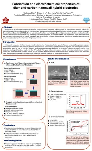
1. A. Fabrication of CNWs-on-diamond and CNWs-on-
silicon as Electrochemical Electrodes
Polycrystalline diamond
DC-PECVD
500 ℃ ~ 900℃
CH4 of 2% was diluted by H2
Carbon nanowalls
DC-PECVD
800 ℃ ~ 900℃
CH4 of 8% was diluted by H2
Fabrication and electrochemical properties of
diamond-carbon-nanowall hybrid electrodes
Waileong Chen1, Chiuan-Yi Li2, Shin-Hung Yei1, Yonhua Tzeng1,2
1Institute of Microelectronics, 2Institute of Nanotechnology and Microsystems Engineering
National Cheng Kung University
1, University Road, Tainan City 701, Taiwan, ROC
Email:tzengyo@mail.ncku.edu.tw
Conclusions
Acknowledgement
We report an all carbon electrochemical electrode based on carbon nanowalls (CNWs) grown on polycrystalline diamond (CNWs-on-
diamond) for electrochemical applications. This micro-nano diamond-nanowall structure was fabricated by Direct Current Plasma Enhanced
Chemical Vapor Deposition (DC-PECVD) in a gas mixture of methane and hydrogen. Diamond possesses excellent chemical inertness for
corrosive electrochemical applications. By combining outstanding properties of diamond and the high-aspect ratio, large effective surface
and high electrical conductivity of carbon nanowalls, we demonstrated a hybrid electrochemical electrode of excellent electrochemical
performance based on cyclic voltammetry (CV) measurements.
We observed lower background current and lager potential
window for CNWs-on-diamond electrodes than CNWs-on-
silicon electrodes.
CNWs-on-diamond is a much better hybrid material for
electrochemical applications than CNWs-on-silicon
electrodes.
In this work, we used a thin layer of poly-crystalline diamond as the substrate for the growth of carbon nanowalls for applications as an
electrochemical electrode. The underlying diamond film protects the silicon surface, on which diamond is grown, from reacting with corrosive
environments such as that in a H2S04 solution. CNW structure has been examined by Scanning Electron Microscopy (SEM). The
electrochemical signal has been studied by the CV method. The cyclic voltammetric curves provide information about electron transfer
kinetics and thermodynamics. From the signals, we can know the chemical reactions which happen on the electrode surface. We anticipate
these diamond-carbon nanowall hybrid electrodes to be good electrode materials for biosensor applications.
Financial support by NSC Taiwan under the grants NSC-98-
3114-M-006-001& NSC-96-2221-E-006-286-MY3 is highly
appreciated.
Diamond & Devices Lab
B. Analysis of Surface Structure and Electrochemical
Measurements
Cyclic voltammetry
Three electrode cells system
Ag/AgCl reference electrode
At room temperature
0.1M H2SO4 aqueous solutions
The scan rate was 50mV/s
-2 -1 0 1 2
-12
-8
-4
0
4
8
12
CurrentDensity(mA/cm2
)
Potential vs Ag/AgCl (Voltage)
CNWs-on-diamond
CNWs-on-silicon
Fig.4. CV curves of a CNWs-on-
diamond electrode (black line) and a
CNWs-on-silicon (red line) electrode
measured in 0.1 M H2SO4 aqueous
solutions. The scan rate was 50mV/s.
A. SEM
C. CV measurements
Fig.2. SEM images of the top
view of CNWs-on-diamond
( the inset shows the zoom-in
carbon nanowalls)
Abstract
Introduction
Experimental Results and Discussion
B. Raman Spectrum
Fig.1. SEM image of cross-
sectional view of CNWs-on-
diamond
Fig.3. Raman spectrum of CNWs-
on-diamond
1000 1200 1400 1600 1800
20
40
60
80
100
120
140
Intensity(a.u.)
Raman shift (cm-1)
CNWs-on-diamond
D band
G band
Laser excitation = 532 nm
G band = 1580 cm-1
D band = 1350 cm-1
IG/ID ~ 2.0
Silicon substrate
Si wafer
Diamond Seeding
Polycrystalline diamond
deposition
Carbon nanowalls
on diamond
0.1 M H2SO4
Scan rate was 50mV/s
Scan range = -2.5V~2V
Surface area = 0.071cm2
(1)
(2)
(3)(4)