Study of V-ICharacteristics of PN
Junction Diode
Experiment - 9
Department of Electrical &
Electronics Engineering
2.
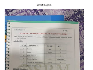
Aim
• To studythe Volt-Ampere Characteristics of
Silicon P-N Junction Diode in forward and
reverse bias conditions.
3.
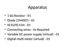
Apparatus
• 1 kΩResistor - 01
• Diode (1N4007) - 01
• NI ELVIS II kit - 01
• Connecting wires - As Required
• Variable DC power supply (virtual) - 01
• Digital multi meter (virtual) - 01
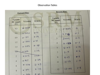
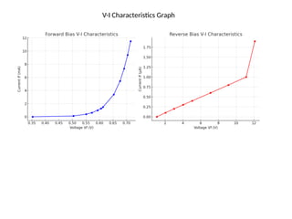
Conclusion
• • Inforward bias, the current increases
exponentially with voltage after the threshold
(around 0.6V).
• • In reverse bias, the current remains very low,
indicating negligible conduction.
• • This behavior verifies the typical
characteristics of a silicon PN junction diode.