This document discusses bipolar junction transistors (BJTs) and field effect transistors (FETs). It provides information on:
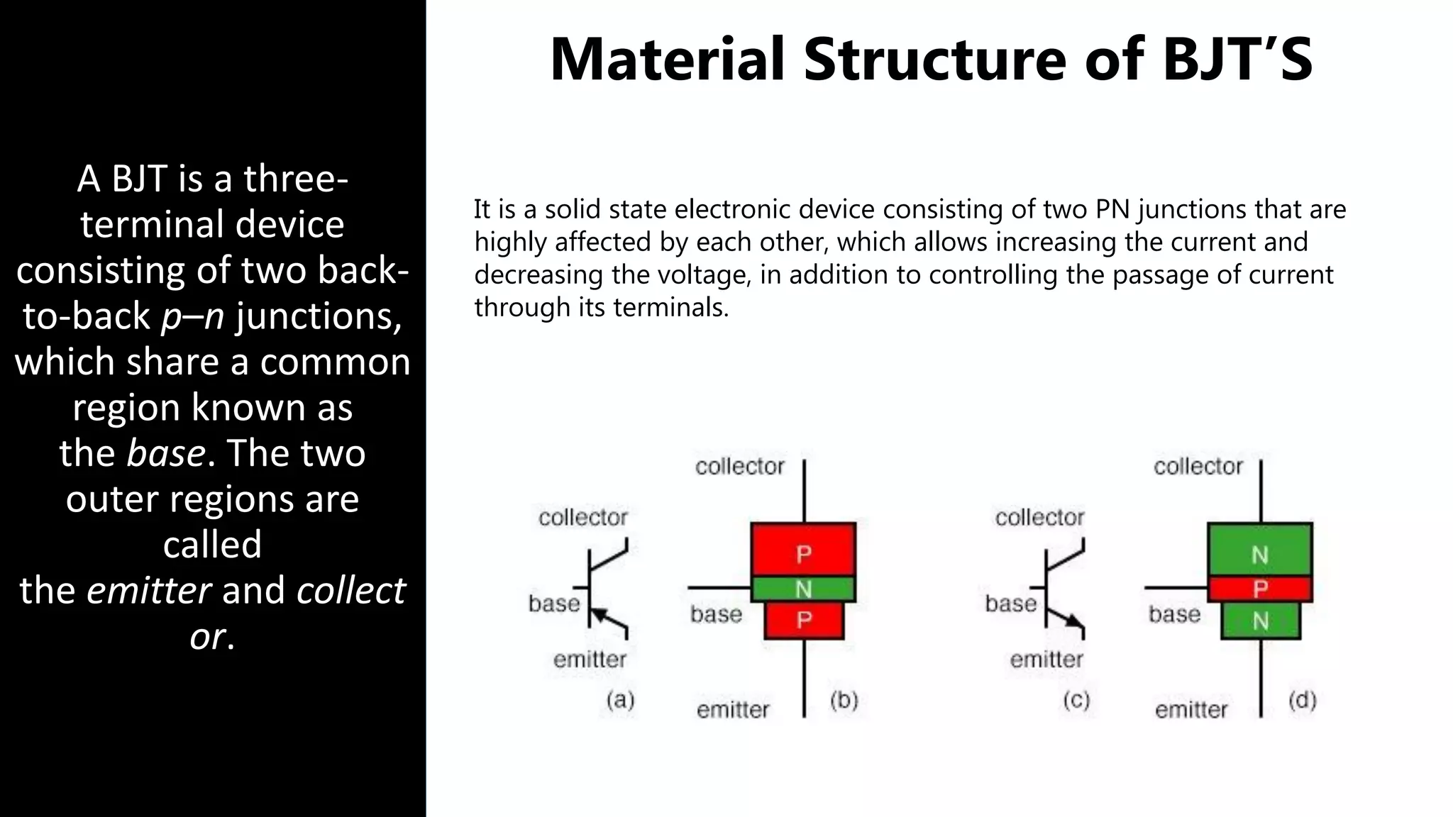
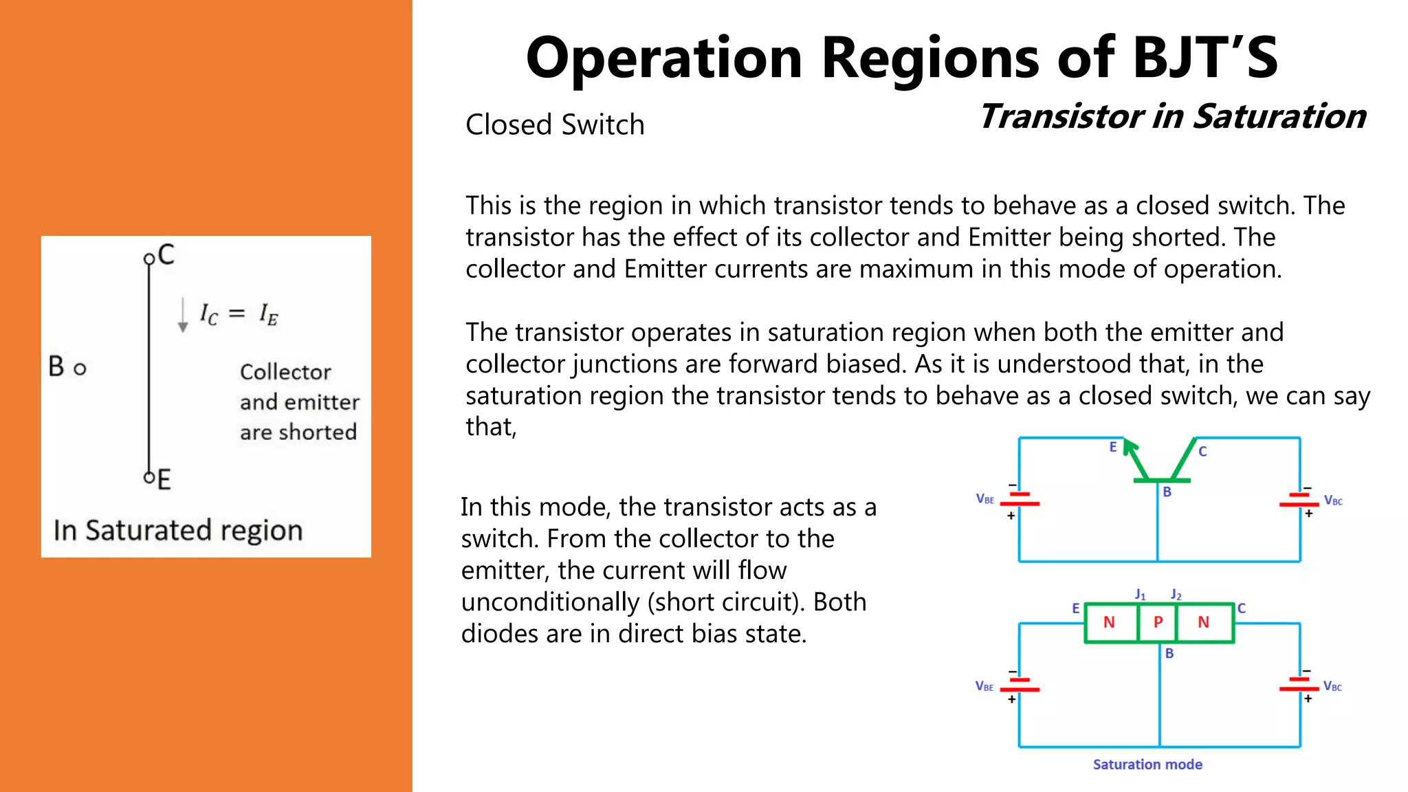
1. The material structure and operation regions of BJTs, including active, cutoff, and saturation regions where the transistor acts as an amplifier, open switch, and closed switch respectively.
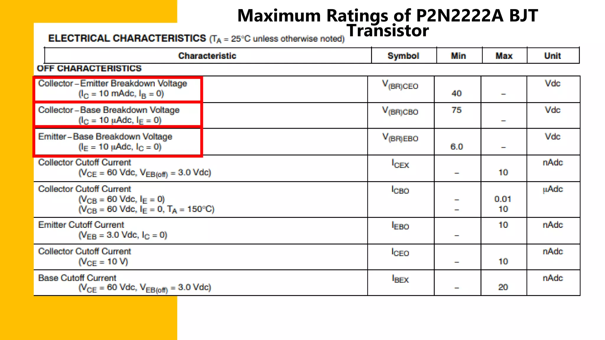
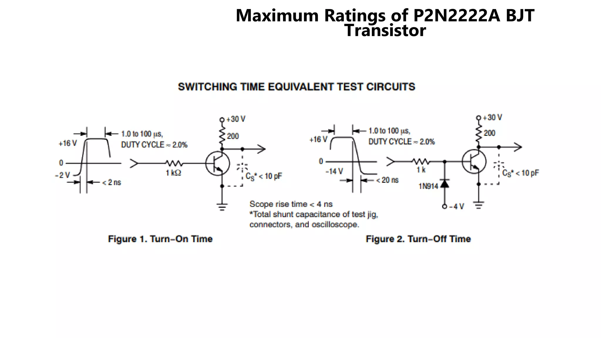
2. Maximum ratings for the P2N2222A BJT transistor.
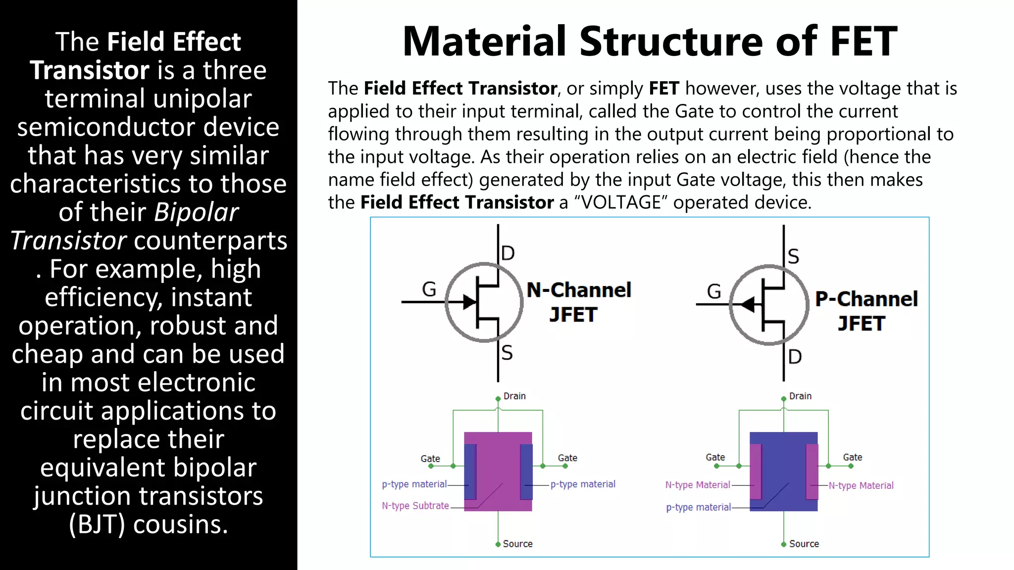
3. The material structure of FETs which use a gate voltage to control current flow, making them voltage-operated devices.
4. The operation regions of FETs including cutoff, ohmic/linear, and saturation regions and descriptions of each.
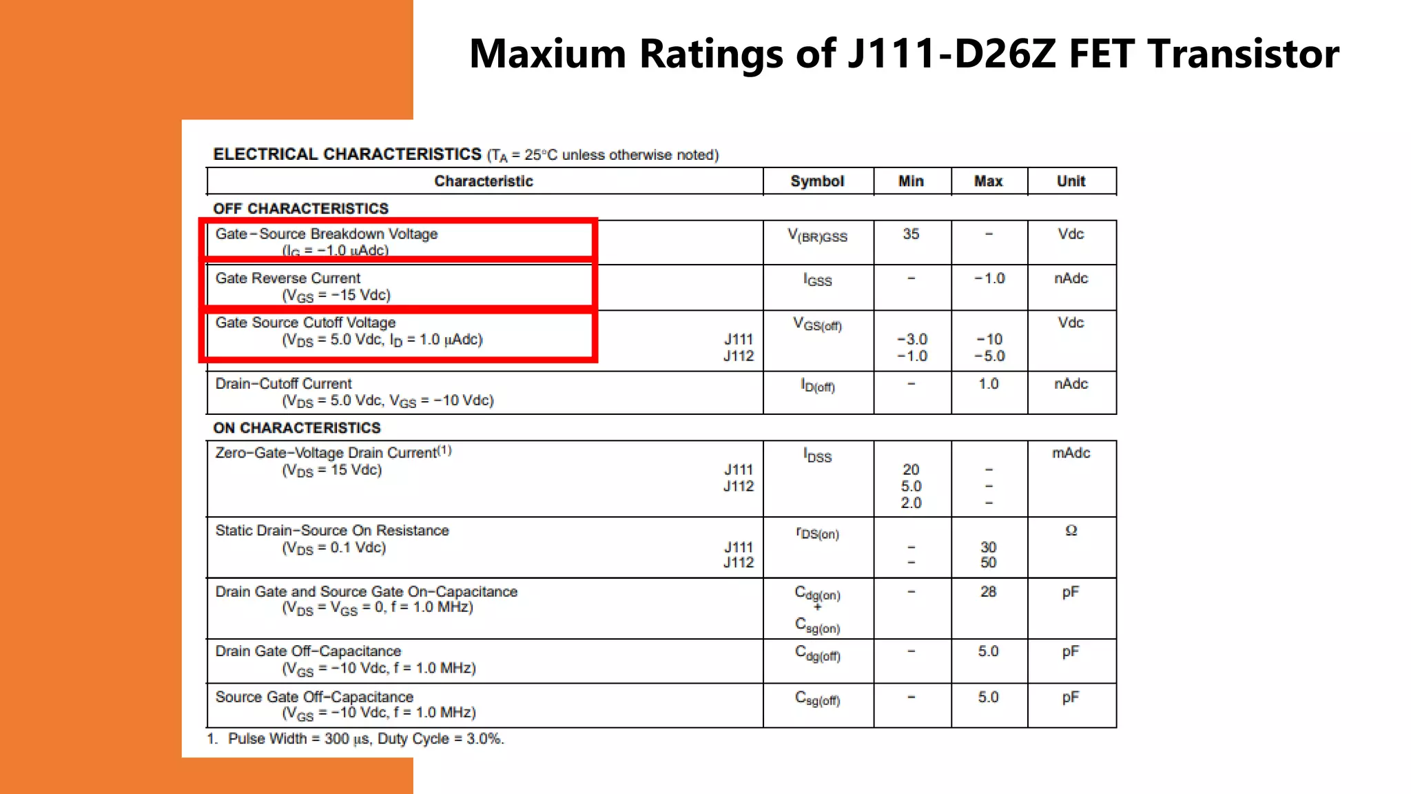
5. Maximum ratings for the J111