Downloaded 641 times

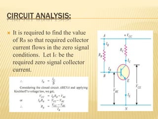
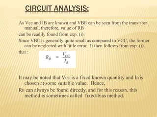
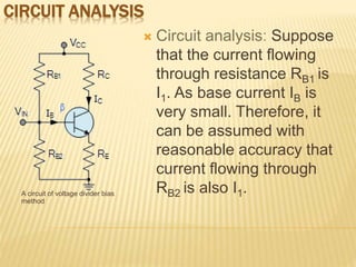
![CIRCUIT ANALYSIS
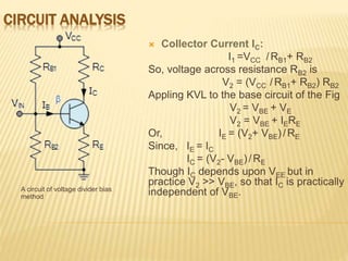
A circuit of voltage divider bias
method
Collector-emitter voltage VCE:
Applying KVL to the collector side.
VCC = ICRC + VCE + IERE
= ICRC + VCE + ICRE
[Because IE = IC]
= IC (RC + RE) + VCE
VCE = VCC – IC (RC + RE)
Stabilisation: In this circuit, excellent
stabilization is provided by RE. We know
that,
V2 = VCC – IC (RC + RE)
Suppose the collector current IC
increases due to rise in temperature.
This will cause the voltage drop across
emitter resistance RE to increases. As
voltage drop across R2 is independent
of IC therefore, VBE decreases. This in
turn causes IB to decrease. The
reduced value of IB tends to restore IC
to the original value.](https://image.slidesharecdn.com/transistorbiasing-161128173414/85/Transistor-biasing-14-320.jpg)


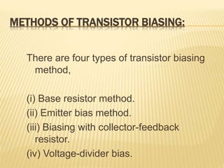
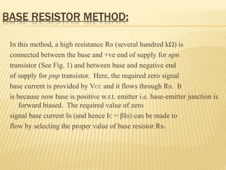
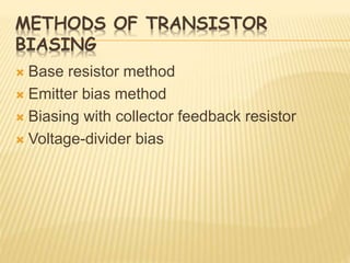
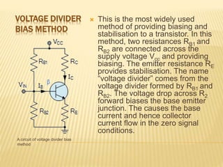
There are four main methods of transistor biasing: base resistor method, emitter bias method, biasing with collector feedback resistor, and voltage-divider bias method. The document then focuses on explaining the base resistor method and voltage-divider bias method in more detail. For the base resistor method, a resistor is used to provide base current, but it has poor stability. For the voltage-divider bias method, two resistors are used to provide stable biasing of the transistor by controlling the base-emitter voltage. This method is widely used due to its stability from the emitter resistor preventing changes in collector current.