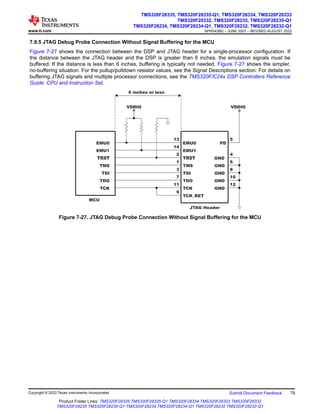
Download to read offline
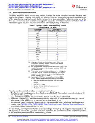
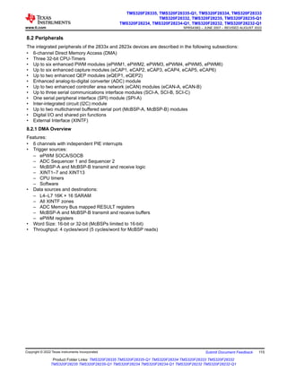
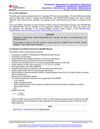
![TMS320F2833x, TMS320F2823x Real-Time Microcontrollers
1 Features
• High-performance static CMOS technology
– Up to 150 MHz (6.67-ns cycle time)
– 1.9-V/1.8-V core, 3.3-V I/O design
• High-performance 32-bit CPU (TMS320C28x)
– IEEE 754 single-precision Floating-Point Unit
(FPU) (F2833x only)
– 16 × 16 and 32 × 32 MAC operations
– 16 × 16 dual MAC
– Harvard bus architecture
– Fast interrupt response and processing
– Unified memory programming model
– Code-efficient (in C/C++ and Assembly)
• Six-channel DMA controller (for ADC, McBSP,
ePWM, XINTF, and SARAM)
• 16-bit or 32-bit External Interface (XINTF)
– More than 2M × 16 address reach
• On-chip memory
– F28335, F28333, F28235:
256K × 16 flash, 34K × 16 SARAM
– F28334, F28234:
128K × 16 flash, 34K × 16 SARAM
– F28332, F28232:
64K × 16 flash, 26K × 16 SARAM
– 1K × 16 OTP ROM
• Boot ROM (8K × 16)
– With software boot modes (through SCI, SPI,
CAN, I2C, McBSP, XINTF, and parallel I/O)
– Standard math tables
• Clock and system control
– On-chip oscillator
– Watchdog timer module
• GPIO0 to GPIO63 pins can be connected to one of
the eight external core interrupts
• Peripheral Interrupt Expansion (PIE) block that
supports all 58 peripheral interrupts
• 128-bit security key/lock
– Protects flash/OTP/RAM blocks
– Prevents firmware reverse-engineering
• Enhanced control peripherals
– Up to 18 PWM outputs
– Up to 6 HRPWM outputs with 150-ps MEP
resolution
– Up to 6 event capture inputs
– Up to 2 Quadrature Encoder interfaces
– Up to 8 32-bit timers
(6 for eCAPs and 2 for eQEPs)
– Up to 9 16-bit timers
(6 for ePWMs and 3 XINTCTRs)
• Three 32-bit CPU timers
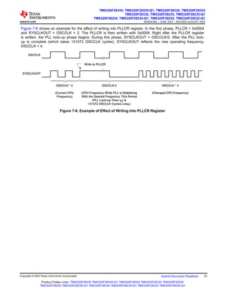
• Serial port peripherals
– Up to 2 CAN modules
– Up to 3 SCI (UART) modules
– Up to 2 McBSP modules (configurable as SPI)
– One SPI module
– One Inter-Integrated Circuit (I2C) bus
• 12-bit ADC, 16 channels
– 80-ns conversion rate
– 2 × 8 channel input multiplexer
– Two sample-and-hold
– Single/simultaneous conversions
– Internal or external reference
• Up to 88 individually programmable, multiplexed
GPIO pins with input filtering
• JTAG boundary scan support
– IEEE Standard 1149.1-1990 Standard Test
Access Port and Boundary Scan Architecture
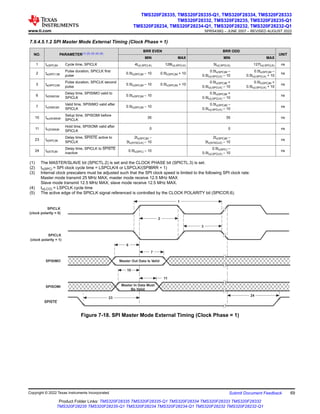
• Advanced debug features
– Analysis and breakpoint functions
– Real-time debug using hardware
• Development support includes
– ANSI C/C++ compiler/assembler/linker
– Code Composer Studio™ IDE
– DSP/BIOS™ and SYS/BIOS
– Digital motor control and digital power software
libraries
• Low-power modes and power savings
– IDLE, STANDBY, HALT modes supported
– Disable individual peripheral clocks
• Endianness: Little endian
• Package options:
– Lead-free, green packaging
– 176-ball plastic Ball Grid Array (BGA) [ZJZ]
– 179-ball MicroStar BGA™ [ZHH]
– 179-ball New Fine Pitch Ball Grid Array
(nFBGA) [ZAY]
– 176-pin Low-Profile Quad Flatpack (LQFP)
[PGF]
– 176-pin Thermally Enhanced Low-Profile Quad
Flatpack (HLQFP) [PTP]
• Temperature options:
– A: –40°C to 85°C (PGF, ZHH, ZAY, ZJZ)
– S: –40°C to 125°C (PTP, ZJZ)
– Q: –40°C to 125°C (PTP, ZJZ)
(AEC Q100 qualification for automotive
applications)
TMS320F28335, TMS320F28335-Q1, TMS320F28334, TMS320F28333
TMS320F28332, TMS320F28235, TMS320F28235-Q1
TMS320F28234, TMS320F28234-Q1, TMS320F28232, TMS320F28232-Q1
SPRS439Q – JUNE 2007 – REVISED AUGUST 2022
An IMPORTANT NOTICE at the end of this data sheet addresses availability, warranty, changes, use in safety-critical applications,
intellectual property matters and other important disclaimers. PRODUCTION DATA.](https://image.slidesharecdn.com/tms320f28335-231214074210-26d2911a/85/tms320f28335-pdf-1-320.jpg)
![TMS320F2833x, TMS320F2823x Real-Time Microcontrollers
1 Features
• High-performance static CMOS technology
– Up to 150 MHz (6.67-ns cycle time)
– 1.9-V/1.8-V core, 3.3-V I/O design
• High-performance 32-bit CPU (TMS320C28x)
– IEEE 754 single-precision Floating-Point Unit
(FPU) (F2833x only)
– 16 × 16 and 32 × 32 MAC operations
– 16 × 16 dual MAC
– Harvard bus architecture
– Fast interrupt response and processing
– Unified memory programming model
– Code-efficient (in C/C++ and Assembly)
• Six-channel DMA controller (for ADC, McBSP,
ePWM, XINTF, and SARAM)
• 16-bit or 32-bit External Interface (XINTF)
– More than 2M × 16 address reach
• On-chip memory
– F28335, F28333, F28235:
256K × 16 flash, 34K × 16 SARAM
– F28334, F28234:
128K × 16 flash, 34K × 16 SARAM
– F28332, F28232:
64K × 16 flash, 26K × 16 SARAM
– 1K × 16 OTP ROM
• Boot ROM (8K × 16)
– With software boot modes (through SCI, SPI,
CAN, I2C, McBSP, XINTF, and parallel I/O)
– Standard math tables
• Clock and system control
– On-chip oscillator
– Watchdog timer module
• GPIO0 to GPIO63 pins can be connected to one of
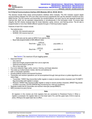
the eight external core interrupts
• Peripheral Interrupt Expansion (PIE) block that
supports all 58 peripheral interrupts
• 128-bit security key/lock
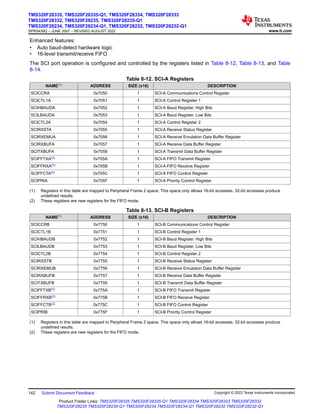
– Protects flash/OTP/RAM blocks
– Prevents firmware reverse-engineering
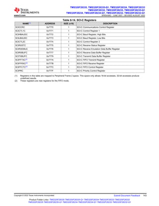
• Enhanced control peripherals
– Up to 18 PWM outputs
– Up to 6 HRPWM outputs with 150-ps MEP
resolution
– Up to 6 event capture inputs
– Up to 2 Quadrature Encoder interfaces
– Up to 8 32-bit timers
(6 for eCAPs and 2 for eQEPs)
– Up to 9 16-bit timers
(6 for ePWMs and 3 XINTCTRs)
• Three 32-bit CPU timers
• Serial port peripherals
– Up to 2 CAN modules
– Up to 3 SCI (UART) modules
– Up to 2 McBSP modules (configurable as SPI)
– One SPI module
– One Inter-Integrated Circuit (I2C) bus
• 12-bit ADC, 16 channels
– 80-ns conversion rate
– 2 × 8 channel input multiplexer
– Two sample-and-hold
– Single/simultaneous conversions
– Internal or external reference
• Up to 88 individually programmable, multiplexed
GPIO pins with input filtering
• JTAG boundary scan support
– IEEE Standard 1149.1-1990 Standard Test
Access Port and Boundary Scan Architecture
• Advanced debug features
– Analysis and breakpoint functions
– Real-time debug using hardware
• Development support includes
– ANSI C/C++ compiler/assembler/linker
– Code Composer Studio™ IDE
– DSP/BIOS™ and SYS/BIOS
– Digital motor control and digital power software
libraries
• Low-power modes and power savings
– IDLE, STANDBY, HALT modes supported
– Disable individual peripheral clocks
• Endianness: Little endian
• Package options:
– Lead-free, green packaging
– 176-ball plastic Ball Grid Array (BGA) [ZJZ]
– 179-ball MicroStar BGA™ [ZHH]
– 179-ball New Fine Pitch Ball Grid Array
(nFBGA) [ZAY]
– 176-pin Low-Profile Quad Flatpack (LQFP)
[PGF]
– 176-pin Thermally Enhanced Low-Profile Quad
Flatpack (HLQFP) [PTP]
• Temperature options:
– A: –40°C to 85°C (PGF, ZHH, ZAY, ZJZ)
– S: –40°C to 125°C (PTP, ZJZ)
– Q: –40°C to 125°C (PTP, ZJZ)
(AEC Q100 qualification for automotive
applications)
TMS320F28335, TMS320F28335-Q1, TMS320F28334, TMS320F28333
TMS320F28332, TMS320F28235, TMS320F28235-Q1
TMS320F28234, TMS320F28234-Q1, TMS320F28232, TMS320F28232-Q1
SPRS439Q – JUNE 2007 – REVISED AUGUST 2022
An IMPORTANT NOTICE at the end of this data sheet addresses availability, warranty, changes, use in safety-critical applications,
intellectual property matters and other important disclaimers. PRODUCTION DATA.](https://image.slidesharecdn.com/tms320f28335-231214074210-26d2911a/75/tms320f28335-pdf-1-2048.jpg)
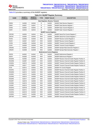
![4 Revision History
Changes from February 2, 2021 to August 8, 2022 (from Revision P (February 2021) to
Revision Q (August 2022)) Page
• Global: Changed document title from TMS320F2833x, TMS320F2823x Digital Signal Controllers (DSCs) to
TMS320F2833x, TMS320F2823x Real-Time Microcontrollers. .........................................................................1
• Global: Changed "digital signal controller" to "real-time microcontroller". Changed "DSC" to "MCU". .............1
• Global: Due to an equipment End-of_Life notice from our substrate supplier, we are phasing out certain
MicroStar BGA™ packaging devices. These devices have now been converted to a New Fine Pitch Ball Grid
Array (nFBGA) package. For more information, see the Package Redesign Details section.............................1
• Global: Added 179-ball ZAY New Fine Pitch Ball Grid Array (nFBGA)..............................................................1
• Global: Changed title of errata from TMS320F2833x, TMS320F2823x DSCs Silicon Errata to
TMS320F2833x, TMS320F2823x Real-Time MCUs Silicon Errata....................................................................1
• Global: Replaced references to peripheral reference guides with references to the TMS320x2833x,
TMS320x2823x Real-Time Microcontrollers Technical Reference Manual........................................................ 1
• Global: Replaced "emulator" with "JTAG debug probe".....................................................................................1
• Section 1 (Features): Changed "Advanced emulation features" to "Advanced debug features"........................1
• Section 1: Added "179-ball New Fine Pitch Ball Grid Array (nFBGA) [ZAY]" to "Package options"................... 1
• Section 1: Added "ZAY" to Temperature option "A"............................................................................................ 1
• Section 2 (Applications): Updated section..........................................................................................................2
• Section 3 (Description): Updated section. Changed Device Information table to Package Information table.
Added ZAY nFBGA to Package Information table.............................................................................................. 2
• Table 5-1 (F2833x Device Comparison): Appended "(UART-compatible)" to "Serial Communications Interface
(SCI)".................................................................................................................................................................. 8
• Table 5-1: Added "179-Ball ZAY" to Packaging section. Added ZAY to "A" Temperature option........................8
• Table 5-2 (F2823x Device Comparison): Appended "(UART-compatible)" to "Serial Communications Interface
(SCI)".................................................................................................................................................................. 8
• Table 5-2: Added "179-Ball ZAY" to Packaging section. Added ZAY to "A" Temperature option........................8
• Section 5.1 (Related Products): Updated section. ........................................................................................... 11
• Section 6.1 (Pin Diagrams): Added 179-ball ZAY new fine pitch ball grid array (nFBGA)................................12
• Table 6-1 (Signal Descriptions): Added ZAY package...................................................................................... 22
• Table 6-1: Updated DESCRIPTION of EMU0, EMU1, and XRS...................................................................... 22
• Section 7.3 (ESD Ratings – Commercial): Add data for ZAY package.............................................................33
• Section 7.5.3 (Reducing Current Consumption): Updated list of methods to reduce power consumption.......38
• Section 7.7.4 (ZAY Package): Added table.......................................................................................................44
• Section 7.9.2 (Power Sequencing): Updated "No requirements are placed on the power-up and power-down
sequences ..." paragraph..................................................................................................................................48
• Section 7.9.5: Changed section title from "Emulator Connection Without Signal Buffering for the DSP" to
"JTAG Debug Probe Connection Without Signal Buffering for the MCU".........................................................79
• Figure 7-27: Changed figure title from "Emulator Connection Without Signal Buffering for the DSP" to "JTAG
Debug Probe Connection Without Signal Buffering for the MCU".................................................................... 79
• Figure 7-27 (Emulator Connection Without Signal Buffering for the MCU): Changed "DSC" to "MCU"...........79
• Section 7.9.6.8.2 (Synchronous XREADY Timing Requirements (Ready-on-Write, One Wait State)): Restored
footnote.............................................................................................................................................................92
• Table 8-14 (SCI-C Registers): Restored footnotes......................................................................................... 141
• Figure 8-15 (Serial Communications Interface (SCI) Module Block Diagram): Updated figure......................141
• Figure 8-34 (Watchdog Module): Updated figure............................................................................................179
• Section 9.1: Changed title from "TI Design or Reference Design" to "TI Reference Design".........................181
• Section 9.1 (TI Reference Design): Updated section..................................................................................... 181
• Section 10 (Device and Documentation Support): Updated section...............................................................182
• Section 10.1: Changed title from "Getting Started" to "Getting Started and Next Steps". Updated section... 182
• Figure 10-1 (Example of F2833x, F2823x Device Nomenclature): Added 179-ball ZAY package under
PACKAGE TYPE............................................................................................................................................ 182
TMS320F28335, TMS320F28335-Q1, TMS320F28334, TMS320F28333
TMS320F28332, TMS320F28235, TMS320F28235-Q1
TMS320F28234, TMS320F28234-Q1, TMS320F28232, TMS320F28232-Q1
SPRS439Q – JUNE 2007 – REVISED AUGUST 2022 www.ti.com
6 Submit Document Feedback Copyright © 2022 Texas Instruments Incorporated
Product Folder Links: TMS320F28335 TMS320F28335-Q1 TMS320F28334 TMS320F28333 TMS320F28332
TMS320F28235 TMS320F28235-Q1 TMS320F28234 TMS320F28234-Q1 TMS320F28232 TMS320F28232-Q1](https://image.slidesharecdn.com/tms320f28335-231214074210-26d2911a/85/tms320f28335-pdf-6-320.jpg)
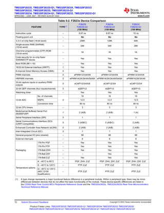

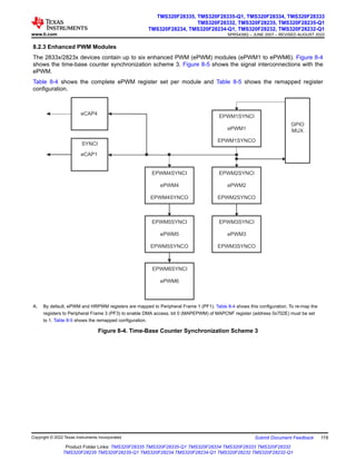
![Table 6-1. Signal Descriptions (continued)
NAME
PIN NO.
DESCRIPTION (1)
PGF,
PTP
PIN #
ZHH,
ZAY
BALL #
ZJZ
BALL #
CLOCK
XCLKOUT 138 C11 A10
Output clock derived from SYSCLKOUT. XCLKOUT is either the same frequency, one-half
the frequency, or one-fourth the frequency of SYSCLKOUT. This is controlled by bits
18:16 (XTIMCLK) and bit 2 (CLKMODE) in the XINTCNF2 register. At reset, XCLKOUT =
SYSCLKOUT/4. The XCLKOUT signal can be turned off by setting XINTCNF2[CLKOFF]
to 1. Unlike other GPIO pins, the XCLKOUT pin is not placed in high-impedance state
during a reset. (O/Z, 8 mA drive).
XCLKIN 105 J14 G13
External Oscillator Input. This pin is to feed a clock from an external 3.3-V oscillator. In this
case, the X1 pin must be tied to GND. If a crystal/resonator is used (or if an external 1.9-V
oscillator is used to feed clock to X1 pin), this pin must be tied to GND. (I)
X1 104 J13 G14
Internal/External Oscillator Input. To use the internal oscillator, a quartz crystal or a
ceramic resonator may be connected across X1 and X2. The X1 pin is referenced to the
1.9-V/1.8-V core digital power supply. A 1.9-V/1.8-V external oscillator may be connected
to the X1 pin. In this case, the XCLKIN pin must be connected to ground. If a 3.3-V
external oscillator is used with the XCLKIN pin, X1 must be tied to GND. (I)
X2 102 J11 H14
Internal Oscillator Output. A quartz crystal or a ceramic resonator may be connected
across X1 and X2. If X2 is not used, it must be left unconnected. (O)
RESET
XRS 80 L10 M13
Device Reset (in) and Watchdog Reset (out).
Device reset. XRS causes the device to terminate execution. The PC will point to the
address contained at the location 0x3FFFC0. When XRS is brought to a high level,
execution begins at the location pointed to by the PC. This pin is driven low by the MCU
when a watchdog reset occurs. During watchdog reset, the XRS pin is driven low for the
watchdog reset duration of 512 OSCCLK cycles. (I/OD, ↑)
The output buffer of this pin is an open drain with an internal pullup. If this pin is driven by
an external device, it should be done using an open-drain device.
An external R-C circuit may be used on the pin, taking care that the timing requirements
during power down are still met.
ADC SIGNALS
ADCINA7 35 K4 K1 ADC Group A, Channel 7 input (I)
ADCINA6 36 J5 K2 ADC Group A, Channel 6 input (I)
ADCINA5 37 L1 L1 ADC Group A, Channel 5 input (I)
ADCINA4 38 L2 L2 ADC Group A, Channel 4 input (I)
ADCINA3 39 L3 L3 ADC Group A, Channel 3 input (I)
ADCINA2 40 M1 M1 ADC Group A, Channel 2 input (I)
ADCINA1 41 N1 M2 ADC Group A, Channel 1 input (I)
ADCINA0 42 M3 M3 ADC Group A, Channel 0 input (I)
ADCINB7 53 K5 N6 ADC Group B, Channel 7 input (I)
ADCINB6 52 P4 M6 ADC Group B, Channel 6 input (I)
ADCINB5 51 N4 N5 ADC Group B, Channel 5 input (I)
ADCINB4 50 M4 M5 ADC Group B, Channel 4 input (I)
ADCINB3 49 L4 N4 ADC Group B, Channel 3 input (I)
ADCINB2 48 P3 M4 ADC Group B, Channel 2 input (I)
ADCINB1 47 N3 N3 ADC Group B, Channel 1 input (I)
ADCINB0 46 P2 P3 ADC Group B, Channel 0 input (I)
ADCLO 43 M2 N2 Low Reference (connect to analog ground) (I)
ADCRESEXT 57 M5 P6 ADC External Current Bias Resistor. Connect a 22-kΩ resistor to analog ground.
ADCREFIN 54 L5 P7 External reference input (I)
www.ti.com
TMS320F28335, TMS320F28335-Q1, TMS320F28334, TMS320F28333
TMS320F28332, TMS320F28235, TMS320F28235-Q1
TMS320F28234, TMS320F28234-Q1, TMS320F28232, TMS320F28232-Q1
SPRS439Q – JUNE 2007 – REVISED AUGUST 2022
Copyright © 2022 Texas Instruments Incorporated Submit Document Feedback 23
Product Folder Links: TMS320F28335 TMS320F28335-Q1 TMS320F28334 TMS320F28333 TMS320F28332
TMS320F28235 TMS320F28235-Q1 TMS320F28234 TMS320F28234-Q1 TMS320F28232 TMS320F28232-Q1](https://image.slidesharecdn.com/tms320f28335-231214074210-26d2911a/85/tms320f28335-pdf-23-320.jpg)
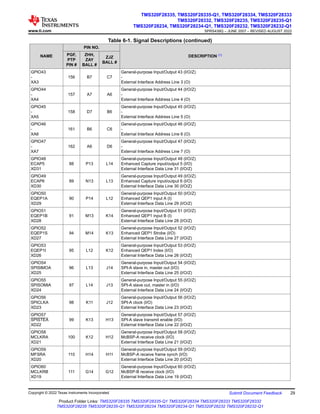
![Table 6-1. Signal Descriptions (continued)
NAME
PIN NO.
DESCRIPTION (1)
PGF,
PTP
PIN #
ZHH,
ZAY
BALL #
ZJZ
BALL #
GPIO5
EPWM3B
MFSRA
ECAP1
12 E3 E3
General-purpose input/output 5 (I/O/Z)
Enhanced PWM3 output B (O)
McBSP-A receive frame synch (I/O)
Enhanced Capture input/output 1 (I/O)
GPIO6
EPWM4A
EPWMSYNCI
EPWMSYNCO
13 E1 F1
General-purpose input/output 6 (I/O/Z)
Enhanced PWM4 output A and HRPWM channel (O)
External ePWM sync pulse input (I)
External ePWM sync pulse output (O)
GPIO7
EPWM4B
MCLKRA
ECAP2
16 F2 F2
General-purpose input/output 7 (I/O/Z)
Enhanced PWM4 output B (O)
McBSP-A receive clock (I/O)
Enhanced capture input/output 2 (I/O)
GPIO8
EPWM5A
CANTXB
ADCSOCAO
17 F1 F3
General-purpose Input/Output 8 (I/O/Z)
Enhanced PWM5 output A and HRPWM channel (O)
Enhanced CAN-B transmit (O)
ADC start-of-conversion A (O)
GPIO9
EPWM5B
SCITXDB
ECAP3
18 G5 G1
General-purpose input/output 9 (I/O/Z)
Enhanced PWM5 output B (O)
SCI-B transmit data(O)
Enhanced capture input/output 3 (I/O)
GPIO10
EPWM6A
CANRXB
ADCSOCBO
19 G4 G2
General-purpose input/output 10 (I/O/Z)
Enhanced PWM6 output A and HRPWM channel (O)
Enhanced CAN-B receive (I)
ADC start-of-conversion B (O)
GPIO11
EPWM6B
SCIRXDB
ECAP4
20 G2 G3
General-purpose input/output 11 (I/O/Z)
Enhanced PWM6 output B (O)
SCI-B receive data (I)
Enhanced CAP Input/Output 4 (I/O)
GPIO12
TZ1
CANTXB
MDXB
21 G3 H1
General-purpose input/output 12 (I/O/Z)
Trip Zone input 1 (I)
Enhanced CAN-B transmit (O)
McBSP-B transmit serial data (O)
GPIO13
TZ2
CANRXB
MDRB
24 H3 H2
General-purpose input/output 13 (I/O/Z)
Trip Zone input 2 (I)
Enhanced CAN-B receive (I)
McBSP-B receive serial data (I)
GPIO14
25 H2 H3
General-purpose input/output 14 (I/O/Z)
TZ3/ XHOLD
Trip Zone input 3/External Hold Request. XHOLD, when active (low), requests the external
interface (XINTF) to release the external bus and place all buses and strobes into a high-
impedance state. To prevent this from happening when TZ3 signal goes active, disable this
function by writing XINTCNF2[HOLD] = 1. If this is not done, the XINTF bus will go into
high impedance anytime TZ3 goes low. On the ePWM side, TZn signals are ignored by
default, unless they are enabled by the code. The XINTF will release the bus when any
current access is complete and there are no pending accesses on the XINTF. (I)
SCITXDB SCI-B Transmit (O)
MCLKXB McBSP-B transmit clock (I/O)
TMS320F28335, TMS320F28335-Q1, TMS320F28334, TMS320F28333
TMS320F28332, TMS320F28235, TMS320F28235-Q1
TMS320F28234, TMS320F28234-Q1, TMS320F28232, TMS320F28232-Q1
SPRS439Q – JUNE 2007 – REVISED AUGUST 2022 www.ti.com
26 Submit Document Feedback Copyright © 2022 Texas Instruments Incorporated
Product Folder Links: TMS320F28335 TMS320F28335-Q1 TMS320F28334 TMS320F28333 TMS320F28332
TMS320F28235 TMS320F28235-Q1 TMS320F28234 TMS320F28234-Q1 TMS320F28232 TMS320F28232-Q1](https://image.slidesharecdn.com/tms320f28335-231214074210-26d2911a/85/tms320f28335-pdf-26-320.jpg)
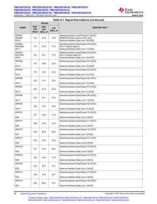
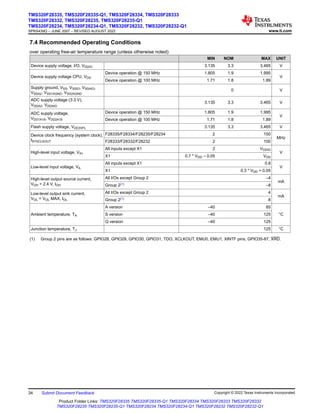
![7.7 Thermal Resistance Characteristics
7.7.1 PGF Package
°C/W(1) (2) AIR FLOW (lfm)(3)
RΘJC Junction-to-case 8.2 0
RΘJB Junction-to-board 28.1 0
RΘJA
(High k PCB)
Junction-to-free air
44 0
34.5 150
33 250
31 500
PsiJT Junction-to-package top
0.12 0
0.48 150
0.57 250
0.74 500
PsiJB Junction-to-board
28.1 0
26.3 150
25.9 250
25.2 500
(1) °C/W = degrees Celsius per watt
(2) These values are based on a JEDEC-defined 2S2P system (with the exception of the Theta JC [RΘJC] value, which is based on
a JEDEC-defined 1S0P system) and will change based on environment as well as application. For more information, see these
EIA/JEDEC standards:
• JESD51-2, Integrated Circuits Thermal Test Method Environmental Conditions - Natural Convection (Still Air)
• JESD51-3, Low Effective Thermal Conductivity Test Board for Leaded Surface Mount Packages
• JESD51-7, High Effective Thermal Conductivity Test Board for Leaded Surface Mount Packages
• JESD51-9, Test Boards for Area Array Surface Mount Package Thermal Measurements
(3) lfm = linear feet per minute
www.ti.com
TMS320F28335, TMS320F28335-Q1, TMS320F28334, TMS320F28333
TMS320F28332, TMS320F28235, TMS320F28235-Q1
TMS320F28234, TMS320F28234-Q1, TMS320F28232, TMS320F28232-Q1
SPRS439Q – JUNE 2007 – REVISED AUGUST 2022
Copyright © 2022 Texas Instruments Incorporated Submit Document Feedback 41
Product Folder Links: TMS320F28335 TMS320F28335-Q1 TMS320F28334 TMS320F28333 TMS320F28332
TMS320F28235 TMS320F28235-Q1 TMS320F28234 TMS320F28234-Q1 TMS320F28232 TMS320F28232-Q1](https://image.slidesharecdn.com/tms320f28335-231214074210-26d2911a/85/tms320f28335-pdf-41-320.jpg)
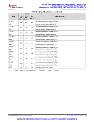
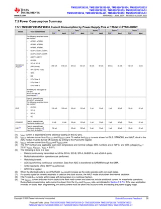
![7.7.2 PTP Package
°C/W(1) (2) AIR FLOW (lfm)(3)
RΘJC Junction-to-case 12.1 0
RΘJB Junction-to-board 5.1 0
RΘJA
(High k PCB)
Junction-to-free air
17.4 0
11.7 150
10.1 250
8.8 500
PsiJT Junction-to-package top
0.2 0
0.3 150
0.4 250
0.5 500
PsiJB Junction-to-board
5.0 0
4.7 150
4.7 250
4.6 500
(1) °C/W = degrees Celsius per watt
(2) These values are based on a JEDEC-defined 2S2P system (with the exception of the Theta JC [RΘJC] value, which is based on
a JEDEC-defined 1S0P system) and will change based on environment as well as application. For more information, see these
EIA/JEDEC standards:
• JESD51-2, Integrated Circuits Thermal Test Method Environmental Conditions - Natural Convection (Still Air)
• JESD51-3, Low Effective Thermal Conductivity Test Board for Leaded Surface Mount Packages
• JESD51-7, High Effective Thermal Conductivity Test Board for Leaded Surface Mount Packages
• JESD51-9, Test Boards for Area Array Surface Mount Package Thermal Measurements
(3) lfm = linear feet per minute
TMS320F28335, TMS320F28335-Q1, TMS320F28334, TMS320F28333
TMS320F28332, TMS320F28235, TMS320F28235-Q1
TMS320F28234, TMS320F28234-Q1, TMS320F28232, TMS320F28232-Q1
SPRS439Q – JUNE 2007 – REVISED AUGUST 2022 www.ti.com
42 Submit Document Feedback Copyright © 2022 Texas Instruments Incorporated
Product Folder Links: TMS320F28335 TMS320F28335-Q1 TMS320F28334 TMS320F28333 TMS320F28332
TMS320F28235 TMS320F28235-Q1 TMS320F28234 TMS320F28234-Q1 TMS320F28232 TMS320F28232-Q1](https://image.slidesharecdn.com/tms320f28335-231214074210-26d2911a/85/tms320f28335-pdf-42-320.jpg)
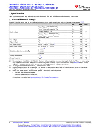
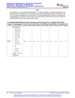
![7.7.3 ZHH Package
°C/W(1) (2) AIR FLOW (lfm)(3)
RΘJC Junction-to-case 8.8 0
RΘJB Junction-to-board 12.5 0
RΘJA
(High k PCB)
Junction-to-free air
32.8 0
24.1 150
22.9 250
20.9 500
PsiJT Junction-to-package top
0.09 0
0.3 150
0.36 250
0.48 500
PsiJB Junction-to-board
12.4 0
11.8 150
11.7 250
11.5 500
(1) °C/W = degrees Celsius per watt
(2) These values are based on a JEDEC-defined 2S2P system (with the exception of the Theta JC [RΘJC] value, which is based on
a JEDEC-defined 1S0P system) and will change based on environment as well as application. For more information, see these
EIA/JEDEC standards:
• JESD51-2, Integrated Circuits Thermal Test Method Environmental Conditions - Natural Convection (Still Air)
• JESD51-3, Low Effective Thermal Conductivity Test Board for Leaded Surface Mount Packages
• JESD51-7, High Effective Thermal Conductivity Test Board for Leaded Surface Mount Packages
• JESD51-9, Test Boards for Area Array Surface Mount Package Thermal Measurements
(3) lfm = linear feet per minute
www.ti.com
TMS320F28335, TMS320F28335-Q1, TMS320F28334, TMS320F28333
TMS320F28332, TMS320F28235, TMS320F28235-Q1
TMS320F28234, TMS320F28234-Q1, TMS320F28232, TMS320F28232-Q1
SPRS439Q – JUNE 2007 – REVISED AUGUST 2022
Copyright © 2022 Texas Instruments Incorporated Submit Document Feedback 43
Product Folder Links: TMS320F28335 TMS320F28335-Q1 TMS320F28334 TMS320F28333 TMS320F28332
TMS320F28235 TMS320F28235-Q1 TMS320F28234 TMS320F28234-Q1 TMS320F28232 TMS320F28232-Q1](https://image.slidesharecdn.com/tms320f28335-231214074210-26d2911a/85/tms320f28335-pdf-43-320.jpg)
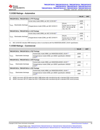
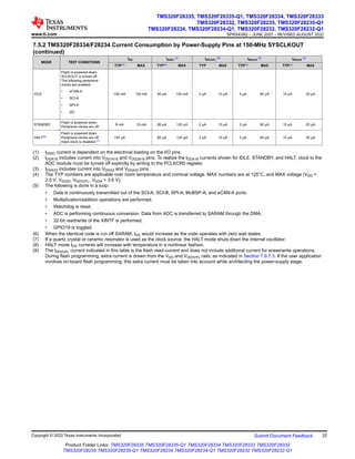
![7.7.4 ZAY Package
°C/W(1) (2) AIR FLOW (m/s)(3)
RΘJC Junction-to-case 9.4 0
RΘJB Junction-to-board 13.5 0
RΘJA
(High k PCB)
Junction-to-free air
28.5 0
22.8 1
21.6 2
20.8 3
PsiJT Junction-to-package top
0.27 0
0.5 1
0.7 2
0.8 3
PsiJB Junction-to-board
13.3 0
13.2 1
13 2
12.9 3
(1) °C/W = degrees Celsius per watt
(2) These values are based on a JEDEC-defined 2S2P system (with the exception of the Theta JC [RΘJC] value, which is based on
a JEDEC-defined 1S0P system) and will change based on environment as well as application. For more information, see these
EIA/JEDEC standards:
• JESD51-2, Integrated Circuits Thermal Test Method Environmental Conditions - Natural Convection (Still Air)
• JESD51-3, Low Effective Thermal Conductivity Test Board for Leaded Surface Mount Packages
• JESD51-7, High Effective Thermal Conductivity Test Board for Leaded Surface Mount Packages
• JESD51-9, Test Boards for Area Array Surface Mount Package Thermal Measurements
(3) m/s = meter per second
TMS320F28335, TMS320F28335-Q1, TMS320F28334, TMS320F28333
TMS320F28332, TMS320F28235, TMS320F28235-Q1
TMS320F28234, TMS320F28234-Q1, TMS320F28232, TMS320F28232-Q1
SPRS439Q – JUNE 2007 – REVISED AUGUST 2022 www.ti.com
44 Submit Document Feedback Copyright © 2022 Texas Instruments Incorporated
Product Folder Links: TMS320F28335 TMS320F28335-Q1 TMS320F28334 TMS320F28333 TMS320F28332
TMS320F28235 TMS320F28235-Q1 TMS320F28234 TMS320F28234-Q1 TMS320F28232 TMS320F28232-Q1](https://image.slidesharecdn.com/tms320f28335-231214074210-26d2911a/85/tms320f28335-pdf-44-320.jpg)
![7.7.5 ZJZ Package
°C/W(1) (2) AIR FLOW (lfm)(3)
RΘJC Junction-to-case 11.4 0
RΘJB Junction-to-board 12 0
RΘJA
(High k PCB)
Junction-to-free air
29.6 0
20.9 150
19.7 250
18 500
PsiJT Junction-to-package top
0.2 0
0.78 150
0.91 250
1.11 500
PsiJB Junction-to-board
12.2 0
11.6 150
11.5 250
11.3 500
(1) °C/W = degrees Celsius per watt
(2) These values are based on a JEDEC-defined 2S2P system (with the exception of the Theta JC [RΘJC] value, which is based on
a JEDEC-defined 1S0P system) and will change based on environment as well as application. For more information, see these
EIA/JEDEC standards:
• JESD51-2, Integrated Circuits Thermal Test Method Environmental Conditions - Natural Convection (Still Air)
• JESD51-3, Low Effective Thermal Conductivity Test Board for Leaded Surface Mount Packages
• JESD51-7, High Effective Thermal Conductivity Test Board for Leaded Surface Mount Packages
• JESD51-9, Test Boards for Area Array Surface Mount Package Thermal Measurements
(3) lfm = linear feet per minute
7.8 Thermal Design Considerations
Based on the end application design and operational profile, the IDD and IDDIO currents could vary. Systems
with more than 1 Watt power dissipation may require a product level thermal design. Care should be taken
to keep Tj within specified limits. In the end applications, Tcase should be measured to estimate the operating
junction temperature Tj. Tcase is normally measured at the center of the package top side surface. The thermal
application note Semiconductor and IC Package Thermal Metrics helps to understand the thermal metrics and
definitions.
www.ti.com
TMS320F28335, TMS320F28335-Q1, TMS320F28334, TMS320F28333
TMS320F28332, TMS320F28235, TMS320F28235-Q1
TMS320F28234, TMS320F28234-Q1, TMS320F28232, TMS320F28232-Q1
SPRS439Q – JUNE 2007 – REVISED AUGUST 2022
Copyright © 2022 Texas Instruments Incorporated Submit Document Feedback 45
Product Folder Links: TMS320F28335 TMS320F28335-Q1 TMS320F28334 TMS320F28333 TMS320F28332
TMS320F28235 TMS320F28235-Q1 TMS320F28234 TMS320F28234-Q1 TMS320F28232 TMS320F28232-Q1](https://image.slidesharecdn.com/tms320f28335-231214074210-26d2911a/85/tms320f28335-pdf-45-320.jpg)
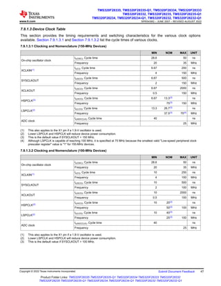

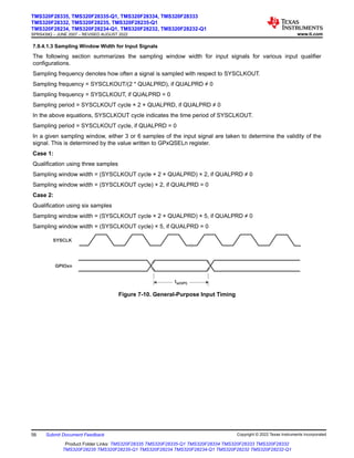
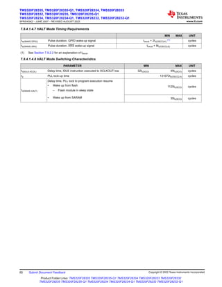
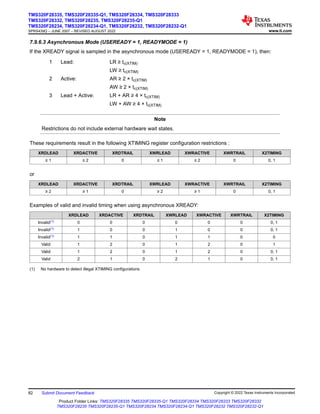
(D)
tw(SP)
tw(IQSW)
A. This glitch will be ignored by the input qualifier. The QUALPRD bit field specifies the qualification sampling period. It can vary from 00 to
0xFF. If QUALPRD = 00, then the sampling period is 1 SYSCLKOUT cycle. For any other value "n", the qualification sampling period in
2n SYSCLKOUT cycles (that is, at every 2n SYSCLKOUT cycles, the GPIO pin will be sampled).
B. The qualification period selected through the GPxCTRL register applies to groups of 8 GPIO pins.
C. The qualification block can take either three or six samples. The GPxQSELn Register selects which sample mode is used.
D. In the example shown, for the qualifier to detect the change, the input should be stable for 10 SYSCLKOUT cycles or greater. In other
words, the inputs should be stable for (5 × QUALPRD × 2) SYSCLKOUT cycles. This would ensure 5 sampling periods for detection to
occur. Because external signals are driven asynchronously, an 13-SYSCLKOUT-wide pulse ensures reliable recognition.
Figure 7-9. Sampling Mode
www.ti.com
TMS320F28335, TMS320F28335-Q1, TMS320F28334, TMS320F28333
TMS320F28332, TMS320F28235, TMS320F28235-Q1
TMS320F28234, TMS320F28234-Q1, TMS320F28232, TMS320F28232-Q1
SPRS439Q – JUNE 2007 – REVISED AUGUST 2022
Copyright © 2022 Texas Instruments Incorporated Submit Document Feedback 55
Product Folder Links: TMS320F28335 TMS320F28335-Q1 TMS320F28334 TMS320F28333 TMS320F28332
TMS320F28235 TMS320F28235-Q1 TMS320F28234 TMS320F28234-Q1 TMS320F28232 TMS320F28232-Q1](https://image.slidesharecdn.com/tms320f28335-231214074210-26d2911a/85/tms320f28335-pdf-55-320.jpg)
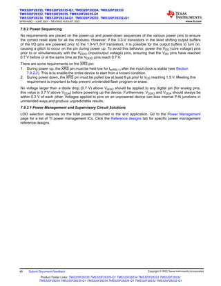
![7.9.4.2.5 Enhanced Quadrature Encoder Pulse (eQEP) Timing
Section 7.9.4.2.5.1 shows the eQEP timing requirement and Section 7.9.4.2.5.2 shows the eQEP switching
characteristics.
7.9.4.2.5.1 Enhanced Quadrature Encoder Pulse (eQEP) Timing Requirements
MIN MAX UNIT
tw(QEPP) QEP input period
Asynchronous(1)/synchronous 2tc(SCO)
cycles
With input qualifier(2) 2[1tc(SCO) + tw(IQSW)]
tw(INDEXH) QEP Index Input High time
Asynchronous(1)/synchronous 2tc(SCO)
cycles
With input qualifier(2) 2tc(SCO) + tw(IQSW)
tw(INDEXL) QEP Index Input Low time
Asynchronous(1)/synchronous 2tc(SCO)
cycles
With input qualifier(2) 2tc(SCO) + tw(IQSW)
tw(STROBH) QEP Strobe High time
Asynchronous(1)/synchronous 2tc(SCO)
cycles
With input qualifier(2) 2tc(SCO) + tw(IQSW)
tw(STROBL) QEP Strobe Input Low time
Asynchronous(1)/synchronous 2tc(SCO)
cycles
With input qualifier(2) 2tc(SCO) + tw(IQSW)
(1) Refer to the TMS320F2833x, TMS320F2823x Real-Time MCUs Silicon Errata for limitations in the asynchronous mode.
(2) For an explanation of the input qualifier parameters, see Section 7.9.4.1.2.1.
7.9.4.2.5.2 eQEP Switching Characteristics
PARAMETER TEST CONDITIONS MIN MAX UNIT
td(CNTR)xin Delay time, external clock to counter increment 4tc(SCO) cycles
td(PCS-OUT)QEP
Delay time, QEP input edge to position compare sync
output
6tc(SCO) cycles
TMS320F28335, TMS320F28335-Q1, TMS320F28334, TMS320F28333
TMS320F28332, TMS320F28235, TMS320F28235-Q1
TMS320F28234, TMS320F28234-Q1, TMS320F28232, TMS320F28232-Q1
SPRS439Q – JUNE 2007 – REVISED AUGUST 2022 www.ti.com
64 Submit Document Feedback Copyright © 2022 Texas Instruments Incorporated
Product Folder Links: TMS320F28335 TMS320F28335-Q1 TMS320F28334 TMS320F28333 TMS320F28332
TMS320F28235 TMS320F28235-Q1 TMS320F28234 TMS320F28234-Q1 TMS320F28232 TMS320F28232-Q1](https://image.slidesharecdn.com/tms320f28335-231214074210-26d2911a/85/tms320f28335-pdf-64-320.jpg)

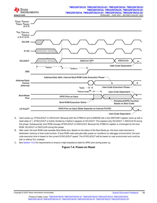
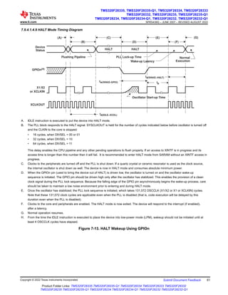
![Unless otherwise specified, all XINTF timing is applicable for the clock configurations listed in Table 7-3.
Table 7-3. XINTF Clock Configurations
MODE SYSCLKOUT XTIMCLK XCLKOUT
1 SYSCLKOUT SYSCLKOUT
Example: 150 MHz 150 MHz 150 MHz
2 SYSCLKOUT 1/2 SYSCLKOUT
Example: 150 MHz 150 MHz 75 MHz
3 1/2 SYSCLKOUT 1/2 SYSCLKOUT
Example: 150 MHz 75 MHz 75 MHz
4 1/2 SYSCLKOUT 1/4 SYSCLKOUT
Example: 150 MHz 75 MHz 37.5 MHz
The relationship between SYSCLKOUT and XTIMCLK is shown in Figure 7-28.
1
0
/2
SYSCLKOUT
C28x
CPU
XINTCNF2 (XTIMCLK)
1
0
/2
XTIMCLK
XINTCNF2
(CLKMODE)
XINTCNF2
(CLKOFF)
0
1
0
XCLKOUT
XTIMING0
XTIMING6
XTIMING7
XBANK
LEAD/ACTIVE/TRAIL
PCLKR3[XINTFENCLK]
Figure 7-28. Relationship Between SYSCLKOUT and XTIMCLK
www.ti.com
TMS320F28335, TMS320F28335-Q1, TMS320F28334, TMS320F28333
TMS320F28332, TMS320F28235, TMS320F28235-Q1
TMS320F28234, TMS320F28234-Q1, TMS320F28232, TMS320F28232-Q1
SPRS439Q – JUNE 2007 – REVISED AUGUST 2022
Copyright © 2022 Texas Instruments Incorporated Submit Document Feedback 83
Product Folder Links: TMS320F28335 TMS320F28335-Q1 TMS320F28334 TMS320F28333 TMS320F28332
TMS320F28235 TMS320F28235-Q1 TMS320F28234 TMS320F28234-Q1 TMS320F28232 TMS320F28232-Q1](https://image.slidesharecdn.com/tms320f28335-231214074210-26d2911a/85/tms320f28335-pdf-83-320.jpg)


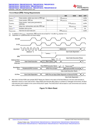
![Lead
Active
Trail
DIN
td(XCOHL-XRDL)
td(XCOH-XA)
td(XCOH-XZCSL)
td(XCOHL-XRDH)
th(XD)XRD
td(XCOHL-XZCSH)
XCLKOUT = XTIMCLK
XCLKOUT = 1/2 XTIMCLK
XZCS0 XZCS6 XZCS7
, ,
XA[0:19]
XRD
XWE0 XWE1
,
(D)
XR/W
XD[0:31], XD[0:15]
tsu(XD)XRD
ta(A)
ta(XRD)
XREADY
(E)
(A)(B) (C)
A. All XINTF accesses (lead period) begin on the rising edge of XCLKOUT. When necessary, the device inserts an alignment cycle before
an access to meet this requirement.
B. During alignment cycles, all signals transition to their inactive state.
C. XA[0:19] holds the last address put on the bus during inactive cycles, including alignment cycles except XA0, which remains high.
D. XWE1 is used in 32-bit data bus mode. In 16-bit mode, this signal is XA0.
E. For USEREADY = 0, the external XREADY input signal is ignored.
Figure 7-29. Example Read Access
XTIMING register parameters used for this example :
XRDLEAD XRDACTIVE XRDTRAIL USEREADY X2TIMING XWRLEAD XWRACTIVE XWRTRAIL READYMODE
≥ 1 ≥ 0 ≥ 0 0 0 N/A(1) N/A(1) N/A(1) N/A(1)
(1) N/A = Not applicable (or "Don’t care") for this example
TMS320F28335, TMS320F28335-Q1, TMS320F28334, TMS320F28333
TMS320F28332, TMS320F28235, TMS320F28235-Q1
TMS320F28234, TMS320F28234-Q1, TMS320F28232, TMS320F28232-Q1
SPRS439Q – JUNE 2007 – REVISED AUGUST 2022 www.ti.com
86 Submit Document Feedback Copyright © 2022 Texas Instruments Incorporated
Product Folder Links: TMS320F28335 TMS320F28335-Q1 TMS320F28334 TMS320F28333 TMS320F28332
TMS320F28235 TMS320F28235-Q1 TMS320F28234 TMS320F28234-Q1 TMS320F28232 TMS320F28232-Q1](https://image.slidesharecdn.com/tms320f28335-231214074210-26d2911a/85/tms320f28335-pdf-86-320.jpg)
![Lead
Active
Trail
td(XCOH-XZCSL)
td(XCOH-XA)
td(XCOHL-XWEL) td(XCOHL-XWEH)
td(XCOHL-XZCSH)
ten(XD)XWEL th(XD)XWEH
tdis(XD)XRNW
XCLKOUT = XTIMCLK
XCLKOUT = 1/2 XTIMCLK
XZCS0 XZCS6 XZCS7
, ,
XRD
XWE0 XWE1
,
(D)
XR/W
XD[0:31], XD[0:15]
td(XCOH-XRNWL) td(XCOHL-XRNWH)
DOUT
XREADY
(E)
td(XWEL-XD)
XA[0:19]
(A) (B) (C)
A. All XINTF accesses (lead period) begin on the rising edge of XCLKOUT. When necessary, the device inserts an alignment cycle before
an access to meet this requirement.
B. During alignment cycles, all signals transition to their inactive state.
C. XA[0:19] holds the last address put on the bus during inactive cycles, including alignment cycles except XA0, which remains high.
D. XWE1 is used in 32-bit data bus mode. In 16-bit mode, this signal is XA0.
E. For USEREADY = 0, the external XREADY input signal is ignored.
Figure 7-30. Example Write Access
XTIMING register parameters used for this example :
XRDLEAD XRDACTIVE XRDTRAIL USEREADY X2TIMING XWRLEAD XWRACTIVE XWRTRAIL READYMODE
N/A(1) N/A(1) N/A(1) 0 0 ≥ 1 ≥ 0 ≥ 0 N/A(1)
(1) N/A = Not applicable (or “Don’t care”) for this example
TMS320F28335, TMS320F28335-Q1, TMS320F28334, TMS320F28333
TMS320F28332, TMS320F28235, TMS320F28235-Q1
TMS320F28234, TMS320F28234-Q1, TMS320F28232, TMS320F28232-Q1
SPRS439Q – JUNE 2007 – REVISED AUGUST 2022 www.ti.com
88 Submit Document Feedback Copyright © 2022 Texas Instruments Incorporated
Product Folder Links: TMS320F28335 TMS320F28335-Q1 TMS320F28334 TMS320F28333 TMS320F28332
TMS320F28235 TMS320F28235-Q1 TMS320F28234 TMS320F28234-Q1 TMS320F28232 TMS320F28232-Q1](https://image.slidesharecdn.com/tms320f28335-231214074210-26d2911a/85/tms320f28335-pdf-88-320.jpg)
![Lead
Active
Trail
DIN
td(XCOH-XZCSL)
td(XCOH-XA)
td(XCOHL-XRDL)
td(XCOHL-XZCSH)
td(XCOHL-XRDH)
WS (Synch)
XCLKOUT = XTIMCLK
XCLKOUT = 1/2 XTIMCLK
XZCS0 XZCS6, XZCS7
XA[0:19]
XRD
XWE0, XWE1 (D)
XR/W
XD[0:31], XD[0:15]
XREADY(Synch)
th(XRDYsynchL)
tsu(XRDYsynchL)XCOHL
tsu(XD)XRD
ta(XRD)
ta(A)
th(XD)XRD
th(XRDYsynchH)XZCSH
= Don’t care. Signal can be high or low during this time.
Legend:
tsu(XRDHsynchH)XCOHL
(F)
te(XRDYsynchH)
(E)
(A) (B) (C)
A. All XINTF accesses (lead period) begin on the rising edge of XCLKOUT. When necessary, the device inserts an alignment cycle before
an access to meet this requirement.
B. During alignment cycles, all signals transition to their inactive state.
C. During inactive cycles, the XINTF address bus always holds the last address put out on the bus except XA0, which remains high. This
includes alignment cycles.
D. XWE1 is valid only in 32-bit data bus mode. In 16-bit mode, this signal is XA0.
E. For each sample, setup time from the beginning of the access (E) can be calculated as: D = (XRDLEAD + XRDACTIVE +n - 1) tc(XTIM) –
tsu(XRDYsynchL)XCOHL
F. Reference for the first sample is with respect to this point: F = (XRDLEAD + XRDACTIVE) tc(XTIM) where n is the sample number: n = 1,
2, 3, and so forth.
Figure 7-31. Example Read With Synchronous XREADY Access
XTIMING register parameters used for this example :
XRDLEAD XRDACTIVE XRDTRAIL USEREADY X2TIMING XWRLEAD XWRACTIVE XWRTRAIL READYMODE
≥ 1 3 ≥ 1 1 0 N/A(1) N/A(1) N/A(1) 0 = XREADY
(Synch)
(1) N/A = “Don’t care” for this example
TMS320F28335, TMS320F28335-Q1, TMS320F28334, TMS320F28333
TMS320F28332, TMS320F28235, TMS320F28235-Q1
TMS320F28234, TMS320F28234-Q1, TMS320F28232, TMS320F28232-Q1
SPRS439Q – JUNE 2007 – REVISED AUGUST 2022 www.ti.com
90 Submit Document Feedback Copyright © 2022 Texas Instruments Incorporated
Product Folder Links: TMS320F28335 TMS320F28335-Q1 TMS320F28334 TMS320F28333 TMS320F28332
TMS320F28235 TMS320F28235-Q1 TMS320F28234 TMS320F28234-Q1 TMS320F28232 TMS320F28232-Q1](https://image.slidesharecdn.com/tms320f28335-231214074210-26d2911a/85/tms320f28335-pdf-90-320.jpg)
![tsu(XD)XRD
Lead
Active
Trail
DIN
td(XCOH-XZCSL)
td(XCOH-XA)
td(XCOHL-XRDL)
td(XCOHL-XZCSH)
td(XCOHL-XRDH)
WS (Async)
XCLKOUT = XTIMCLK
XCLKOUT = 1/2 XTIMCLK
XZCS0, XZCS6, XZCS7
XA[0:19]
XRD
XWE0, XWE1(D)
XR/W
XD[0:31], XD[0:15]
XREADY(Asynch)
tsu(XRDYasynchL)XCOHL
ta(XRD)
ta(A)
th(XRDYasynchL)
th(XD)XRD
th(XRDYasynchH)XZCSH
= Don’t care. Signal can be high or low during this time.
Legend:
(A) (B)
(C)
tsu(XRDYasynchH)XCOHL
(E)
(F)
te(XRDYasynchH)
A. All XINTF accesses (lead period) begin on the rising edge of XCLKOUT. When necessary, the device will insert an alignment cycle
before an access to meet this requirement.
B. During alignment cycles, all signals will transition to their inactive state.
C. During inactive cycles, the XINTF address bus will always hold the last address put out on the bus except XA0, which remains high.
This includes alignment cycles.
D. XWE1 is valid only in 32-bit data bus mode. In 16-bit mode, this signal is XA0.
E. For each sample, setup time from the beginning of the access can be calculated as: E = (XRDLEAD + XRDACTIVE -3 +n) tc(XTIM) –
tsu(XRDYasynchL)XCOHL where n is the sample number: n = 1, 2, 3, and so forth.
F. Reference for the first sample is with respect to this point: F = (XRDLEAD + XRDACTIVE –2) tc(XTIM)
Figure 7-32. Example Read With Asynchronous XREADY Access
XTIMING register parameters used for this example :
XRDLEAD XRDACTIVE XRDTRAIL USEREADY X2TIMING XWRLEAD XWRACTIVE XWRTRAIL READYMODE
≥ 1 3 ≥ 1 1 0 N/A(1) N/A(1) N/A(1) 1 = XREADY
(Async)
(1) N/A = “Don’t care” for this example
www.ti.com
TMS320F28335, TMS320F28335-Q1, TMS320F28334, TMS320F28333
TMS320F28332, TMS320F28235, TMS320F28235-Q1
TMS320F28234, TMS320F28234-Q1, TMS320F28232, TMS320F28232-Q1
SPRS439Q – JUNE 2007 – REVISED AUGUST 2022
Copyright © 2022 Texas Instruments Incorporated Submit Document Feedback 91
Product Folder Links: TMS320F28335 TMS320F28335-Q1 TMS320F28334 TMS320F28333 TMS320F28332
TMS320F28235 TMS320F28235-Q1 TMS320F28234 TMS320F28234-Q1 TMS320F28232 TMS320F28232-Q1](https://image.slidesharecdn.com/tms320f28335-231214074210-26d2911a/85/tms320f28335-pdf-91-320.jpg)
![Lead 1
Active
Trail
XCLKOUT = XTIMCLK
(D)
XA[0:18]
XREADY (Synch)
XD[0:15]
XR/W
XWE
XRD
XZCS0AND1 XZCS2
XZCS6AND7
, ,
td(XCOHL-XWEL) td(XCOHL-XWEH)
td(XCOHL-XZCSH)
td(XCOH-XA)
WS (Synch)
td(XCOH-XZCSL)
td(XCOH-XRNWL) td(XCOHL-XRNWH)
ten(XD)XWEL
th(XD)XWEH
tsu(XRDHsynchH)XCOHL
tsu(XRDYsynchL)XCOHL
DOUT
td(XWEL-XD
)
tdis(XD)XRNW
th(XRDYsynchL)
th(XRDYsynchH)XZCSH
= Don’t care. Signal can be high or low during this time.
Legend:
(F)
(E)
(A) (B) (C)
A. All XINTF accesses (lead period) begin on the rising edge of XCLKOUT. When necessary, the device inserts an alignment cycle before
an access to meet this requirement.
B. During alignment cycles, all signals will transition to their inactive state.
C. During inactive cycles, the XINTF address bus always holds the last address put out on the bus except XA0, which remains high. This
includes alignment cycles.
D. XWE1 is used in 32-bit data bus mode only. In 16-bit, this signal is XA0.
E. For each sample, setup time from the beginning of the access can be calculated as E = (XWRLEAD + XWRACTIVE + n –1) tc(XTIM) –
tsu(XRDYsynchL)XCOH where n is the sample number: n = 1, 2, 3, and so forth.
F. Reference for the first sample is with respect to this point: F = (XWRLEAD + XWRACTIVE) tc(XTIM)
Figure 7-33. Write With Synchronous XREADY Access
XTIMING register parameters used for this example :
XRDLEAD XRDACTIVE XRDTRAIL USEREADY X2TIMING XWRLEAD XWRACTIVE XWRTRAIL READYMODE
N/A(1) N/A(1) N/A(1) 1 0 ≥ 1 3 ≥ 1 0 = XREADY
(Synch)
(1) N/A = "Don't care" for this example.
www.ti.com
TMS320F28335, TMS320F28335-Q1, TMS320F28334, TMS320F28333
TMS320F28332, TMS320F28235, TMS320F28235-Q1
TMS320F28234, TMS320F28234-Q1, TMS320F28232, TMS320F28232-Q1
SPRS439Q – JUNE 2007 – REVISED AUGUST 2022
Copyright © 2022 Texas Instruments Incorporated Submit Document Feedback 93
Product Folder Links: TMS320F28335 TMS320F28335-Q1 TMS320F28334 TMS320F28333 TMS320F28332
TMS320F28235 TMS320F28235-Q1 TMS320F28234 TMS320F28234-Q1 TMS320F28232 TMS320F28232-Q1](https://image.slidesharecdn.com/tms320f28335-231214074210-26d2911a/85/tms320f28335-pdf-93-320.jpg)
![Lead 1
Active
Trail
XCLKOUT = XTIMCLK
XCLKOUT = 1/2 XTIMCLK
XA[0:19]
td(XCOHL-XWEH)
td(XCOHL-XZCSH)
td(XCOH-XA)
WS (Async)
XZCS0, XZCS6, XZCS7
XRD
XWE0, XWE1(D)
XR/W
td(XCOH-XZCSL)
td(XCOH-XRNWL) td(XCOHL-XRNWH)
ten(XD)XWEL
th(XD)XWEH
th(XRDYasynchL)
DOUT
tdis(XD)XRNW
th(XRDYasynchH)XZCSH
(E)
(D)
= Don’t care. Signal can be high or low during this time.
Legend:
tsu(XRDYasynchL)XCOHL
tsu(XRDYasynchH)XCOHL
td(XWEL-XD
)
td(XCOHL-XWEL)
(A) (B) (C)
te(XRDYasynchH)
XREADY(Asynch)
XD[31:0], XD[15:0]
A. All XINTF accesses (lead period) begin on the rising edge of XCLKOUT. When necessary, the device inserts an alignment cycle before
an access to meet this requirement.
B. During alignment cycles, all signals transition to their inactive state.
C. During inactive cycles, the XINTF address bus always holds the last address put out on the bus except XA0, which remains high. This
includes alignment cycles.
D. XWE1 is used in 32-bit data bus mode only. In 16-bit, this signal is XA0.
E. For each sample, set up time from the beginning of the access can be calculated as: E = (XWRLEAD + XWRACTIVE -3 + n) tc(XTIM) –
tsu(XRDYasynchL)XCOHL where n is the sample number: n = 1, 2, 3, and so forth.
F. Reference for the first sample is with respect to this point: F = (XWRLEAD + XWRACTIVE – 2) tc(XTIM)
Figure 7-34. Write With Asynchronous XREADY Access
XTIMING register parameters used for this example :
XRDLEAD XRDACTIVE XRDTRAIL USEREADY X2TIMING XWRLEAD XWRACTIVE XWRTRAIL READYMODE
N/A(1) N/A(1) N/A(1) 1 0 ≥ 1 3 ≥ 1 1 = XREADY
(Async)
(1) N/A = “Don’t care” for this example
TMS320F28335, TMS320F28335-Q1, TMS320F28334, TMS320F28333
TMS320F28332, TMS320F28235, TMS320F28235-Q1
TMS320F28234, TMS320F28234-Q1, TMS320F28232, TMS320F28232-Q1
SPRS439Q – JUNE 2007 – REVISED AUGUST 2022 www.ti.com
94 Submit Document Feedback Copyright © 2022 Texas Instruments Incorporated
Product Folder Links: TMS320F28335 TMS320F28335-Q1 TMS320F28334 TMS320F28333 TMS320F28332
TMS320F28235 TMS320F28235-Q1 TMS320F28234 TMS320F28234-Q1 TMS320F28232 TMS320F28232-Q1](https://image.slidesharecdn.com/tms320f28335-231214074210-26d2911a/85/tms320f28335-pdf-94-320.jpg)
![7.9.6.9 XHOLD and XHOLDA Timing
If the HOLD mode bit is set while XHOLD and XHOLDA are both low (external bus accesses granted), the
XHOLDA signal is forced high (at the end of the current cycle) and the external interface is taken out of
high-impedance mode.
On a reset ( XRS), the HOLD mode bit is set to 0. If the XHOLD signal is active low on a system reset, the bus
and all signal strobes must be in high-impedance mode, and the XHOLDA signal is also driven active low.
When HOLD mode is enabled and XHOLDA is active low (external bus grant active), the CPU can still execute
code from internal memory. If an access is made to the external interface, the CPU is stalled until the XHOLD
signal is removed.
An external DMA request, when granted, places the following signals in a high-impedance mode:
XA[19:0] XZCS0
XD[31:0], XD[15:0] XZCS6
XWE0, XWE1, XRD XZCS7
XR/ W
All other signals not listed in this group remain in their default or functional operational modes during these signal
events.
www.ti.com
TMS320F28335, TMS320F28335-Q1, TMS320F28334, TMS320F28333
TMS320F28332, TMS320F28235, TMS320F28235-Q1
TMS320F28234, TMS320F28234-Q1, TMS320F28232, TMS320F28232-Q1
SPRS439Q – JUNE 2007 – REVISED AUGUST 2022
Copyright © 2022 Texas Instruments Incorporated Submit Document Feedback 95
Product Folder Links: TMS320F28335 TMS320F28335-Q1 TMS320F28334 TMS320F28333 TMS320F28332
TMS320F28235 TMS320F28235-Q1 TMS320F28234 TMS320F28234-Q1 TMS320F28232 TMS320F28232-Q1](https://image.slidesharecdn.com/tms320f28335-231214074210-26d2911a/85/tms320f28335-pdf-95-320.jpg)
![7.9.6.9.1 XHOLD/ XHOLDA Timing Requirements (XCLKOUT = XTIMCLK)
MIN MAX UNIT
td(HL-HiZ)
Delay time, XHOLD low to Hi-Z on all address, data, and control(1)
(2) 4tc(XTIM) + 30 ns
td(HL-HAL) Delay time, XHOLD low to XHOLDA low(1) (2) 5tc(XTIM) + 30 ns
td(HH-HAH) Delay time, XHOLD high to XHOLDA high(1) (2) 3tc(XTIM) + 30 ns
td(HH-BV) Delay time, XHOLD high to bus valid(1) (2) 4tc(XTIM) + 30 ns
td(HL-HAL) Delay time, XHOLD low to XHOLDA low(1) (2) 4tc(XTIM) + 2tc(XCO) + 30 ns
(1) When a low signal is detected on XHOLD, all pending XINTF accesses will be completed before the bus is placed in a high-impedance
state.
(2) The state of XHOLD is latched on the rising edge of XTIMCLK.
XCLKOUT
(/1 Mode)
XHOLD
XZCS0, XZCS6, XZCS7
XD[31:0], XD[15:0] Valid
XHOLDA
td(HL-Hiz)
td(HH-HAH)
High-Impedance
XA[19:0] Valid Valid
High-Impedance
td(HH-BV)
td(HL-HAL)
(A) (B)
XR/W
A. All pending XINTF accesses are completed.
B. Normal XINTF operation resumes.
Figure 7-35. External Interface Hold Waveform
TMS320F28335, TMS320F28335-Q1, TMS320F28334, TMS320F28333
TMS320F28332, TMS320F28235, TMS320F28235-Q1
TMS320F28234, TMS320F28234-Q1, TMS320F28232, TMS320F28232-Q1
SPRS439Q – JUNE 2007 – REVISED AUGUST 2022 www.ti.com
96 Submit Document Feedback Copyright © 2022 Texas Instruments Incorporated
Product Folder Links: TMS320F28335 TMS320F28335-Q1 TMS320F28334 TMS320F28333 TMS320F28332
TMS320F28235 TMS320F28235-Q1 TMS320F28234 TMS320F28234-Q1 TMS320F28232 TMS320F28232-Q1](https://image.slidesharecdn.com/tms320f28335-231214074210-26d2911a/85/tms320f28335-pdf-96-320.jpg)
![7.9.6.9.2 XHOLD/XHOLDA Timing Requirements (XCLKOUT = 1/2 XTIMCLK)
MIN MAX UNIT
td(HL-HiZ)
Delay time, XHOLD low to Hi-Z on all address, data, and
control(1) (2) (3) 4tc(XTIM) + tc(XCO) + 30 ns
td(HL-HAL) Delay time, XHOLD low to XHOLDA low(1) (2) (3) 4tc(XTIM) + 2tc(XCO) + 30 ns
td(HH-HAH) Delay time, XHOLD high to XHOLDA high(1) (2) (3) 4tc(XTIM) + 30 ns
td(HH-BV) Delay time, XHOLD high to bus valid(1) (2) (3) 6tc(XTIM) + 30 ns
(1) When a low signal is detected on XHOLD, all pending XINTF accesses will be completed before the bus is placed in a high-impedance
state.
(2) The state of XHOLD is latched on the rising edge of XTIMCLK.
(3) After the XHOLD is detected low or high, all bus transitions and XHOLDA transitions occur with respect to the rising edge of
XCLKOUT. Thus, for this mode where XCLKOUT = 1/2 XTIMCLK, the transitions can occur up to 1 XTIMCLK cycle earlier than the
maximum value specified.
XCLKOUT
(1/2 XTIMCLK)
XHOLD
XR/W,
XZCS0,
XZCS6,
XZCS7
XD[0:31]XD[15:0] Valid
XHOLDA
td(HL-HiZ)
td(HH-HAH)
High-Impedance
XA[19:0] Valid Valid
High-Impedance
td(HH-BV)
td(HL-HAL)
High-Impedance
(A)
(B)
A. All pending XINTF accesses are completed.
B. Normal XINTF operation resumes.
Figure 7-36. XHOLD/ XHOLDA Timing Requirements (XCLKOUT = 1/2 XTIMCLK)
www.ti.com
TMS320F28335, TMS320F28335-Q1, TMS320F28334, TMS320F28333
TMS320F28332, TMS320F28235, TMS320F28235-Q1
TMS320F28234, TMS320F28234-Q1, TMS320F28232, TMS320F28232-Q1
SPRS439Q – JUNE 2007 – REVISED AUGUST 2022
Copyright © 2022 Texas Instruments Incorporated Submit Document Feedback 97
Product Folder Links: TMS320F28335 TMS320F28335-Q1 TMS320F28334 TMS320F28333 TMS320F28332
TMS320F28235 TMS320F28235-Q1 TMS320F28234 TMS320F28234-Q1 TMS320F28232 TMS320F28232-Q1](https://image.slidesharecdn.com/tms320f28335-231214074210-26d2911a/85/tms320f28335-pdf-97-320.jpg)
![7.10 On-Chip Analog-to-Digital Converter
7.10.1 ADC Electrical Characteristics (over recommended operating conditions)
PARAMETER(1) (2) MIN TYP MAX UNIT
DC SPECIFICATIONS (3)
Resolution 12 Bits
ADC clock 0.001 25 MHz
ACCURACY
INL (Integral nonlinearity)
1-12.5 MHz ADC clock (6.25 MSPS) ±1.5 LSB
12.5-25 MHz ADC clock
(12.5 MSPS)
±2 LSB
DNL (Differential nonlinearity)(4) ±1 LSB
Offset error(5) (3) –15 15 LSB
Overall gain error with internal reference(6) (3) –30 30 LSB
Overall gain error with external reference(3) –30 30 LSB
Channel-to-channel offset variation ±4 LSB
Channel-to-channel gain variation ±4 LSB
ANALOG INPUT
Analog input voltage (ADCINx to ADCLO)(7) 0 3 V
ADCLO –5 0 5 mV
Input capacitance 10 pF
Input leakage current ±5 μA
INTERNAL VOLTAGE REFERENCE (6)
VADCREFP - ADCREFP output voltage at the pin based on
internal reference
1.275 V
VADCREFM - ADCREFM output voltage at the pin based on
internal reference
0.525 V
Voltage difference, ADCREFP - ADCREFM 0.75 V
Temperature coefficient 50 PPM/°C
EXTERNAL VOLTAGE REFERENCE (6) (8)
VADCREFIN - External reference voltage input on ADCREFIN
pin 0.2% or better accurate reference recommended
ADCREFSEL[15:14] = 11b 1.024 V
ADCREFSEL[15:14] = 10b 1.500 V
ADCREFSEL[15:14] = 01b 2.048 V
AC SPECIFICATIONS
SINAD (100 kHz) Signal-to-noise ratio + distortion 67.5 dB
SNR (100 kHz) Signal-to-noise ratio 68 dB
THD (100 kHz) Total harmonic distortion –79 dB
ENOB (100 kHz) Effective number of bits 10.9 Bits
SFDR (100 kHz) Spurious free dynamic range 83 dB
(1) Tested at 25 MHz ADCCLK.
(2) All voltages listed in this table are with respect to VSSA2.
(3) ADC parameters for gain error and offset error are only specified if the ADC calibration routine is executed from the Boot ROM. See
Section 8.2.7.3 for more information.
(4) TI specifies that the ADC will have no missing codes.
(5) 1 LSB has the weighted value of 3.0/4096 = 0.732 mV.
(6) A single internal/external band gap reference sources both ADCREFP and ADCREFM signals, and hence, these voltages track
together. The ADC converter uses the difference between these two as its reference. The total gain error listed for the internal
reference is inclusive of the movement of the internal band gap over temperature. Gain error over temperature for the external
reference option will depend on the temperature profile of the source used.
(7) Voltages above VDDA + 0.3 V or below VSS - 0.3 V applied to an analog input pin may temporarily affect the conversion of another pin.
To avoid this, the analog inputs should be kept within these limits.
(8) TI recommends using high precision external reference TI part REF3020/3120 or equivalent for 2.048-V reference.
TMS320F28335, TMS320F28335-Q1, TMS320F28334, TMS320F28333
TMS320F28332, TMS320F28235, TMS320F28235-Q1
TMS320F28234, TMS320F28234-Q1, TMS320F28232, TMS320F28232-Q1
SPRS439Q – JUNE 2007 – REVISED AUGUST 2022 www.ti.com
100 Submit Document Feedback Copyright © 2022 Texas Instruments Incorporated
Product Folder Links: TMS320F28335 TMS320F28335-Q1 TMS320F28334 TMS320F28333 TMS320F28332
TMS320F28235 TMS320F28235-Q1 TMS320F28234 TMS320F28234-Q1 TMS320F28232 TMS320F28232-Q1](https://image.slidesharecdn.com/tms320f28335-231214074210-26d2911a/85/tms320f28335-pdf-100-320.jpg)
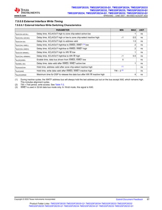
![7.10.4 Sequential Sampling Mode (Single-Channel) (SMODE = 0)
In sequential sampling mode, the ADC can continuously convert input signals on any of the channels (Ax to Bx).
The ADC can start conversions on event triggers from the ePWM, software trigger, or from an external ADCSOC
signal. If the SMODE bit is 0, the ADC will do conversions on the selected channel on every Sample/Hold pulse.
The conversion time and latency of the Result register update are explained below. The ADC interrupt flags are
set a few SYSCLKOUT cycles after the Result register update. The selected channels will be sampled at every
falling edge of the Sample/Hold pulse. The Sample/Hold pulse width can be programmed to be 1 ADC clock
wide (minimum) or 16 ADC clocks wide (maximum).
Analog Input on
Channel Ax or Bx
ADC Clock
Sample and Hold
SH Pulse
SMODE Bit
tdschx_n
tdschx_n+1
Sample n
Sample n+1
Sample n+2
tSH
ADC Event Trigger from
ePWM or Other Sources
td(SH)
Figure 7-39. Sequential Sampling Mode (Single-Channel) Timing
7.10.4.1 Sequential Sampling Mode Timing
SAMPLE n SAMPLE n + 1
AT 25-MHz
ADC CLOCK,
tc(ADCCLK) = 40 ns
REMARKS
td(SH)
Delay time from event trigger to
sampling
2.5tc(ADCCLK)
tSH
Sample/Hold width/Acquisition
Width
(1 + Acqps) *
tc(ADCCLK)
40 ns with Acqps = 0
Acqps value = 0-15
ADCTRL1[8:11]
td(schx_n)
Delay time for first result to appear
in Result register
4tc(ADCCLK) 160 ns
td(schx_n+1)
Delay time for successive results to
appear in Result register
(2 + Acqps) *
tc(ADCCLK)
80 ns
www.ti.com
TMS320F28335, TMS320F28335-Q1, TMS320F28334, TMS320F28333
TMS320F28332, TMS320F28235, TMS320F28235-Q1
TMS320F28234, TMS320F28234-Q1, TMS320F28232, TMS320F28232-Q1
SPRS439Q – JUNE 2007 – REVISED AUGUST 2022
Copyright © 2022 Texas Instruments Incorporated Submit Document Feedback 103
Product Folder Links: TMS320F28335 TMS320F28335-Q1 TMS320F28334 TMS320F28333 TMS320F28332
TMS320F28235 TMS320F28235-Q1 TMS320F28234 TMS320F28234-Q1 TMS320F28232 TMS320F28232-Q1](https://image.slidesharecdn.com/tms320f28335-231214074210-26d2911a/85/tms320f28335-pdf-103-320.jpg)
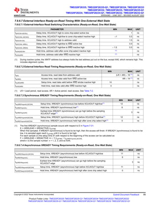
![7.10.5 Simultaneous Sampling Mode (Dual-Channel) (SMODE = 1)
In simultaneous mode, the ADC can continuously convert input signals on any one pair of channels (A0/B0 to
A7/B7). The ADC can start conversions on event triggers from the ePWM, software trigger, or from an external
ADCSOC signal. If the SMODE bit is 1, the ADC will do conversions on two selected channels on every Sample/
Hold pulse. The conversion time and latency of the result register update are explained below. The ADC interrupt
flags are set a few SYSCLKOUT cycles after the Result register update. The selected channels will be sampled
simultaneously at the falling edge of the Sample/Hold pulse. The Sample/Hold pulse width can be programmed
to be 1 ADC clock wide (minimum) or 16 ADC clocks wide (maximum).
Note
In simultaneous mode, the ADCIN channel pair select must be A0/B0, A1/B1, ..., A7/B7, and not in
other combinations (such as A1/B3, and so on).
Analog Input on
Channel Ax
Analog Input on
Channel Bx
ADC Clock
Sample and Hold
SH Pulse
tSH
tdschA0_n
tdschB0_n
tdschB0_n+1
Sample n
Sample n+1 Sample n+2
tdschA0_n+1
td(SH)
ADC Event Trigger from
ePWM or Other Sources
SMODE Bit
Figure 7-40. Simultaneous Sampling Mode Timing
7.10.5.1 Simultaneous Sampling Mode Timing
SAMPLE n SAMPLE n + 1
AT 25-MHz
ADC CLOCK,
tc(ADCCLK) = 40 ns
REMARKS
td(SH)
Delay time from event trigger to
sampling
2.5tc(ADCCLK)
tSH
Sample/Hold width/Acquisition
Width
(1 + Acqps) *
tc(ADCCLK)
40 ns with Acqps = 0
Acqps value = 0-15
ADCTRL1[8:11]
td(schA0_n)
Delay time for first result to
appear in Result register
4tc(ADCCLK) 160 ns
td(schB0_n )
Delay time for first result to
appear in Result register
5tc(ADCCLK) 200 ns
td(schA0_n+1)
Delay time for successive results
to appear in Result register
(3 + Acqps) * tc(ADCCLK) 120 ns
td(schB0_n+1 )
Delay time for successive results
to appear in Result register
(3 + Acqps) * tc(ADCCLK) 120 ns
TMS320F28335, TMS320F28335-Q1, TMS320F28334, TMS320F28333
TMS320F28332, TMS320F28235, TMS320F28235-Q1
TMS320F28234, TMS320F28234-Q1, TMS320F28232, TMS320F28232-Q1
SPRS439Q – JUNE 2007 – REVISED AUGUST 2022 www.ti.com
104 Submit Document Feedback Copyright © 2022 Texas Instruments Incorporated
Product Folder Links: TMS320F28335 TMS320F28335-Q1 TMS320F28334 TMS320F28333 TMS320F28332
TMS320F28235 TMS320F28235-Q1 TMS320F28234 TMS320F28234-Q1 TMS320F28232 TMS320F28232-Q1](https://image.slidesharecdn.com/tms320f28335-231214074210-26d2911a/85/tms320f28335-pdf-104-320.jpg)


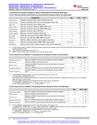
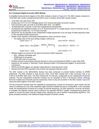
![ADC
RESULT
registers
ADC
CPU
PF0
I/F
ADC
DMA
PF0
I/F
ADC
control
and
RESULT
registers
ADC
PF2
I/F
L4
I/F
L4
SARAM
(4Kx16)
L5
I/F
L5
SARAM
(4Kx16)
L6
I/F
L6
SARAM
(4Kx16)
L7
I/F
L7
SARAM
(4Kx16)
PF3
I/F
McBSP A
McBSP B
Event
triggers
DMA
6-ch
External
interrupts
CPU
timers
CPU bus
DMA bus
PIE
INT7
DINT[CH1:CH6]
CPU
XINTF
zones
interface
XINTF
memory
zones
ePWM/
HRPWM
registers
(A)
A. The ePWM and HRPWM registers must be remapped to PF3 (through bit 0 of the MAPCNF register) before they can be accessed by
the DMA. The ePWM or HRPWM connection to DMA is not present in silicon revision 0.
Figure 8-1. DMA Functional Block Diagram
TMS320F28335, TMS320F28335-Q1, TMS320F28334, TMS320F28333
TMS320F28332, TMS320F28235, TMS320F28235-Q1
TMS320F28234, TMS320F28234-Q1, TMS320F28232, TMS320F28232-Q1
SPRS439Q – JUNE 2007 – REVISED AUGUST 2022 www.ti.com
116 Submit Document Feedback Copyright © 2022 Texas Instruments Incorporated
Product Folder Links: TMS320F28335 TMS320F28335-Q1 TMS320F28334 TMS320F28333 TMS320F28332
TMS320F28235 TMS320F28235-Q1 TMS320F28234 TMS320F28234-Q1 TMS320F28232 TMS320F28232-Q1](https://image.slidesharecdn.com/tms320f28335-231214074210-26d2911a/85/tms320f28335-pdf-116-320.jpg)
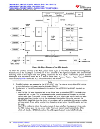
![CTR=PRD
TBPRD shadow (16)
TBPRD active (16)
Counter
up/down
(16 bit)
TBCTR
active (16)
TBCTL[PHSEN]
TBCTL[SWFSYNC]
(software forced sync)
EPWMxSYNCI
CTR=ZERO
CTR_Dir
CTR=CMPB
Disabled
Sync
in/out
select
Mux
TBCTL[SYNCOSEL]
EPWMxSYNCO
TBPHS active (24)
16 8
TBPHSHR (8)
Phase
control
Time−base (TB)
CTR=CMPA
CMPA active (24)
16
CMPA shadow (24)
Action
qualifier
(AQ)
8
16
Counter compare (CC)
CMPB active (16)
CTR=CMPB
CMPB shadow (16)
CMPAHR (8)
EPWMA
EPWMB
Dead
band
(DB) (PC)
chopper
PWM
zone
(TZ)
Trip
CTR = ZERO
EPWMxAO
EPWMxBO
EPWMxTZINT
TZ1 to TZ6
HRPWM
CTR = PRD
CTR = ZERO
CTR = CMPB
CTR = CMPA
CTR_Dir
Event
trigger
and
interrupt
(ET)
EPWMxINT
EPWMxSOCA
EPWMxSOCB
CTR=ZERO
Figure 8-5. ePWM Submodules Showing Critical Internal Signal Interconnections
8.2.4 High-Resolution PWM (HRPWM)
The HRPWM module offers PWM resolution (time granularity) which is significantly better than what can be
achieved using conventionally derived digital PWM methods. The key points for the HRPWM module are:
• Significantly extends the time resolution capabilities of conventionally derived digital PWM
• Typically used when effective PWM resolution falls below approximately 9 or 10 bits. This occurs at PWM
frequencies greater than approximately 200 kHz when using a CPU/System clock of 100 MHz.
• This capability can be used in both duty cycle and phase-shift control methods.
• Finer time granularity control or edge positioning is controlled through extensions to the Compare A and
Phase registers of the ePWM module.
• HRPWM capabilities are offered only on the A signal path of an ePWM module (that is, on the EPWMxA
output). EPWMxB output has conventional PWM capabilities.
TMS320F28335, TMS320F28335-Q1, TMS320F28334, TMS320F28333
TMS320F28332, TMS320F28235, TMS320F28235-Q1
TMS320F28234, TMS320F28234-Q1, TMS320F28232, TMS320F28232-Q1
SPRS439Q – JUNE 2007 – REVISED AUGUST 2022 www.ti.com
122 Submit Document Feedback Copyright © 2022 Texas Instruments Incorporated
Product Folder Links: TMS320F28335 TMS320F28335-Q1 TMS320F28334 TMS320F28333 TMS320F28332
TMS320F28235 TMS320F28235-Q1 TMS320F28234 TMS320F28234-Q1 TMS320F28232 TMS320F28232-Q1](https://image.slidesharecdn.com/tms320f28335-231214074210-26d2911a/85/tms320f28335-pdf-122-320.jpg)
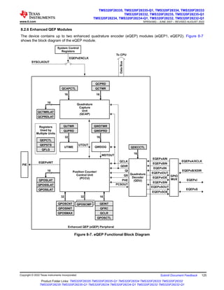
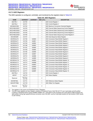
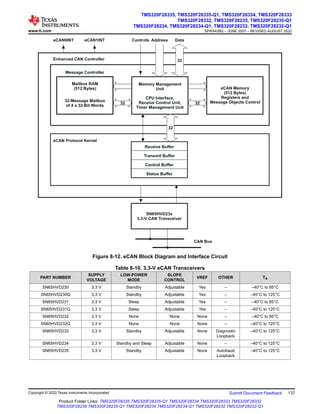
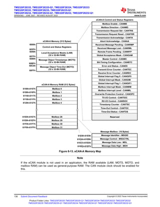
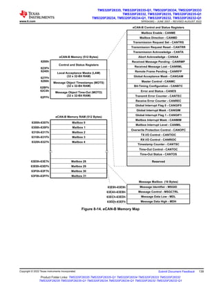
![8.2.5 Enhanced CAP Modules
The 2833x/2823x device contains up to six enhanced capture (eCAP) modules (eCAP1 to eCAP6). Figure 8-6
shows a functional block diagram of a module.
TSCTR
(Counter - 32-bit)
RST
CAP1
(APRD Active) LD
CAP2
(ACMP Active) LD
CAP3
(APRD Shadow) LD
CAP4
(ACMP Shadow) LD
Continuous/
One-Shot
Capture Control
LD1
LD2
LD3
LD4
32
PRD [0-31]
CTR [0-31]
eCAPx
MODE
SELECT
Interrupt
Trigger
and
Flag
Control
to PIE
CTR=CMP
32
32
32
ACMP
Shadow
Event
Prescale
CTRPHS
(Phase Register - 32-bit)
SYNCOut
SYNCIn
SYNC
Event
Qualifier
Polarity
Select
Polarity
Select
Polarity
Select
Polarity
Select
CTR=PRD
CTR_OVF
4
PWM
Compare
Logic
CTR [0-31]
PRD [0-31]
CMP [0-31]
CTR=CMP
CTR=PRD
CTR_OVF
OVF
APWM Mode
Delta Mode
4
Capture Events
CEVT[1:4]
APRD
Shadow
32
32
32
32
32
CMP [0-31]
Figure 8-6. eCAP Functional Block Diagram
www.ti.com
TMS320F28335, TMS320F28335-Q1, TMS320F28334, TMS320F28333
TMS320F28332, TMS320F28235, TMS320F28235-Q1
TMS320F28234, TMS320F28234-Q1, TMS320F28232, TMS320F28232-Q1
SPRS439Q – JUNE 2007 – REVISED AUGUST 2022
Copyright © 2022 Texas Instruments Incorporated Submit Document Feedback 123
Product Folder Links: TMS320F28335 TMS320F28335-Q1 TMS320F28334 TMS320F28333 TMS320F28332
TMS320F28235 TMS320F28235-Q1 TMS320F28234 TMS320F28234-Q1 TMS320F28232 TMS320F28232-Q1](https://image.slidesharecdn.com/tms320f28335-231214074210-26d2911a/85/tms320f28335-pdf-123-320.jpg)
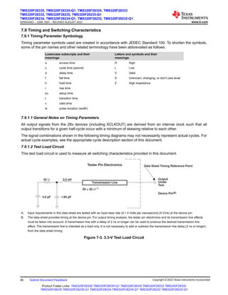
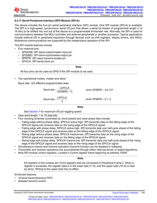
![Figure 8-9 shows the ADC pin-biasing for internal reference and Figure 8-10 shows the ADC pin-biasing for
external reference.
ADCINA[7:0]
ADCINB[7:0]
ADCLO
ADCREFIN
ADC External Current Bias Resistor ADCRESEXT
ADCREFP
VDD1A18
VDD2A18
VSS1AGND
VSS2AGND
VDDAIO
VSSAIO
VDDA2
VSSA2
ADC Reference Positive Output
ADCREFM
ADC Reference Medium Output
Reference I/O Power
Analog input 0−3 V with respect to ADCLO
Connect to analog ground
ADC Analog Power Pin (1.9 V/1.8 V)
ADC Analog Power Pin (1.9 V/1.8 V)
ADC Analog Power Pin (3.3 V)
ADC Analog I/O Ground Pin
ADC Analog Power Pin (3.3 V)
ADCREFP and ADCREFM should not
be loaded by external circuitry
ADC Analog Ground Pin
ADC 16-Channel Analog Inputs
Connect to analog ground if internal reference is used
ADC Analog Ground Pin
ADC Analog Ground Pin
22 k
2.2 F
μ
(A)
2.2 F
μ
(A)
A. TAIYO YUDEN LMK212BJ225MG-T or equivalent
B. External decoupling capacitors are recommended on all power pins.
C. Analog inputs must be driven from an operational amplifier that does not degrade the ADC performance.
Figure 8-9. ADC Pin Connections With Internal Reference
www.ti.com
TMS320F28335, TMS320F28335-Q1, TMS320F28334, TMS320F28333
TMS320F28332, TMS320F28235, TMS320F28235-Q1
TMS320F28234, TMS320F28234-Q1, TMS320F28232, TMS320F28232-Q1
SPRS439Q – JUNE 2007 – REVISED AUGUST 2022
Copyright © 2022 Texas Instruments Incorporated Submit Document Feedback 129
Product Folder Links: TMS320F28335 TMS320F28335-Q1 TMS320F28334 TMS320F28333 TMS320F28332
TMS320F28235 TMS320F28235-Q1 TMS320F28234 TMS320F28234-Q1 TMS320F28232 TMS320F28232-Q1](https://image.slidesharecdn.com/tms320f28335-231214074210-26d2911a/85/tms320f28335-pdf-129-320.jpg)
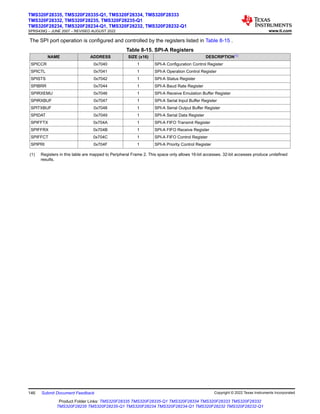
![ADCINA[7:0]
ADCINB[7:0]
ADCLO
ADCREFIN
ADC External Current Bias Resistor ADCRESEXT
ADCREFP
VDD1A18
VDD2A18
VSS1AGND
VSS2AGND
VDDAIO
VSSAIO
VDDA2
VSSA2
ADC Reference Positive Output
ADCREFM
ADC Reference Medium Output
Reference I/O Power
Analog input 0-3 V with respect to ADCLO
Connect to Analog Ground
ADCREFP and ADCREFM should not
be loaded by external circuitry
ADC 16-Channel Analog Inputs
Connect to 1.500, 1.024, or 2.048-V precision source
(D)
ADC Analog Power Pin (1.9 V/1.8 V)
ADC Analog Power Pin (1.9 V/1.8 V)
ADC Analog I/O Ground Pin
ADC Analog Power Pin (3.3 V)
ADC Analog Ground Pin
ADC Analog Ground Pin
ADC Analog Ground Pin
ADC Analog Power Pin (3.3 V)
22 k
2.2 F
μ
(A)
2.2 F
μ
(A)
A. TAIYO YUDEN LMK212BJ225MG-T or equivalent
B. External decoupling capacitors are recommended on all power pins.
C. Analog inputs must be driven from an operational amplifier that does not degrade the ADC performance.
D. External voltage on ADCREFIN is enabled by changing bits 15:14 in the ADC Reference Select register depending on the voltage used
on this pin. TI recommends TI part REF3020 or equivalent for 2.048-V generation. Overall gain accuracy will be determined by accuracy
of this voltage source.
Figure 8-10. ADC Pin Connections With External Reference
Note
The temperature rating of any recommended component must match the rating of the end product.
TMS320F28335, TMS320F28335-Q1, TMS320F28334, TMS320F28333
TMS320F28332, TMS320F28235, TMS320F28235-Q1
TMS320F28234, TMS320F28234-Q1, TMS320F28232, TMS320F28232-Q1
SPRS439Q – JUNE 2007 – REVISED AUGUST 2022 www.ti.com
130 Submit Document Feedback Copyright © 2022 Texas Instruments Incorporated
Product Folder Links: TMS320F28335 TMS320F28335-Q1 TMS320F28334 TMS320F28333 TMS320F28332
TMS320F28235 TMS320F28235-Q1 TMS320F28234 TMS320F28234-Q1 TMS320F28232 TMS320F28232-Q1](https://image.slidesharecdn.com/tms320f28335-231214074210-26d2911a/85/tms320f28335-pdf-130-320.jpg)

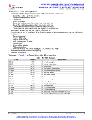
![8.2.12 Inter-Integrated Circuit (I2C)
The device contains one I2C Serial Port. Figure 8-17 shows how the I2C peripheral module interfaces within the
device.
SYSRS
SYSCLKOUT
Control
I2CINT1A
I2CINT2A
C28x CPU
GPIO
MUX
Peripheral
Bus
I2C-A
System Control Block
I2CAENCLK
PIE
Block
SDAA
SCLA
Data[16]
Data[16]
Addr[16]
A. The I2C registers are accessed at the SYSCLKOUT rate. The internal timing and signal waveforms of the I2C port are also at the
SYSCLKOUT rate.
B. The clock enable bit (I2CAENCLK) in the PCLKCR0 register turns off the clock to the I2C port for low power operation. Upon reset,
I2CAENCLK is clear, which indicates the peripheral internal clocks are off.
Figure 8-17. I2C Peripheral Module Interfaces
TMS320F28335, TMS320F28335-Q1, TMS320F28334, TMS320F28333
TMS320F28332, TMS320F28235, TMS320F28235-Q1
TMS320F28234, TMS320F28234-Q1, TMS320F28232, TMS320F28232-Q1
SPRS439Q – JUNE 2007 – REVISED AUGUST 2022 www.ti.com
148 Submit Document Feedback Copyright © 2022 Texas Instruments Incorporated
Product Folder Links: TMS320F28335 TMS320F28335-Q1 TMS320F28334 TMS320F28333 TMS320F28332
TMS320F28235 TMS320F28235-Q1 TMS320F28234 TMS320F28234-Q1 TMS320F28232 TMS320F28232-Q1](https://image.slidesharecdn.com/tms320f28335-231214074210-26d2911a/85/tms320f28335-pdf-148-320.jpg)

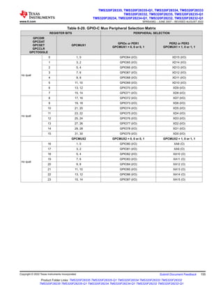
![8.2.14 External Interface (XINTF)
This section gives a top-level view of the external interface (XINTF) that is implemented on the 2833x/2823x
devices.
The XINTF is a nonmultiplexed asynchronous bus, similar to the 2812 XINTF. The XINTF is mapped into three
fixed zones shown in Figure 8-20.
XD[31:0]
XA[19:0]
XZCS0
XZCS6
XZCS7
XINTF Zone 0
(8K x 16)
0x0030-0000
0x0020-0000
0x0010-0000
0x0000-5000
0x0000-4000
0x0000-0000
Data Space Prog Space
XINTF Zone 6
(1M x 16)
XWE0
XR/W
XREADY
XHOLD
XHOLDA
XCLKOUT
XRD
XA0/XWE1
XINTF Zone 7
(1M x 16)
A. Each zone can be programmed with different wait states, setup and hold timings, and is supported by zone chip selects that toggle
when an access to a particular zone is performed. These features enable glueless connection to many external memories and
peripherals.
B. Zones 1 – 5 are reserved for future expansion.
C. Zones 0, 6, and 7 are always enabled.
Figure 8-20. External Interface Block Diagram
www.ti.com
TMS320F28335, TMS320F28335-Q1, TMS320F28334, TMS320F28333
TMS320F28332, TMS320F28235, TMS320F28235-Q1
TMS320F28234, TMS320F28234-Q1, TMS320F28232, TMS320F28232-Q1
SPRS439Q – JUNE 2007 – REVISED AUGUST 2022
Copyright © 2022 Texas Instruments Incorporated Submit Document Feedback 157
Product Folder Links: TMS320F28335 TMS320F28335-Q1 TMS320F28334 TMS320F28333 TMS320F28332
TMS320F28235 TMS320F28235-Q1 TMS320F28234 TMS320F28234-Q1 TMS320F28232 TMS320F28232-Q1](https://image.slidesharecdn.com/tms320f28335-231214074210-26d2911a/85/tms320f28335-pdf-157-320.jpg)
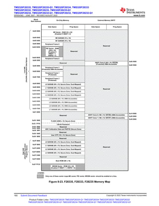
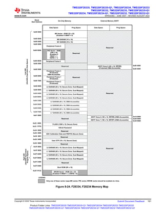
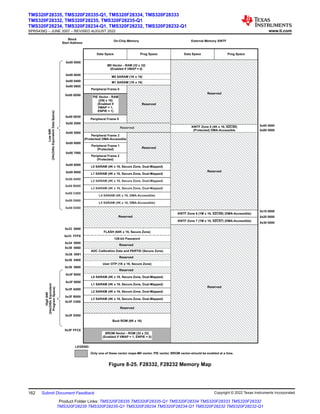
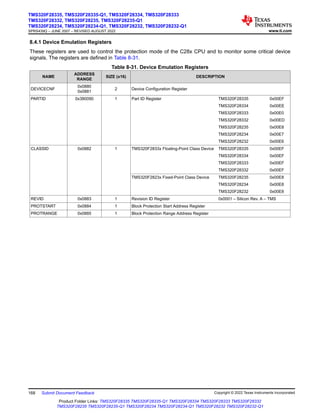
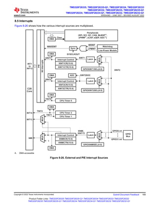
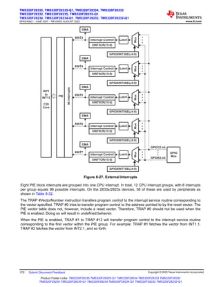
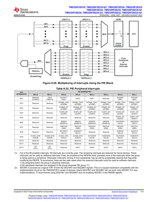
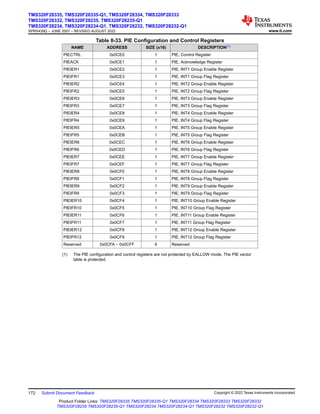
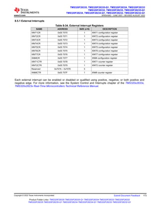
![8.6.1 OSC and PLL Block
Figure 8-30 shows the OSC and PLL block.
X1
XCLKIN
(3.3-V clock input
from external
oscillator)
On-chip
oscillator
X2
PLLSTS[OSCOFF]
OSCCLK
PLL
VCOCLK
4-bit Multiplier PLLCR[DIV]
OSCCLK or
VCOCLK CLKIN
OSCCLK
0
PLLSTS[PLLOFF]
n n ≠ 0
PLLSTS[DIVSEL]
/1
/2
/4
External
Crystal or
Resonator
To
CPU
Figure 8-30. OSC and PLL Block Diagram
The on-chip oscillator circuit enables a crystal/resonator to be attached to the 2833x/2823x devices using the X1
and X2 pins. If the on-chip oscillator is not used, an external oscillator can be used in either one of the following
configurations:
• A 3.3-V external oscillator can be directly connected to the XCLKIN pin. The X2 pin should be left
unconnected and the X1 pin tied low. The logic-high level in this case should not exceed VDDIO.
• A 1.9-V (1.8-V for 100 MHz devices) external oscillator can be directly connected to the X1 pin. The X2 pin
should be left unconnected and the XCLKIN pin tied low. The logic-high level in this case should not exceed
VDD.
The three possible input-clock configurations are shown in Figure 8-31 to Figure 8-33.
External Clock Signal
(Toggling 0-V )
DDIO
XCLKIN X2
NC
X1
Figure 8-31. Using a 3.3-V External Oscillator
External Clock Signal
(Toggling 0-V )
DD
XCLKIN X2
NC
X1
Figure 8-32. Using a 1.9-V External Oscillator
CL1
X2
X1
Crystal
CL2
XCLKIN
Figure 8-33. Using the Internal Oscillator
TMS320F28335, TMS320F28335-Q1, TMS320F28334, TMS320F28333
TMS320F28332, TMS320F28235, TMS320F28235-Q1
TMS320F28234, TMS320F28234-Q1, TMS320F28232, TMS320F28232-Q1
SPRS439Q – JUNE 2007 – REVISED AUGUST 2022 www.ti.com
176 Submit Document Feedback Copyright © 2022 Texas Instruments Incorporated
Product Folder Links: TMS320F28335 TMS320F28335-Q1 TMS320F28334 TMS320F28333 TMS320F28332
TMS320F28235 TMS320F28235-Q1 TMS320F28234 TMS320F28234-Q1 TMS320F28232 TMS320F28232-Q1](https://image.slidesharecdn.com/tms320f28335-231214074210-26d2911a/85/tms320f28335-pdf-176-320.jpg)
![8.6.1.1 External Reference Oscillator Clock Option
The typical specifications for the external quartz crystal for a frequency of 30 MHz follow:
• Fundamental mode, parallel resonant
• CL (load capacitance) = 12 pF
• CL1 = CL2 = 24 pF
• Cshunt = 6 pF
• ESR range = 25 to 40 Ω
TI recommends that customers have the resonator/crystal vendor characterize the operation of their device with
the MCU chip. The resonator/crystal vendor has the equipment and expertise to tune the tank circuit. The vendor
can also advise the customer regarding the proper tank component values that will produce proper start-up and
stability over the entire operating range.
8.6.1.2 PLL-Based Clock Module
The devices have an on-chip, PLL-based clock module. This module provides all the necessary clocking signals
for the device, as well as control for low-power mode entry. The PLL has a 4-bit ratio control PLLCR[DIV] to
select different CPU clock rates. The watchdog module should be disabled before writing to the PLLCR register.
It can be re-enabled (if need be) after the PLL module has stabilized, which takes 131072 OSCCLK cycles.
The input clock and PLLCR[DIV] bits should be chosen in such a way that the output frequency of the PLL
(VCOCLK) does not exceed 300 MHz.
Table 8-36. PLL Settings
PLLCR[DIV] VALUE(2) (3) PLLSTS[DIVSEL] = 0 or 1(1)
SYSCLKOUT (CLKIN)
PLLSTS[DIVSEL] = 2(1) PLLSTS[DIVSEL] = 3(1) (4)
0000 (PLL bypass) OSCCLK/4 (Default) OSCCLK/2 OSCCLK
0001 (OSCCLK * 1)/4 (OSCCLK * 1)/2 –
0010 (OSCCLK * 2)/4 (OSCCLK * 2)/2 –
0011 (OSCCLK * 3)/4 (OSCCLK * 3)/2 –
0100 (OSCCLK * 4)/4 (OSCCLK * 4)/2 –
0101 (OSCCLK * 5)/4 (OSCCLK * 5)/2 –
0110 (OSCCLK * 6)/4 (OSCCLK * 6)/2 –
0111 (OSCCLK * 7)/4 (OSCCLK * 7)/2 –
1000 (OSCCLK * 8)/4 (OSCCLK * 8)/2 –
1001 (OSCCLK * 9)/4 (OSCCLK * 9)/2 –
1010 (OSCCLK * 10)/4 (OSCCLK * 10)/2 –
1011 – 1111 Reserved Reserved Reserved
(1) By default, PLLSTS[DIVSEL] is configured for /4. (The boot ROM changes this to /2.) PLLSTS[DIVSEL] must be 0 before writing to the
PLLCR and should be changed only after PLLSTS[PLLLOCKS] = 1.
(2) The PLL control register (PLLCR) and PLL Status Register (PLLSTS) are reset to their default state by the XRS signal or a watchdog
reset only. A reset issued by the debugger or the missing clock detect logic have no effect.
(3) This register is EALLOW protected. See the System Control and Interrupts chapter of the TMS320x2833x, TMS320x2823x Real-Time
Microcontrollers Technical Reference Manual for more information.
(4) A divider at the output of the PLL is necessary to ensure correct duty cycle of the clock fed to the core. For this reason, a DIVSEL
value of 3 is not allowed when the PLL is active.
www.ti.com
TMS320F28335, TMS320F28335-Q1, TMS320F28334, TMS320F28333
TMS320F28332, TMS320F28235, TMS320F28235-Q1
TMS320F28234, TMS320F28234-Q1, TMS320F28232, TMS320F28232-Q1
SPRS439Q – JUNE 2007 – REVISED AUGUST 2022
Copyright © 2022 Texas Instruments Incorporated Submit Document Feedback 177
Product Folder Links: TMS320F28335 TMS320F28335-Q1 TMS320F28334 TMS320F28333 TMS320F28332
TMS320F28235 TMS320F28235-Q1 TMS320F28234 TMS320F28234-Q1 TMS320F28232 TMS320F28232-Q1](https://image.slidesharecdn.com/tms320f28335-231214074210-26d2911a/85/tms320f28335-pdf-177-320.jpg)
![Table 8-37. CLKIN Divide Options
PLLSTS [DIVSEL] CLKIN DIVIDE
0 /4
1 /4
2 /2
3 /1(1)
(1) This mode can be used only when the PLL is bypassed or off.
The PLL-based clock module provides two modes of operation:
• Crystal-operation - This mode allows the use of an external crystal/resonator to provide the time base to the
device.
• External clock source operation - This mode allows the internal oscillator to be bypassed. The device clocks
are generated from an external clock source input on the X1 or the XCLKIN pin.
Table 8-38. Possible PLL Configuration Modes
PLL MODE REMARKS PLLSTS[DIVSEL]
CLKIN AND
SYSCLKOUT
PLL Off
Invoked by the user setting the PLLOFF bit in the PLLSTS register. The PLL block
is disabled in this mode. This can be useful to reduce system noise and for low
power operation. The PLLCR register must first be set to 0x0000 (PLL Bypass)
before entering this mode. The CPU clock (CLKIN) is derived directly from the
input clock on either X1/X2, X1 or XCLKIN.
0, 1
2
3
OSCCLK/4
OSCCLK/2
OSCCLK/1
PLL Bypass
PLL Bypass is the default PLL configuration upon power up or after an external
reset ( XRS). This mode is selected when the PLLCR register is set to 0x0000
or while the PLL locks to a new frequency after the PLLCR register has been
modified. In this mode, the PLL itself is bypassed but the PLL is not turned off.
0, 1
2
3
OSCCLK/4
OSCCLK/2
OSCCLK/1
PLL Enable
Achieved by writing a nonzero value n into the PLLCR register. Upon writing to the
PLLCR the device will switch to PLL Bypass mode until the PLL locks.
0, 1
2
OSCCLK*n/4
OSCCLK*n/2
8.6.1.3 Loss of Input Clock
In PLL-enabled and PLL-bypass mode, if the input clock OSCCLK is removed or absent, the PLL will still issue
a limp-mode clock. The limp-mode clock continues to clock the CPU and peripherals at a typical frequency of
1–5 MHz. Limp mode is not specified to work from power up, only after input clocks have been present initially.
In PLL bypass mode, the limp mode clock from the PLL is automatically routed to the CPU if the input clock is
removed or absent.
Normally, when the input clocks are present, the watchdog counter decrements to initiate a watchdog reset or
WDINT interrupt. However, when the external input clock fails, the watchdog counter stops decrementing (that
is, the watchdog counter does not change with the limp-mode clock). In addition to this, the device will be reset
and the “Missing Clock Status” (MCLKSTS) bit will be set. These conditions could be used by the application
firmware to detect the input clock failure and initiate necessary shut-down procedure for the system.
Note
Applications in which the correct CPU operating frequency is absolutely critical should implement a
mechanism by which the MCU will be held in reset, should the input clocks ever fail. For example,
an R-C circuit may be used to trigger the XRS pin of the MCU, should the capacitor ever get fully
charged. An I/O pin may be used to discharge the capacitor on a periodic basis to prevent it from
getting fully charged. Such a circuit would also help detect failure of the flash memory and the VDD3VFL
rail.
TMS320F28335, TMS320F28335-Q1, TMS320F28334, TMS320F28333
TMS320F28332, TMS320F28235, TMS320F28235-Q1
TMS320F28234, TMS320F28234-Q1, TMS320F28232, TMS320F28232-Q1
SPRS439Q – JUNE 2007 – REVISED AUGUST 2022 www.ti.com
178 Submit Document Feedback Copyright © 2022 Texas Instruments Incorporated
Product Folder Links: TMS320F28335 TMS320F28335-Q1 TMS320F28334 TMS320F28333 TMS320F28332
TMS320F28235 TMS320F28235-Q1 TMS320F28234 TMS320F28234-Q1 TMS320F28232 TMS320F28232-Q1](https://image.slidesharecdn.com/tms320f28335-231214074210-26d2911a/85/tms320f28335-pdf-178-320.jpg)
![8.6.2 Watchdog Block
The watchdog block on the 2833x/2823x device is similar to the one used on the 240x and 281x devices.
The watchdog module generates an output pulse, 512 oscillator clocks wide (OSCCLK), whenever the 8-bit
watchdog up counter has reached its maximum value. To prevent this, the user disables the counter or the
software must periodically write a 0x55 + 0xAA sequence into the watchdog key register which will reset the
watchdog counter. Figure 8-34 shows the various functional blocks within the watchdog module.
/512
OSCCLK
WDCR (WDPS[2:0])
WDCLK
SCSR(WDOVERRIDE)
WDCNTR(7:0)
WDKEY(7:0)
Good K ey
1 0 1
WDCR (WDCHK[2:0])
Bad
WDCHK
Key
WDCR (WDDIS)
Clear Counter
SCSR (WDENINT)
Watchdog
Prescaler
Generate
Output Pulse
(512 OSCCLKs)
8-Bit
Watchdog
Counter
CLR
WDRST
WDINT
Watchdog
55 + AA
Key Detector
Core-reset
XRS
WDRST(A)
Internal
Pullup
A. The WDRST signal is driven low for 512 OSCCLK cycles.
Figure 8-34. Watchdog Module
The WDINT signal enables the watchdog to be used as a wakeup from IDLE/STANDBY mode.
In STANDBY mode, all peripherals are turned off on the device. The only peripheral that remains functional is
the watchdog. The WATCHDOG module will run off OSCCLK. The WDINT signal is fed to the LPM block so that
it can wake the device from STANDBY (if enabled). See Section 8.7, Low-Power Modes Block, for more details.
In IDLE mode, the WDINT signal can generate an interrupt to the CPU, through the PIE, to take the CPU out of
IDLE mode.
In HALT mode, this feature cannot be used because the oscillator (and PLL) are turned off and hence so is the
WATCHDOG.
www.ti.com
TMS320F28335, TMS320F28335-Q1, TMS320F28334, TMS320F28333
TMS320F28332, TMS320F28235, TMS320F28235-Q1
TMS320F28234, TMS320F28234-Q1, TMS320F28232, TMS320F28232-Q1
SPRS439Q – JUNE 2007 – REVISED AUGUST 2022
Copyright © 2022 Texas Instruments Incorporated Submit Document Feedback 179
Product Folder Links: TMS320F28335 TMS320F28335-Q1 TMS320F28334 TMS320F28333 TMS320F28332
TMS320F28235 TMS320F28235-Q1 TMS320F28234 TMS320F28234-Q1 TMS320F28232 TMS320F28232-Q1](https://image.slidesharecdn.com/tms320f28335-231214074210-26d2911a/85/tms320f28335-pdf-179-320.jpg)
![8.7 Low-Power Modes Block
The low-power modes on the 2833x/2823x devices are similar to the 240x devices. Table 8-39 summarizes the
various modes.
Table 8-39. Low-Power Modes
MODE LPMCR0(1:0) OSCCLK CLKIN SYSCLKOUT EXIT(1)
IDLE 00 On On On(2) XRS, watchdog interrupt, any enabled
interrupt, XNMI
STANDBY 01
On
(watchdog still running)
Off Off
XRS, watchdog interrupt, GPIO Port A
signal, debugger(3), XNMI
HALT 1X
Off
(oscillator and PLL turned off,
watchdog not functional)
Off Off
XRS, GPIO port A signal, XNMI,
debugger(3)
(1) The EXIT column lists which signals or under what conditions the low-power mode will be exited. A low signal, on any of the signals,
will exit the low power condition. This signal must be kept low long enough for an interrupt to be recognized by the device. Otherwise,
the IDLE mode will not be exited and the device will go back into the indicated low-power mode.
(2) The IDLE mode on the C28x behaves differently than on the 24x/240x. On the C28x, the clock output from the CPU (SYSCLKOUT) is
still functional while on the 24x/240x the clock is turned off.
(3) On the C28x, the JTAG port can still function even if the CPU clock (CLKIN) is turned off.
The various low-power modes operate as follows:
IDLE mode: This mode is exited by any enabled interrupt or an XNMI that is recognized by
the processor. The LPM block performs no tasks during this mode as long as the
LPMCR0(LPM) bits are set to 0,0.
STANDBY mode: Any GPIO port A signal (GPIO[31:0]) can wake the device from STANDBY mode.
The user must select which signal(s) will wake the device in the GPIOLPMSEL
register. The selected signal(s) are also qualified by the OSCCLK before waking
the device. The number of OSCCLKs is specified in the LPMCR0 register.
HALT mode: Only the XRS and any GPIO port A signal (GPIO[31:0]) can wake the device from
HALT mode. The user selects the signal in the GPIOLPMSEL register.
Note
The low-power modes do not affect the state of the output pins (PWM pins included). They will be in
whatever state the code left them in when the IDLE instruction was executed. See the System Control
and Interrupts chapter of the TMS320x2833x, TMS320x2823x Real-Time Microcontrollers Technical
Reference Manual for more details.
TMS320F28335, TMS320F28335-Q1, TMS320F28334, TMS320F28333
TMS320F28332, TMS320F28235, TMS320F28235-Q1
TMS320F28234, TMS320F28234-Q1, TMS320F28232, TMS320F28232-Q1
SPRS439Q – JUNE 2007 – REVISED AUGUST 2022 www.ti.com
180 Submit Document Feedback Copyright © 2022 Texas Instruments Incorporated
Product Folder Links: TMS320F28335 TMS320F28335-Q1 TMS320F28334 TMS320F28333 TMS320F28332
TMS320F28235 TMS320F28235-Q1 TMS320F28234 TMS320F28234-Q1 TMS320F28232 TMS320F28232-Q1](https://image.slidesharecdn.com/tms320f28335-231214074210-26d2911a/85/tms320f28335-pdf-180-320.jpg)


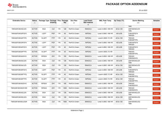
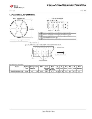

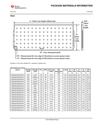
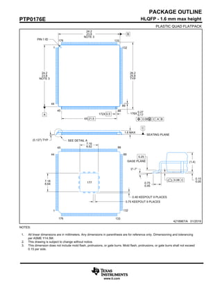
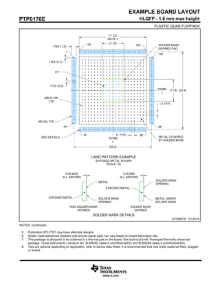
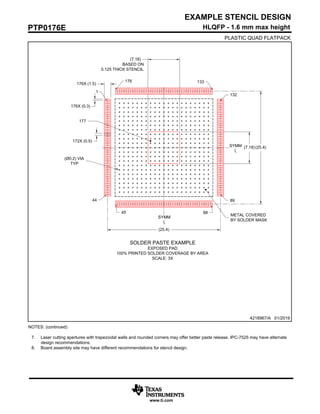
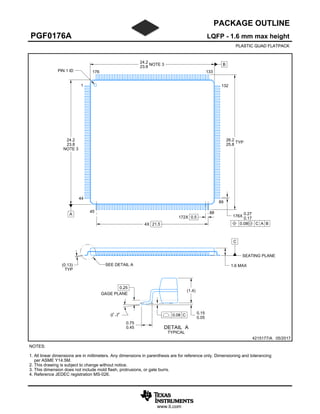
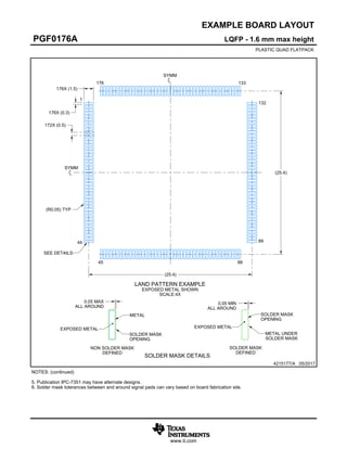
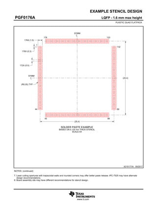
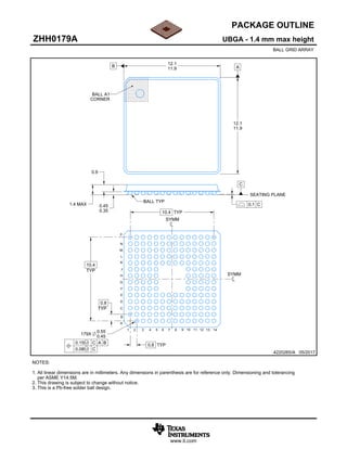
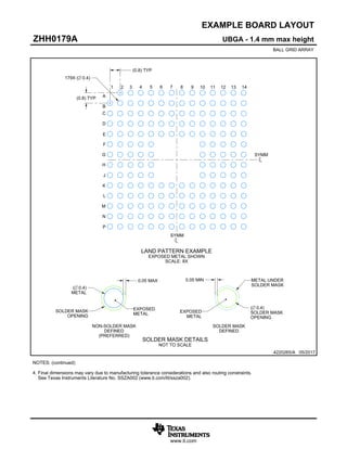
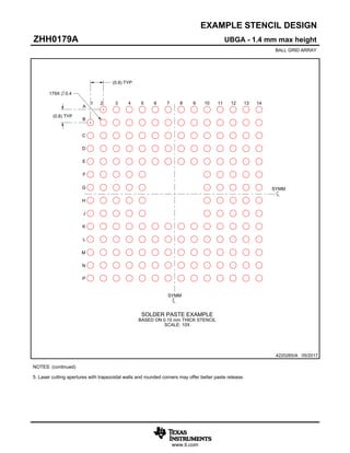
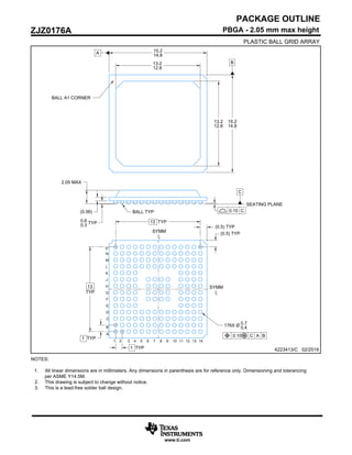
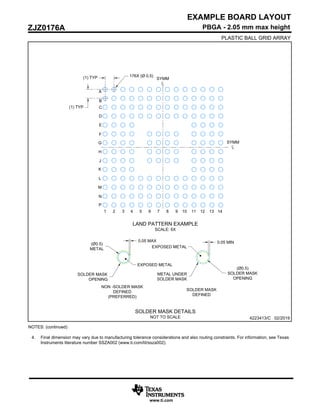
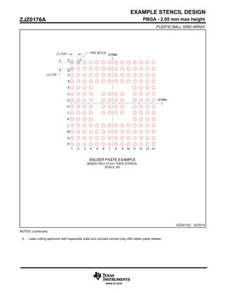
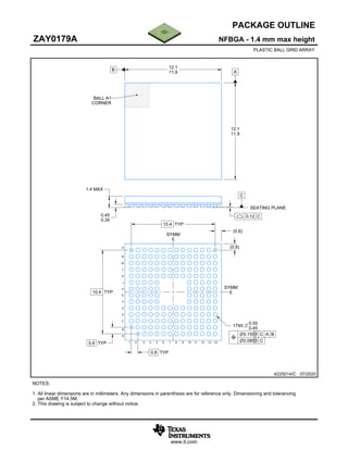
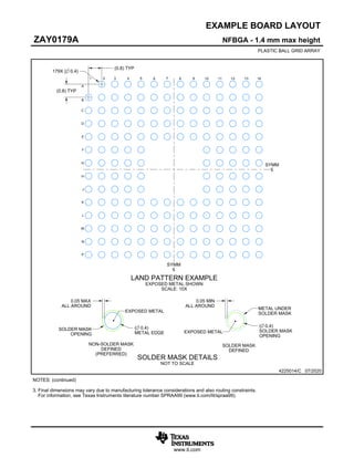
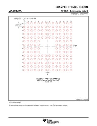


The TMS320F2833x and TMS320F2823x real-time microcontrollers feature a high-performance 32-bit CPU, multiple peripheral interfaces, and advanced control peripherals, making them suitable for demanding applications like motor control and power delivery. They include extensive memory options, a built-in ADC, and a variety of package options while supporting various power modes to enhance energy efficiency. These devices are optimized for real-time processing and are targeted for applications such as advanced driver assistance systems and factory automation.


![Getting Started with Apache Spark: Big Data Made Simple [Free Meetup]](https://cdn.slidesharecdn.com/ss_thumbnails/apachesparkgettingstarted-260203175547-8361bcc3-thumbnail.jpg?width=640&height=640&fit=bounds)


