![Input Filters
6
Differential-mode signal –3 dB cutoff frequency ,
fDIF = 1 / [2π · (RF1 + RF2) · (CDIF1 + CCM1|| CCM2)] ≈ 3.4K Hz
Common-mode signal –3 dB cutoff frequency ,
fCM = 1 / (2π · RF1 · CCM1) = 1 / (2π · RF2 · CCM2) ≈ 34M Hz](https://image.slidesharecdn.com/thearchitectureofvenusdataacquisitionsystemforwaqmproject-200820142114/75/The-architecture-of-venus-data-acquisition-system-for-waqm-project-6-2048.jpg)
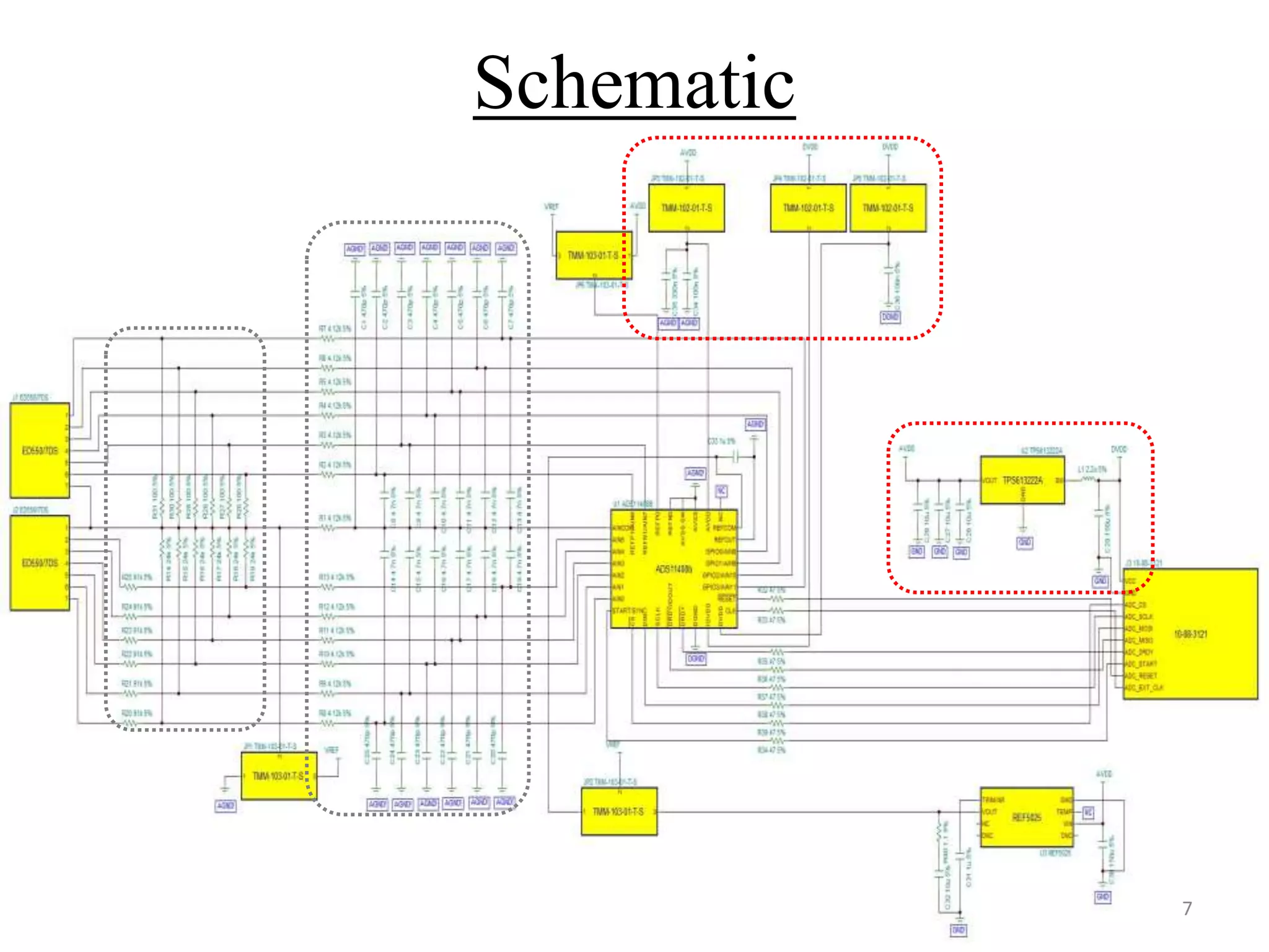
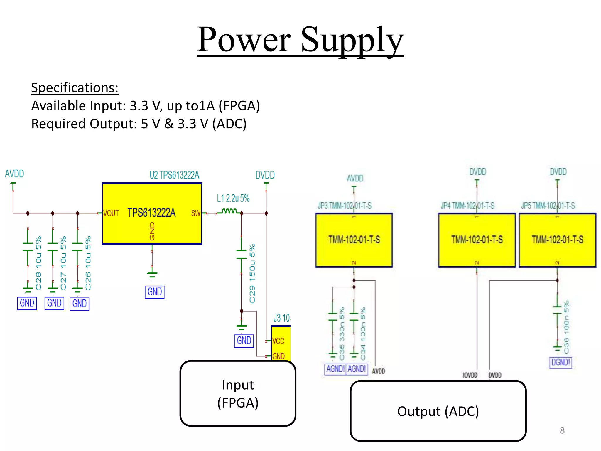
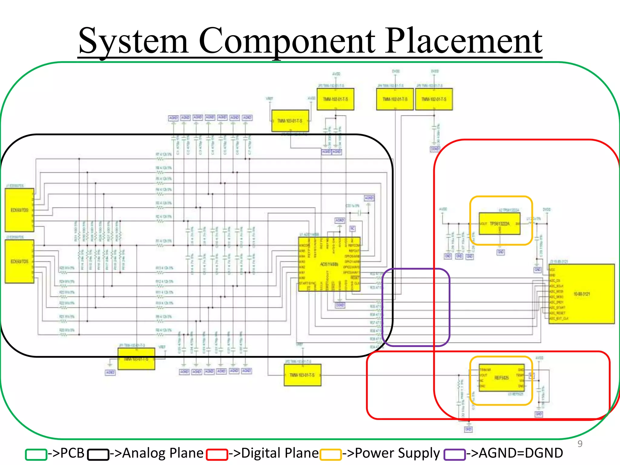


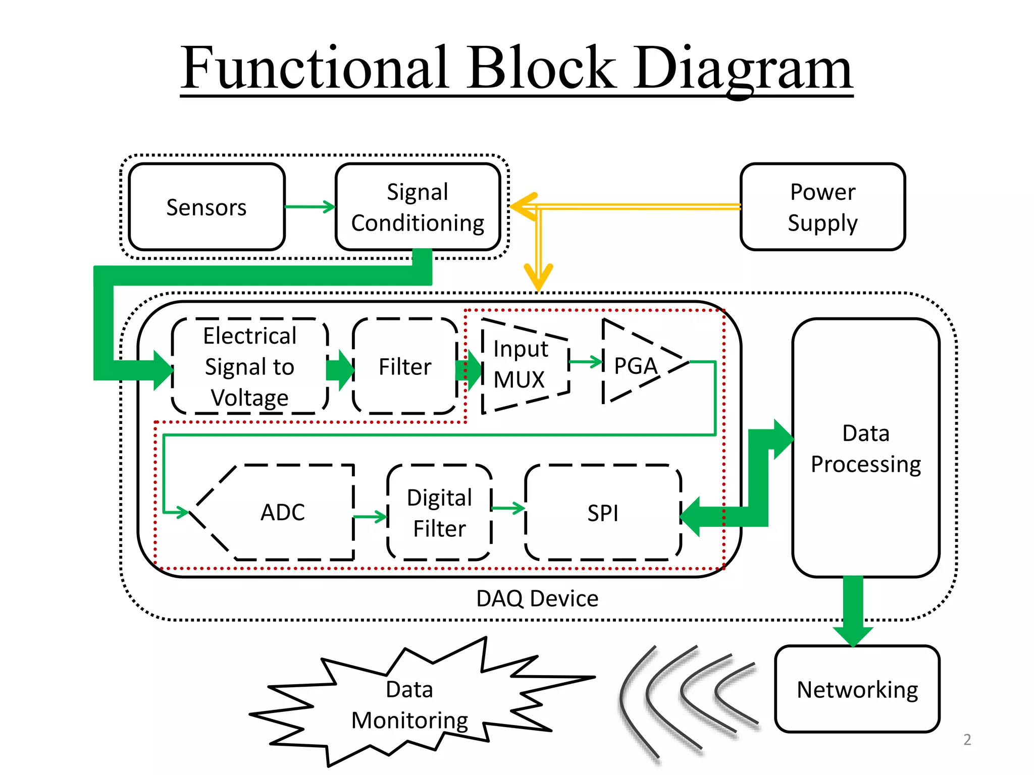
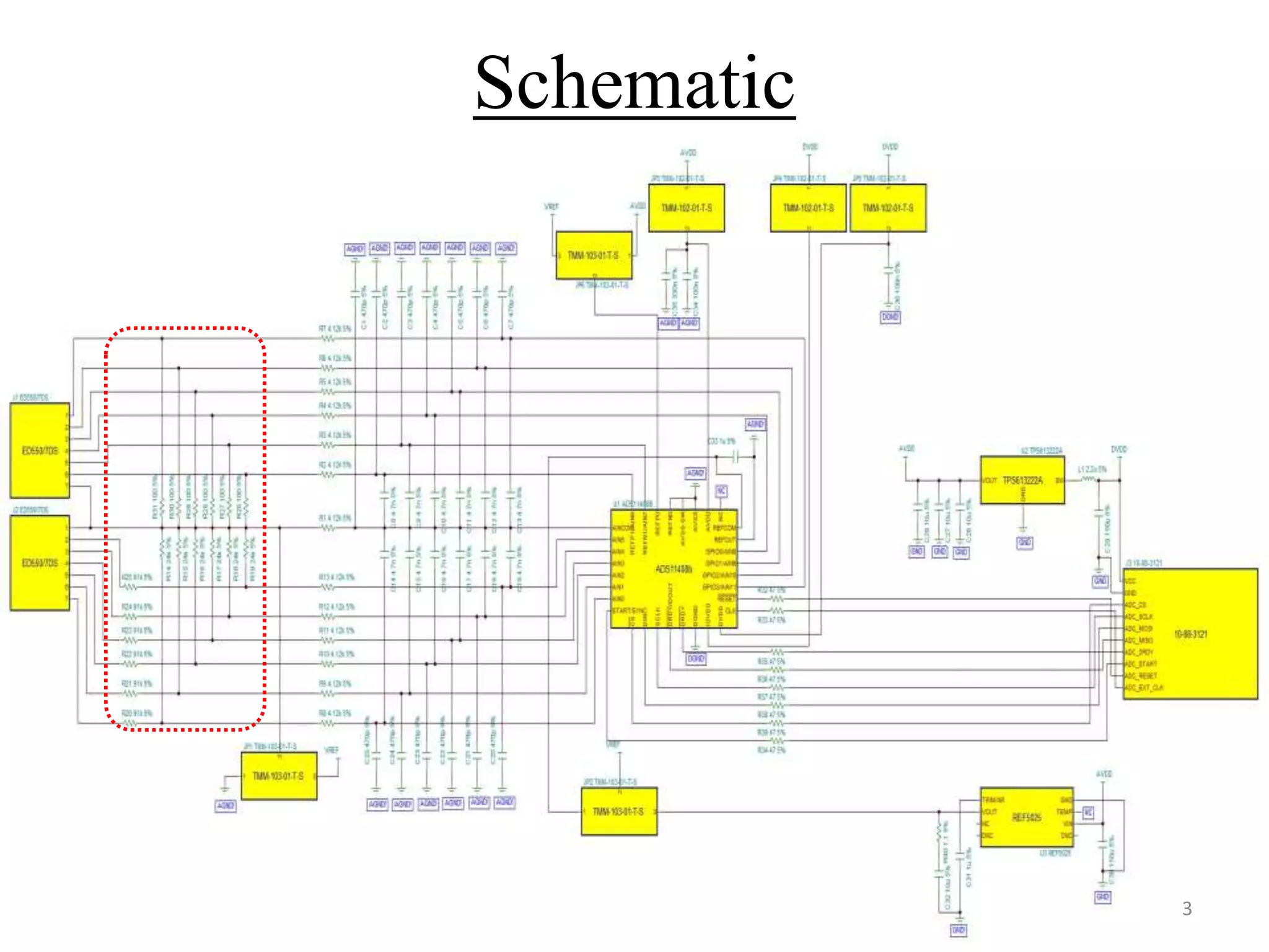
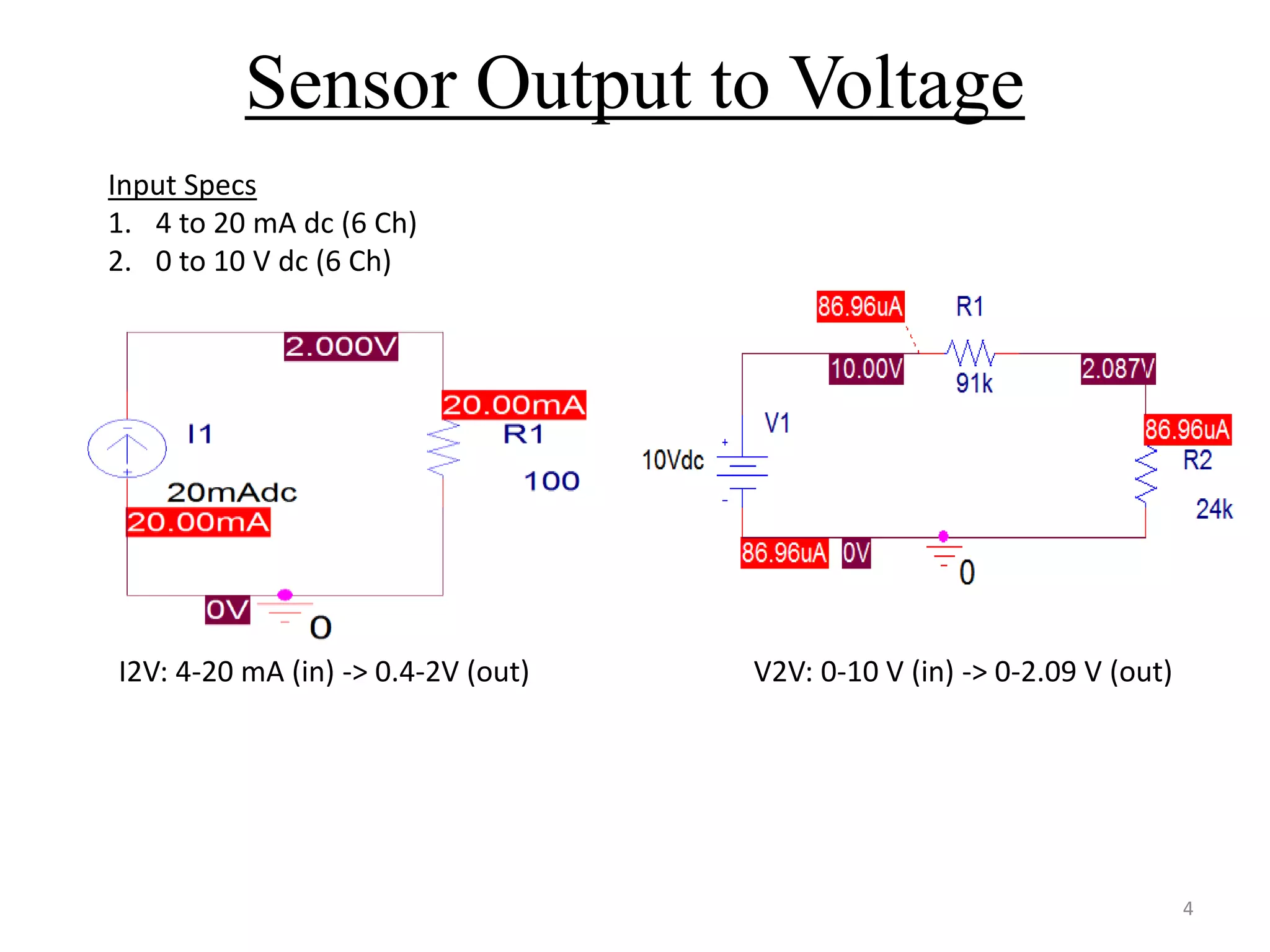
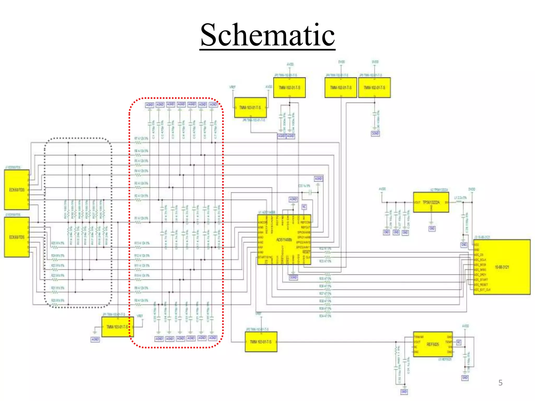
The document details the architecture of the Venus data acquisition system for the WAQM project, outlining its functional blocks, including sensors, signal conditioning, and data processing. Key specifications and signal outputs are provided, including input/output voltage ranges and cutoff frequencies for differential and common-mode signals. Additionally, it includes power supply requirements and system component placement within the PCB layout.


![Vibe Coding vs. Spec-Driven Development [Free Meetup]](https://cdn.slidesharecdn.com/ss_thumbnails/vibecodingvsspecdrivendevelopment-251209105622-43f455e7-thumbnail.jpg?width=640&height=640&fit=bounds)


