2. 073104-2 Mazumder et al. Appl. Phys. Lett. 97, 073104 2010
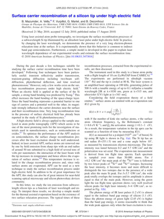
FIG. 2. Color online a Representation of tip geometries; b excitation
and two steps recombination processes; c simulated normalized evapora-
tion rate as function of time obtained for a Si tip with IR laser light and d
with green laser light. Different curves correspond to different carrier den-
sities N2 = 2 1020 cm−3, N2 = 8 1020 cm−3, N2 = 1021 cm−3, N2 = 3
1021 cm−3, and N2 = 7 1021 cm−3 bottom to top , respectively.
direction and it follows a Gaussian shape along the tip axis
direction with a typical width w. After the interaction with
FIG. 1. Color online Normalized evaporation rate as function of time the laser beam, electrons excited in the conduction band car-
obtained from an Si tip a for IR laser, using the laser intensities bottom to rier density N2 can relax their energy by a rapid recombina-
top I = 0.2 GW/ cm2, I = 1.2 GW/ cm2, I = 2.2 GW/ cm2, and I = 5.7 GW/ tion process due to electron-electron thermalization in the
cm2, respectively; b green laser light, smooth thick line corresponds to the conduction band intraband relaxation with typical time
best fit using Eq. 4 .
2 : dN2 / dt = −N2 / 2 and a long recombination process due
to interband electron-hole recombination with a typical time
nant with the band gap energy. To test this hypothesis and 1 : dN1 / dt = −N1 / 1 + N2 / 2, where N1 is the carrier density
also to check if this wavelength dependence is typical of in the bottom of the conduction band as schematically shown
silicon or can be extended to any indirect band gap semicon- in Fig. 2 b .13 We suppose that their energy is locally trans-
ductors, same experiments was conducted on silicon carbide ferred to the lattice by phonons excitation, leading to a tem-
SiC . The band gap energy of SiC is 2.36 eV, i.e., close to perature increase, so that the spatial and temporal heat evo-
the green photon energy 2.45 eV . The same behavior ob- lution takes place following the Fourier equation:
served for Si tip with IR green light was observed on SiC d
using green UV light. The same behavior was observed on G z,t dV = CV T t T t dV + − D T S+ z Tz
dt
a n-doped 51018 cm−3 of phosphorus and intrinsic Si tip,
showing that at T = 80 K the role of doping is negligible, as − S− z Tz , 2
expected.
where G z , t is the generation rate related to the recombina-
Considering the evaporation rate as a measure of the tip
tion process by
temperature variation, the presence of two peaks one narrow
and one wide , at high intensity for IR illumination, corre- N2 z,t N1 z,t
sponds to two heating processes delayed by several nanosec- G z,t = E2 + E1 , 3
2 1
ond. The temperature increase is related to the excitation of
charges and their recombination. Due to the long optical pen- where CV and D T are the volume specific heat and the
etration depth of Si at = 1030 nm 1 m Ref. 12 thermal conductivity of the Si tip, respectively. The values
and the small transverse dimensions of the tip D = 2R of CV and D T are reported in the literature for Si
= 100 nm , the laser excitation is uniform in the transverse nanowires,14,15 whose geometry is close to our tip geometry.
Downloaded 18 Aug 2010 to 193.52.145.137. Redistribution subject to AIP license or copyright; see http://apl.aip.org/about/rights_and_permissions
3. 073104-3 Mazumder et al. Appl. Phys. Lett. 97, 073104 2010
Taking into account the tip shape, S+ z and S− z correspond Another important parameter of our model is the long
to surfaces perpendicular to the tip axis delimiting the el- recombination time 1 = 20 ns which is very long as com-
emental volume dV, as represented in Fig. 2 a . The tempera- pared to the Auger recombination time for a charge density
ture evolution at the tip apex T z = 0 , t , predicted by this of 1021 cm−3 Auger a few picosecond .18 However, a sub-
simple model, can be introduced in Eq. 1 to check the stantial part of the photogenerated holes is swept toward the
evaporation rate dependence as a function of energy and la- surface by the strong near surface electric field and rapidly
ser wavelength. The activation energy Qn in Eq. 1 was captured by the surface states. On the other hand, the photo-
fixed at 0.1 eV as reported by Thompson et al.16 generated electrons are rapidly swept toward the bulk. Due
The carrier density N2 and the size of the excited zone to this spatial charge separation, the value of the charge
w were deduced from experimental data as follow. Consid- density for Auger calculation should be as follows:
ering the tip as a semi-infinite cylinder hot wire model ,8 N2Vholes / Velectrons = N210−3, taking into account the effective
with Tmax, the maximal temperature reached after the laser volume occupied by holes Vholes R2h with h = 0.4 nm the
4
illumination, the cooling rate is governed by band bending depth and by electrons Velectrons R 2w .
Tmax As a conclusion, we studied the evaporation of a Si tip as
Tt . 4 a function of the laser wavelength and intensity using laser
2D assisted APT. We showed that it is possible to find a resonant
1+ 2 t
w laser wavelength for which a long evaporation process is
observed. We propose a model to explain this behavior tak-
Injecting Eq. 4 into Eq. 1 , this formula can be used to fit
ing into account the long recombination process of excited
the experimental behavior of the evaporation rate, as re-
charges at the surface of the tip under a high electric field.
ported in Fig. 1 b , with the fit parameters; Tmax = 180 K and
These results may be of significant importance for all people
w = 300 nm. Due to the energy conservation CV Tmax − T0
studying Si component for photovoltaic applications.
= N2 E2 + E1 , a temperature increase of 100 K corresponds
At last, our simple model allows an estimate of this sur-
to a charge density of N2 = 1021 cm−3, each charge transfer-
face recombination time and it explains well the role of the
ring an energy of E2 + E1 = 1.2 eV to the bulk.
laser wavelength on the evaporation process.
We fix the fast recombination time 2 = 2 ps as reported
in Ref. 13 and adjust the value of 1 at 20 ns to obtain a 1
J. Linnros, J. Appl. Phys. 84, 284 1998 .
delay between the two simulated peaks of 7 ns as experimen- 2
A. Sabbah and D. Riffe, Phys. Rev. B 66, 165217 2002 .
tally observed. As shown in Figs. 2 c and 2 d our simple 3
J. Long, H. Sadeghi, J. Rife, and M. Kabler, Phys. Rev. Lett. 64, 1158
model predicts well the experimental behavior. However 4
1990 .
some of these parameters need to be discussed. Considering T. Tsong, Surf. Sci. 85, 1 1979 .
5
L. Kronik and Y. Shapira, Surf. Sci. Rep. 37, 1 1999 .
the absorption coefficient of Si at = 1030 nm 6
M. Müller, A. Cerezo, G. Smith, L. Chang, and S. Gerstl, Appl. Phys. Lett.
= 10 cm−1 at 80 K,12 we obtain for the highest laser inten- 92, 233115 2008 .
sity a carrier density of 1017 cm−3, which is lower than the 7
T. Kelly and M. Miller, Rev. Sci. Instrum. 78, 031101 2007 .
8
value used for simulations. Taking into account the strong F. Vurpillot, J. Houard, A. Vella, and B. Deconihout, J. Phys. D: Appl.
Phys. 42, 125502 2009 .
band bending due to the high electric field at the tip surface, 9
A. Cerezo, G. Smith, and P. Clifton, Appl. Phys. Lett. 88, 154103 2006 .
a strong enhancement of absorption is expected. As predicted 10
B. Gault, F. Vurpillot, A. Vella, A. Bostel, A. Menand, and B. Deconihout,
by Tsong,4,11 in the tip geometries, this phenomenon can Rev. Sci. Instrum. 77, 043705 2006 .
11
heavily invert the surface, which becomes similar to a semi- M. Miller, A. Cerezo, M. Hetherington, and G. Smith, Atom Probe Field
metal surface with a surface holes density of 1021 cm−3. This Ion Microscopy Oxford Science Publication/Oxford University Press, Ox-
ford, 1996 .
is the reason why n-doped, p-doped, and intrinsic silicon 12
W. Dash and R. Newman, Phys. Rev. 99, 1151 1955 .
show the same experimental behavior. 13
A. Othonos, J. Appl. Phys. 83, 1789 1998 .
Moreover, we use for the size of excitation zone the 14
M. Omar and H. Taha, Physica B 404, 5203 2009 .
15
value of w = 300 nm, which is smaller than the laser spot on D. Li, Y. Wu, P. Kim, L. Shi, P. Yang, and A. Majumdar, Appl. Phys. Lett.
the tip about 50 m . If, due to the band bending, the ab- 83, 2934 2003 .
16
sorption properties of the Si surface are similar to those of a K. Thompson, D. Larson, and T. Kelly, Microsc. Microanal. 11, 888
2005 .
metal surface, this focalization of the absorption on a very 17
J. Houard, A. Vella, F. Vurpillot, and B. Deconihout, Phys. Rev. B 81,
small zone was already reported by authors17 and corre- 125411 2010 .
18
sponds to the light diffraction at the tip apex. D. Laks, G. Neumark, and S. Pantelides, Phys. Rev. B 42, 5176 1990 .
Downloaded 18 Aug 2010 to 193.52.145.137. Redistribution subject to AIP license or copyright; see http://apl.aip.org/about/rights_and_permissions