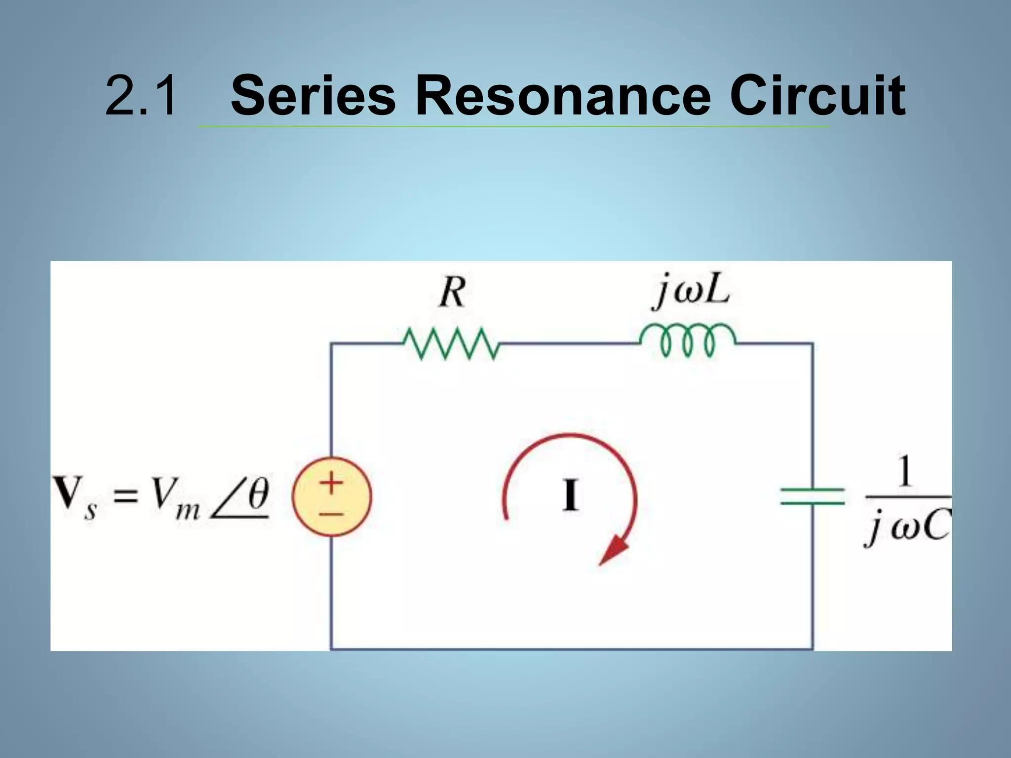
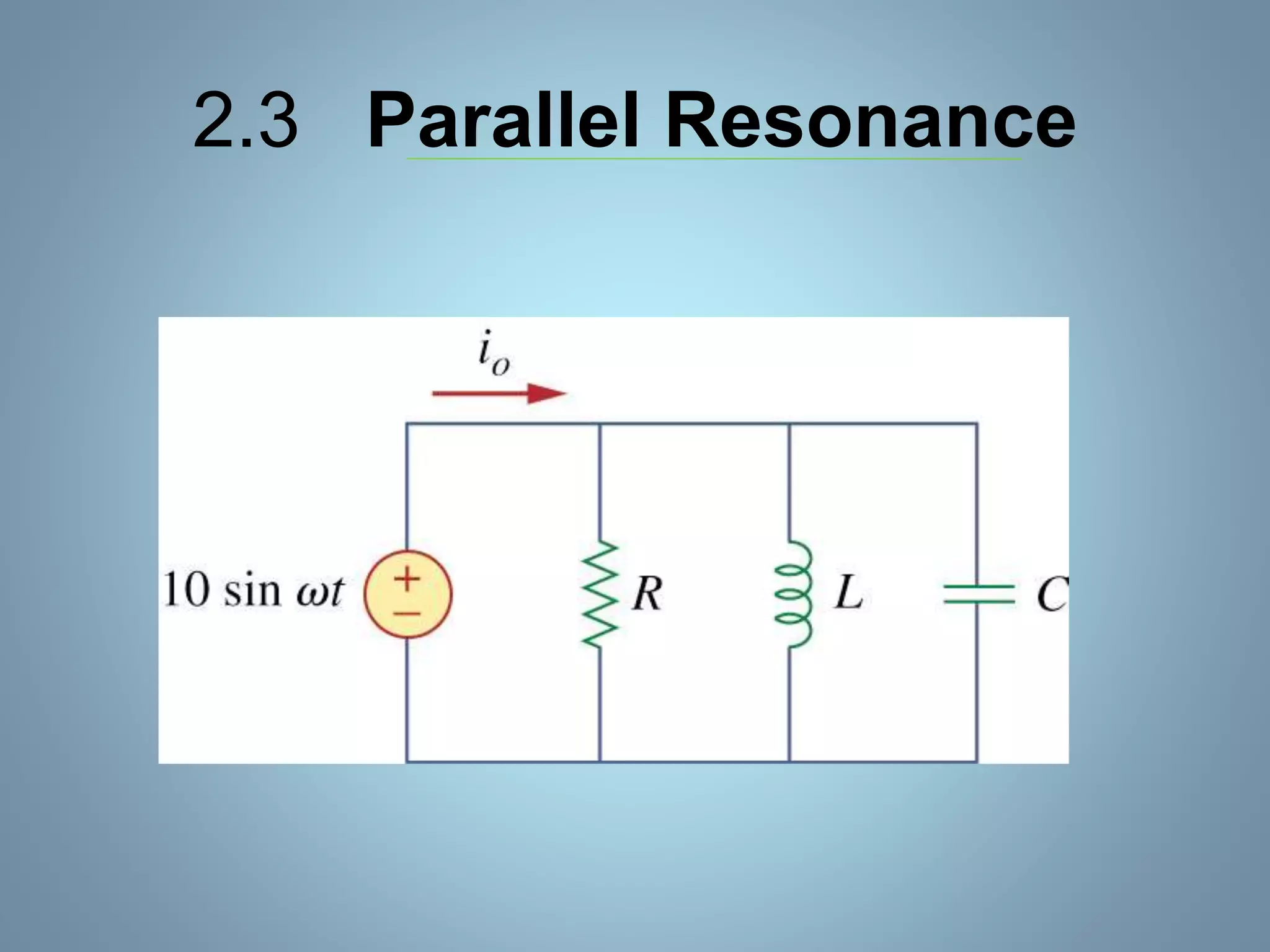
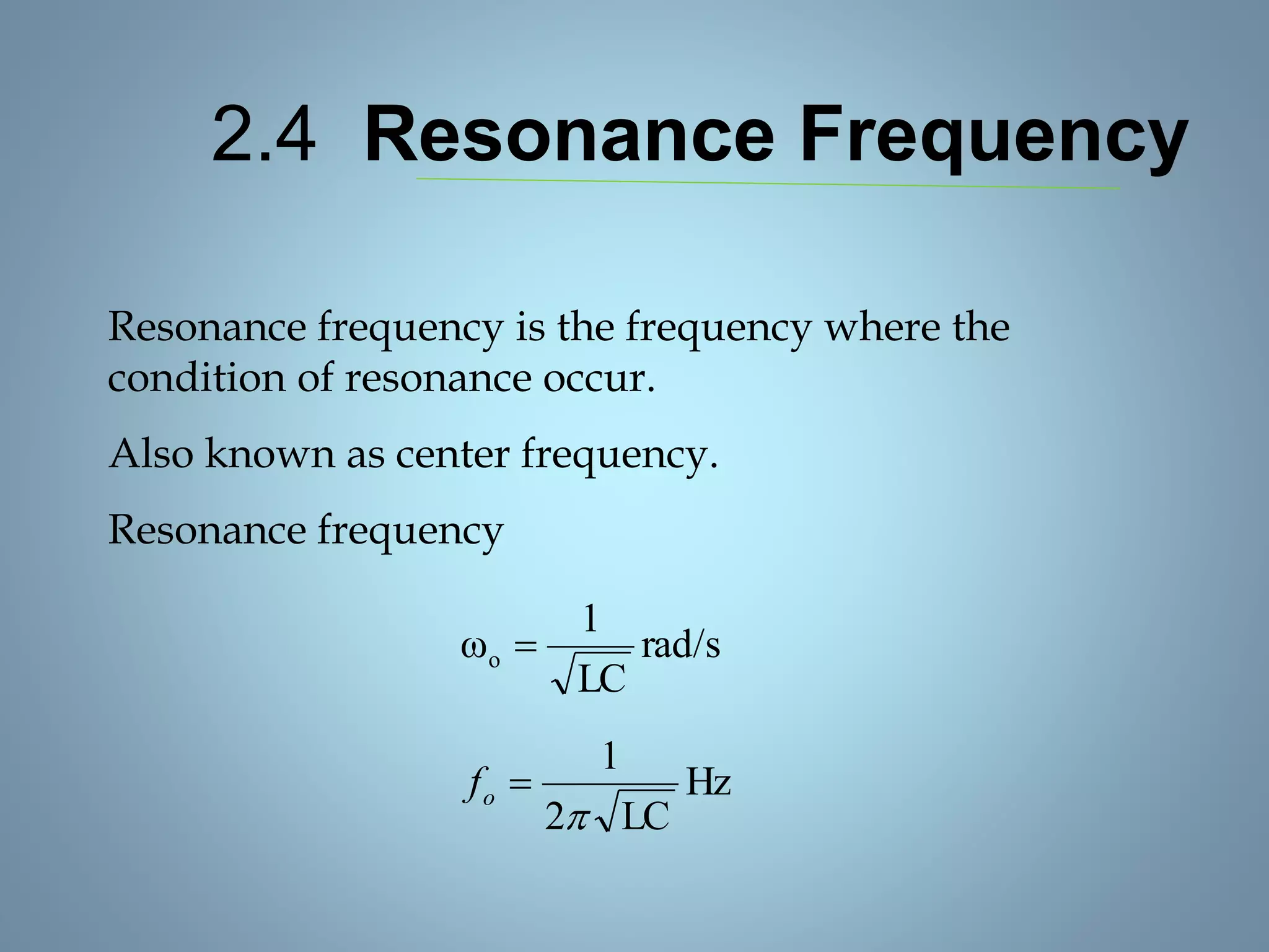
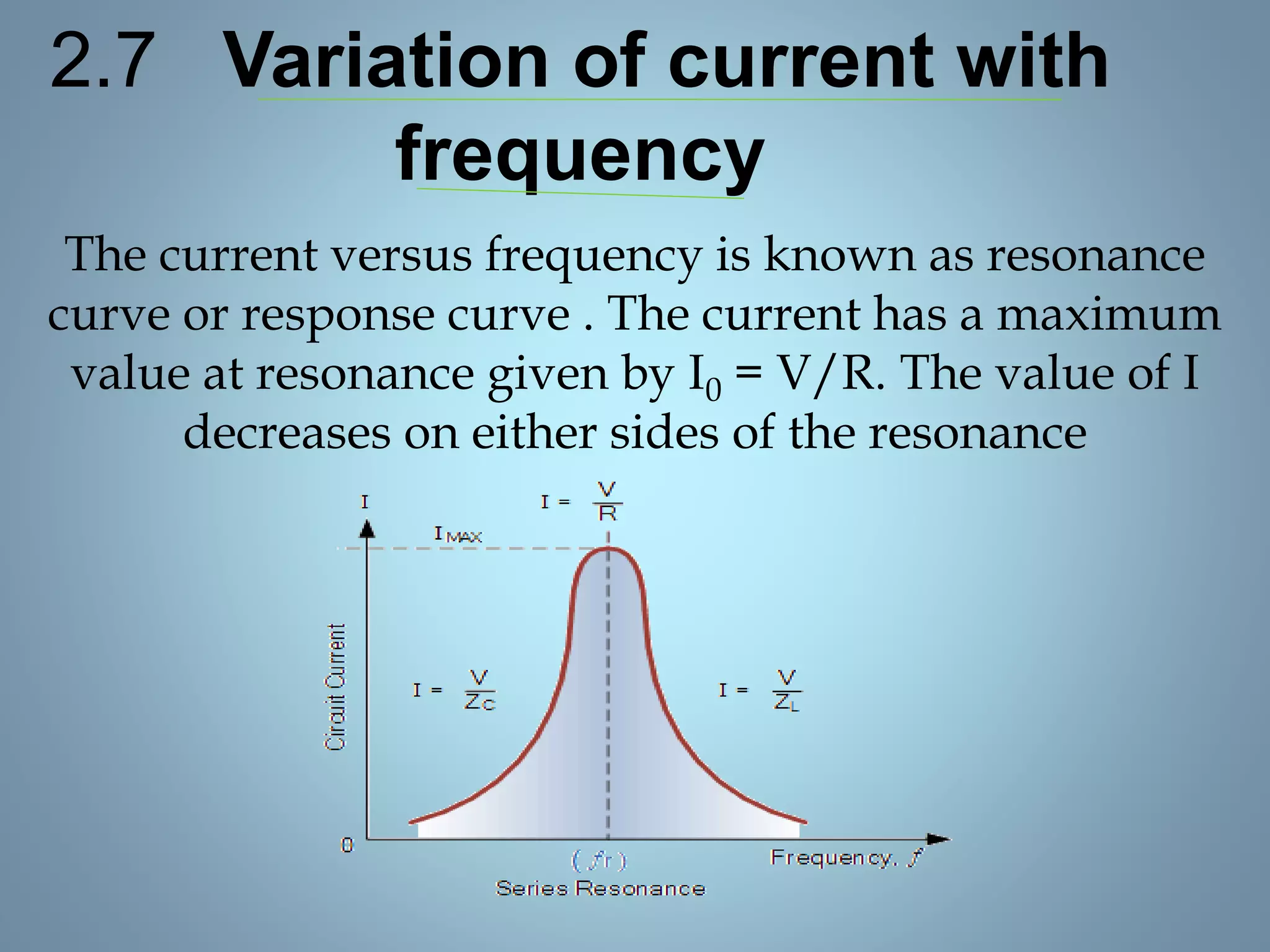
SEMINAR
ON
SINGLE PHASE AC
CIRCUITS ANALYSIS
Presented by:
Pranav Gupta
Roll No. 5
Section C
Branch: CIVIL
Graphic Era University, Dehradun
April, 2016
CONTENTS
1. AC CIRCUIT
1.1 PURELY RESISTIVE CICUIT
1.2 PURELY INDUCTIVE CIRCUIT
1.3 PURELY CAPACITIVE CIRCUIT
AC SERIES CIRCUITS
1.4 SERIES R-L CIRCUIT
1.5 SERIES R-C CIRCUIT
1.6 SERIES R-L-C CIRCUIT
CONTENTS
• 2. RESONANCE
• 2.1 RESONANCE IN SERIES
• 2.2 RESONANCE IN PARALLEL
• 2.3 RESONANCE FREQUENCY
VARIATION OF DIFF. QUANTITIES WITH
FREQUENCY
2.5 INDUCTIVE REACTANCE
2.6 CAPACITIVE REACTANCE
2.7 CURRENT
Introduction
AC CIRCUIT:
Circuits in which currents and voltages vary
sinusoidally i,e vary with time are called
alternating current or a.c circuits. All a.c circuits
are made up of combination of resistance R ,
inductance L and capacitance C. The circuit
elements R,L and C are called circuit parameters .
To study a general a.c circuit it is necessary to
consider the effect of each seperately.
1.1 Purely Resistive Circuits
• Figure shows a circuit containing only resistance R
• v = Vm sin ωt
• By Ohm’s law, the instantaneous current in the circuit will be
• i =v/R =Vm sinωt / R
• Vm
^/ R = Im
• i=Im sinωt
• Comparison of voltage equation and current shows that the phase difference
are in phase difference between voltage and current is zero . Hence , in a
circuit with resistance only the voltage and current are in phase with each
other .
The waveform and phase diagram respectively of
the voltage and current in a circuit containing only a
resistance .
Since maximum value = √2 * r.m.s. Value
Im = √2 I: Vm = √2 V
√2 V/R = √2 I
V = RI
Above eq=n represents ohm’s law
It is noted that applied voltage is counter balanced
by the voltage drop across the resistance R . This
voltage drop is called resistive voltage drop and
denoted by Vr .
Vr = V
Vr = IR
1.2 Purely Inductive Circuit
• Consider a purely inductive circuit containing only an inductance L
. Let the current taken by the circuit be
I = Imsinωt
This current produces a self induced e.m.f. eL
in the circuit given by
eL= -L di/dt
At any instant two voltages are present in the circuit , one is the
applied voltage eL . By KVL
v = - eL = L di/dt = L d(Imsin ωt)/dt
= ωLImcosωt = ωLImsin(ωt+ 900)
If ωLIm = Vm
v = Vm sin(ωt+ 900)
Comparison shows that the phase difference between voltage and
current is 90 .
• If Φ is measured from the current phase Φ =
+900 .
• Hence , in a purely inductive circuit the
voltage leads the current by 900 or the
current lags by 900.
• The waveform and phasor diagram
respectively of the voltage and current
containing only on inductance .
Inductive Reactance
ωL( I I) = V
ωL = V/I
The quantity ωL is the ratio of the r.m.s. voltage
to r.m.s. current in purely inductive circuit . It
is called the inductive reactance of the circuit
and is denoted by the symbol XL . Since it is the
ratio of voltage and current it is measured in
ohms .
The opposition of inductance to the flow of
alternating current is defined as the inductive
reatance XL .
XL = ωL
= 2 πfL
Also , V = XL I
The voltage drop across the inductance L
is called the inductive voltage drop . It is
denoted by VL .
VL = V
VL = XL I
1.3 Purely Capacitive circuit
• Consider a purely capacitive circuit containing only a
capacitor C connected to an a.c. Supply voltage given
by
• v= Vmsin ωt
• The current in the circuit at any instant is
• i =dq/dt
• i =d (Cv)/dt = C dv/dt = C d(Vm
sinωt)/dt
• = ωCVm cos ωt = ωCVm
sin(ωt+900)
• ωCVm
^ = Im
• i = Im sin(ωt+900)
Comparison shows that the phase difference Φ
between the voltage and the current is 900. if Φ
is measured from the voltage phasor Φ =
+900.Hence in purely capacitive circuit current
leads the voltage by 900.The waveforms and
phasor diagram respectively for a circuit
containing capacitance alone.
Capacitive
Reactance
• ωC( √2V)= √2I
• V/I=1/ωC
• The ratio of r.m.s. Voltage to r.m.s. Current in a purely
capacitive circuit is called the capacitive reactance. It is defined as
the opposition offered by a purely capacitive circuit to the flow of
sinusoidal current. The capacitive reactance is denoted by Xc and
is measured in ohms.
• Xc= 1/ωC= 1/2πfC
• V/I= X
• V= XcI
• The part of the supply which charges the capacitor is known as
the capacititve voltage drop.
• Vc= V
• Vc= XcI
1.4 Series R-L Circuit
• Consider a circuit containing a resistance R and an
inductance L in series
• Let V = supply voltage
• I = circuit current
• VR = voltage drop across R = RI
• VL = voltage drop across L = XLI= 2πfLI
• ΦL = phase angle between I and V
• Since I is common to both elements R and L,this is used as
reference phasor. The voltage VR is in phase with I and VL
leads by 900 . The voltage V is the phasor sum of VR and VL
that is the phasor diagram:
• The triangle having VR,VL and V as its sides is
called voltage triangle for a series R-L circuit:
• The phase angle ΦL between the supply voltage
V and the circuit current I is the angle between
the hypotenuse and the side VR .It is seen that
the current I is lagging behind the voltage V in
an R-L circuit.
• V2 = V2
R + V2
L
• = (RI)2 + (XL I)2
• V2/I2 = R2 + X2
L
• V/I = √(R2 + X2
L)
• ZL = √(R2 + X2
L)
• ZL is called the impedance of a series R-l circuit
• ZL = V/I
• V = ZL I
Impedance Triangle for a Series R-
L Circuit
• If the length of each side of the voltage triangle
is divided by current I , the impedance triangle
is obtained . The impedance triangle for a
series R-L circuit is given. The following
results may be found from an impedance
triangle for a series R-L circuit:
• ZL = √(R2 + X2
L)
• R = ZLcosΦL
• XL = ZL sinΦL
• tanΦL = XL /R
1.5 Series R-C
Circuit
• A circuit containing a resistance R and a
capacitance C in series
• Let V = supply voltage
• I = circuit current
• VR = voltage drop across R = RI
• VC = voltage drop across C =XCI =
I/2πfC
• ΦC = phase angle between I and V
• The voltage VR is in phase with I and VC lags
I by 900 .The voltage sum is:
• V = VR + VC
The phasor diagram:
The triangle having VR , Vc and V as its side is called voltage triangle for
a series R-C circuit.
The phase angle ΦC between the supply voltage and the circuit current
is the angle between the hypotenuse and the side VR . It is observed :
V2 = V2
R + V2
c
= (RI)2 + (Xc I)2
V2/I2 = R2 + X2
c
V/I = √(R2 + X2
c)
Zc = √(R2 + X2
c)
Zc is called the impedance of a series R-C circuit
Zc = V/I
V = Zc I
Impedance Triangle for a Series R-
C Circuit
If the length of each side of the voltage triangle
is divided by current I , the impedance triangle
is obtained . The impedance triangle for a
series R-C circuit is given. The following
results may be found from an impedance
triangle for a series R-C circuit:
ZC = √(R2 + X2
C)
R = ZCcosΦC
XC = ZC sinΦC
tanΦC = XC /R
1.6 Series RLC circuit
A circuit having R, l and C in series is called a general
series circuit current is used as reference phasor in
series circuit since it is common to all the elements of
circuit. There are four voltages
VR in phase with I
VL leading I by 900
VC lagging I by 900
Total voltage V = VR + VL + VC
Phasor diagram:
VL and VC are in opp. Directions and their
resultant is their arithmetic differnce
There are 3 possible cases in series RLC circuit
a. VL > VC i.e; Xl > XC
b. VL < VC i.e; Xl < XC
c. VL = VC i.e; Xl = XC
• When XL > XC the circuit is predominantly
inductive .
• # Inductive circuits cause the current ‘lag’ the
voltage.
• V=I √[R2 + ( Xl - XC )2]
• Z = √[R2 + ( Xl - XC )2]
• When XL < XC the circuit is predominately
capacitive.
• # Capacitive circuits cause the current to ‘lead’
the voltage.
• V=I √[R2 + ( Xc - Xl )2]
• Z = √[R2 + ( Xc - XL )2]
Impedance Triangle for RLC circuit
If the length of each side of a voltage triangle is
divided by current I, the impedance triangle is
obtained. The impedence triangle for series
RLC circuit :
2. RESONANCE
• Resonance is a condition in an RLC circuit in
which the capacitive and inductive reactance are
equal in magnitude, thereby resulting in a purely
resistive impedance.
• At resonance, the impedance consists only
resistive component R.
• The value of current will be maximum since the
total impedance is minimum.
• The voltage and current are in phase.
• Maximum power occurs at resonance since the
power factor is unity
• Resonance circuits are useful for constructing
filters and used in many application.
2.1 Series Resonance Circuit
2.2 Resonance in series RLC
circuit
CLTotal jX-jXRZ 
R
V
Z
V
I m
Total
s
m 
Total impedance of series RLC
Circuit is
At resonance
The impedance now
reduce to
CL XX 
RZTotal 
)X-j(XRZ CLTotal 
The current at resonance
2.3 Parallel Resonance
At resonance, currents IL and IC are equal and
cancelling giving a net reactive current equal to
zero. Then at resonance the above equation
becomes.
We remember that the total current flowing in a
parallel RLC circuit is equal to the vector sum of
the individual branch currents and for a given
frequency is calculated as:
2.4 Resonance Frequency
Resonance frequency is the frequency where the
condition of resonance occur.
Also known as center frequency.
Resonance frequency
rad/s
LC
1
ωo 
Hz
LC2
1

of
VARIATION OF DIFFERENT
QUANTITIES WITH FREQUENCY
2.5 Variation of inductive
reactance with frequency
The inductive reactance XL =2∏fL is directly
proportional to the frequency f .Hence its graph
is a straight line through the origin
2.6 Variation of capacitive
reactance with frequency
The capacitive reactance XC =1/2πfC is inversely
proportional to the frequency . Hence its graph is
a rectangular hyperbola XL versus f and XC
versus f curves cut at a point where f=f0
2.7 Variation of current with
frequency
The current versus frequency is known as resonance
curve or response curve . The current has a maximum
value at resonance given by I0 = V/R. The value of I
decreases on either sides of the resonance
THANK YOU

Single phase AC circuits

  • 1.
    SEMINAR ON SINGLE PHASE AC CIRCUITSANALYSIS Presented by: Pranav Gupta Roll No. 5 Section C Branch: CIVIL Graphic Era University, Dehradun April, 2016
  • 2.
    CONTENTS 1. AC CIRCUIT 1.1PURELY RESISTIVE CICUIT 1.2 PURELY INDUCTIVE CIRCUIT 1.3 PURELY CAPACITIVE CIRCUIT AC SERIES CIRCUITS 1.4 SERIES R-L CIRCUIT 1.5 SERIES R-C CIRCUIT 1.6 SERIES R-L-C CIRCUIT
  • 3.
    CONTENTS • 2. RESONANCE •2.1 RESONANCE IN SERIES • 2.2 RESONANCE IN PARALLEL • 2.3 RESONANCE FREQUENCY VARIATION OF DIFF. QUANTITIES WITH FREQUENCY 2.5 INDUCTIVE REACTANCE 2.6 CAPACITIVE REACTANCE 2.7 CURRENT
  • 4.
    Introduction AC CIRCUIT: Circuits inwhich currents and voltages vary sinusoidally i,e vary with time are called alternating current or a.c circuits. All a.c circuits are made up of combination of resistance R , inductance L and capacitance C. The circuit elements R,L and C are called circuit parameters . To study a general a.c circuit it is necessary to consider the effect of each seperately.
  • 5.
    1.1 Purely ResistiveCircuits • Figure shows a circuit containing only resistance R • v = Vm sin ωt • By Ohm’s law, the instantaneous current in the circuit will be • i =v/R =Vm sinωt / R • Vm ^/ R = Im • i=Im sinωt • Comparison of voltage equation and current shows that the phase difference are in phase difference between voltage and current is zero . Hence , in a circuit with resistance only the voltage and current are in phase with each other .
  • 6.
    The waveform andphase diagram respectively of the voltage and current in a circuit containing only a resistance . Since maximum value = √2 * r.m.s. Value Im = √2 I: Vm = √2 V √2 V/R = √2 I V = RI Above eq=n represents ohm’s law It is noted that applied voltage is counter balanced by the voltage drop across the resistance R . This voltage drop is called resistive voltage drop and denoted by Vr . Vr = V Vr = IR
  • 7.
    1.2 Purely InductiveCircuit • Consider a purely inductive circuit containing only an inductance L . Let the current taken by the circuit be I = Imsinωt This current produces a self induced e.m.f. eL in the circuit given by eL= -L di/dt At any instant two voltages are present in the circuit , one is the applied voltage eL . By KVL v = - eL = L di/dt = L d(Imsin ωt)/dt = ωLImcosωt = ωLImsin(ωt+ 900) If ωLIm = Vm v = Vm sin(ωt+ 900) Comparison shows that the phase difference between voltage and current is 90 .
  • 8.
    • If Φis measured from the current phase Φ = +900 . • Hence , in a purely inductive circuit the voltage leads the current by 900 or the current lags by 900. • The waveform and phasor diagram respectively of the voltage and current containing only on inductance .
  • 9.
    Inductive Reactance ωL( II) = V ωL = V/I The quantity ωL is the ratio of the r.m.s. voltage to r.m.s. current in purely inductive circuit . It is called the inductive reactance of the circuit and is denoted by the symbol XL . Since it is the ratio of voltage and current it is measured in ohms . The opposition of inductance to the flow of alternating current is defined as the inductive reatance XL .
  • 10.
    XL = ωL =2 πfL Also , V = XL I The voltage drop across the inductance L is called the inductive voltage drop . It is denoted by VL . VL = V VL = XL I
  • 11.
    1.3 Purely Capacitivecircuit • Consider a purely capacitive circuit containing only a capacitor C connected to an a.c. Supply voltage given by • v= Vmsin ωt • The current in the circuit at any instant is • i =dq/dt • i =d (Cv)/dt = C dv/dt = C d(Vm sinωt)/dt • = ωCVm cos ωt = ωCVm sin(ωt+900) • ωCVm ^ = Im • i = Im sin(ωt+900)
  • 12.
    Comparison shows thatthe phase difference Φ between the voltage and the current is 900. if Φ is measured from the voltage phasor Φ = +900.Hence in purely capacitive circuit current leads the voltage by 900.The waveforms and phasor diagram respectively for a circuit containing capacitance alone.
  • 13.
    Capacitive Reactance • ωC( √2V)=√2I • V/I=1/ωC • The ratio of r.m.s. Voltage to r.m.s. Current in a purely capacitive circuit is called the capacitive reactance. It is defined as the opposition offered by a purely capacitive circuit to the flow of sinusoidal current. The capacitive reactance is denoted by Xc and is measured in ohms. • Xc= 1/ωC= 1/2πfC • V/I= X • V= XcI • The part of the supply which charges the capacitor is known as the capacititve voltage drop. • Vc= V • Vc= XcI
  • 14.
    1.4 Series R-LCircuit • Consider a circuit containing a resistance R and an inductance L in series • Let V = supply voltage • I = circuit current • VR = voltage drop across R = RI • VL = voltage drop across L = XLI= 2πfLI • ΦL = phase angle between I and V • Since I is common to both elements R and L,this is used as reference phasor. The voltage VR is in phase with I and VL leads by 900 . The voltage V is the phasor sum of VR and VL that is the phasor diagram:
  • 15.
    • The trianglehaving VR,VL and V as its sides is called voltage triangle for a series R-L circuit: • The phase angle ΦL between the supply voltage V and the circuit current I is the angle between the hypotenuse and the side VR .It is seen that the current I is lagging behind the voltage V in an R-L circuit. • V2 = V2 R + V2 L • = (RI)2 + (XL I)2 • V2/I2 = R2 + X2 L • V/I = √(R2 + X2 L) • ZL = √(R2 + X2 L) • ZL is called the impedance of a series R-l circuit • ZL = V/I • V = ZL I
  • 16.
    Impedance Triangle fora Series R- L Circuit • If the length of each side of the voltage triangle is divided by current I , the impedance triangle is obtained . The impedance triangle for a series R-L circuit is given. The following results may be found from an impedance triangle for a series R-L circuit: • ZL = √(R2 + X2 L) • R = ZLcosΦL • XL = ZL sinΦL • tanΦL = XL /R
  • 17.
    1.5 Series R-C Circuit •A circuit containing a resistance R and a capacitance C in series • Let V = supply voltage • I = circuit current • VR = voltage drop across R = RI • VC = voltage drop across C =XCI = I/2πfC • ΦC = phase angle between I and V • The voltage VR is in phase with I and VC lags I by 900 .The voltage sum is: • V = VR + VC
  • 18.
    The phasor diagram: Thetriangle having VR , Vc and V as its side is called voltage triangle for a series R-C circuit. The phase angle ΦC between the supply voltage and the circuit current is the angle between the hypotenuse and the side VR . It is observed : V2 = V2 R + V2 c = (RI)2 + (Xc I)2 V2/I2 = R2 + X2 c V/I = √(R2 + X2 c) Zc = √(R2 + X2 c) Zc is called the impedance of a series R-C circuit Zc = V/I V = Zc I
  • 19.
    Impedance Triangle fora Series R- C Circuit If the length of each side of the voltage triangle is divided by current I , the impedance triangle is obtained . The impedance triangle for a series R-C circuit is given. The following results may be found from an impedance triangle for a series R-C circuit: ZC = √(R2 + X2 C) R = ZCcosΦC XC = ZC sinΦC tanΦC = XC /R
  • 20.
    1.6 Series RLCcircuit A circuit having R, l and C in series is called a general series circuit current is used as reference phasor in series circuit since it is common to all the elements of circuit. There are four voltages VR in phase with I VL leading I by 900 VC lagging I by 900 Total voltage V = VR + VL + VC
  • 21.
    Phasor diagram: VL andVC are in opp. Directions and their resultant is their arithmetic differnce There are 3 possible cases in series RLC circuit a. VL > VC i.e; Xl > XC b. VL < VC i.e; Xl < XC c. VL = VC i.e; Xl = XC
  • 22.
    • When XL> XC the circuit is predominantly inductive . • # Inductive circuits cause the current ‘lag’ the voltage. • V=I √[R2 + ( Xl - XC )2] • Z = √[R2 + ( Xl - XC )2] • When XL < XC the circuit is predominately capacitive. • # Capacitive circuits cause the current to ‘lead’ the voltage. • V=I √[R2 + ( Xc - Xl )2] • Z = √[R2 + ( Xc - XL )2]
  • 23.
    Impedance Triangle forRLC circuit If the length of each side of a voltage triangle is divided by current I, the impedance triangle is obtained. The impedence triangle for series RLC circuit :
  • 24.
    2. RESONANCE • Resonanceis a condition in an RLC circuit in which the capacitive and inductive reactance are equal in magnitude, thereby resulting in a purely resistive impedance. • At resonance, the impedance consists only resistive component R. • The value of current will be maximum since the total impedance is minimum. • The voltage and current are in phase. • Maximum power occurs at resonance since the power factor is unity • Resonance circuits are useful for constructing filters and used in many application.
  • 25.
  • 26.
    2.2 Resonance inseries RLC circuit CLTotal jX-jXRZ  R V Z V I m Total s m  Total impedance of series RLC Circuit is At resonance The impedance now reduce to CL XX  RZTotal  )X-j(XRZ CLTotal  The current at resonance
  • 27.
  • 28.
    At resonance, currentsIL and IC are equal and cancelling giving a net reactive current equal to zero. Then at resonance the above equation becomes.
  • 29.
    We remember thatthe total current flowing in a parallel RLC circuit is equal to the vector sum of the individual branch currents and for a given frequency is calculated as:
  • 30.
    2.4 Resonance Frequency Resonancefrequency is the frequency where the condition of resonance occur. Also known as center frequency. Resonance frequency rad/s LC 1 ωo  Hz LC2 1  of
  • 31.
  • 32.
    2.5 Variation ofinductive reactance with frequency The inductive reactance XL =2∏fL is directly proportional to the frequency f .Hence its graph is a straight line through the origin
  • 33.
    2.6 Variation ofcapacitive reactance with frequency The capacitive reactance XC =1/2πfC is inversely proportional to the frequency . Hence its graph is a rectangular hyperbola XL versus f and XC versus f curves cut at a point where f=f0
  • 34.
    2.7 Variation ofcurrent with frequency The current versus frequency is known as resonance curve or response curve . The current has a maximum value at resonance given by I0 = V/R. The value of I decreases on either sides of the resonance
  • 35.