Semiconductor improvement.pdf
•
0 likes•7 views

Wafer yield management plays a crucial role in semiconductor manufacturing by addressing various factors that can influence the efficiency and quality of the wafer manufacturing process.
Report
Share
Report
Share
Download to read offline
Recommended
Enhancing Quality Control with Statistical Process Control (SPC) in the Semic...
Enhancing Quality Control with Statistical Process Control (SPC) in the Semic...yieldWerx Semiconductor
Statistical Process Control Semiconductor (SPC) is a critical methodology in the realm of quality control, especially in the semiconductor manufacturing industry, that allows for a systematic approach to process improvement through the use of statistical analysis. The purpose of SPC is to get a comprehensive understanding of the variability in a process to enhance and ensure product quality, thereby positively impacting the overall performance of a manufacturing company.Harnessing the Power of Yield Management and Statistical Process Control in S...
Harnessing the Power of Yield Management and Statistical Process Control in S...yieldWerx Semiconductor
Semiconductor manufacturing sits at the nexus of technology, powering an array of devices that shape our modern world, from sophisticated Internet of Things (IoT) appliances to powerful computing systems. Navigating the high-demand landscape and ensuring an efficient production pipeline poses unique challenges due to the complex and intricate nature of semiconductor device fabrication. To meet these challenges, industry leaders employ advanced strategies such as yield management and statistical process control (SPC semiconductor). These key tools help maintain high yield rates, minimize defect densities, and optimize process parameters. In this in-depth exploration, we will shed light on the critical role of these statistical and analytical methodologies, examining their utilization for data-driven decision-making, process stability assessment, and system optimization in the semiconductor manufacturing arena.
The Indispensable Role of Outlier Detection for Ensuring Semiconductor Qualit...
The Indispensable Role of Outlier Detection for Ensuring Semiconductor Qualit...yieldWerx Semiconductor
Outlier Detection in the semiconductor industry plays a critical role in ensuring the quality and reliability of chips. By definition, outliers are results or objects that diverge significantly from standard values. Optimizing Semiconductor Yield with Robust WAT and PCM Processes.pptx
Wafer Acceptance Testing (WAT) and Process Control Monitoring (PCM) are instrumental elements within the semiconductor manufacturing industry. They are crucial tools utilized predominantly by fabless companies that seek to monitor and enhance their yield and defect rates.
The Significance of Enhanced Yield in Semiconductor Manufacturing.pptx
In the semiconductor manufacturing industry, the yield signifies the amount of product derived from a specific process. Yield can be evaluated in different dimensions such as die yield, wafer yield, and manufacturing yield. Enhancing yield is an intricate process involving rigorous data analysis and root cause identification to alleviate any bottlenecks in the manufacturing process.
Intricate Deep Dive into the Enhancement of Yield Management Strategies in Se...
Intricate Deep Dive into the Enhancement of Yield Management Strategies in Se...yieldWerx Semiconductor
Yield management is a key performance metric in the semiconductor industry. It is used to gauge the efficiency of a semiconductor manufacturing process by determining the percentage of wafers that are considered functional and are up to the mark based on predetermined standards. Unraveling the Secrets to Optimizing Yield in Semiconductor Manufacturing.pptx
Unraveling the Secrets to Optimizing Yield in Semiconductor Manufacturing.pptxyieldWerx Semiconductor
The semiconductor manufacturing industry is undergoing significant changes to address various challenges such as environmental sustainability, climate change, and the shift towards decentralized societies.Enhancing Semiconductor Manufacturing through Advanced Wafer Mapping.pptx
In the fast-paced semiconductor manufacturing industry, optimizing yield and maintaining high-quality standards are paramount. As integrated circuits continue to shrink in size and increase in complexity, the necessity for precise, advanced methodologies becomes ever more critical. Among the technologies employed, wafer map software stands out as an indispensable tool. Leveraging complex algorithms, color-coded grids, and innovative software functionalities, advanced wafer mapping enables real-time analysis of semiconductor wafers at an unparalleled level of detail. This technology has dramatically transformed the industry, providing insights into defect patterns, yield calculations, and testing processes, hence enhancing semiconductor manufacturing efficiency and productivity. This blog delves into the intricacies of wafer mapping, exploring its role, advancements, and impact on semiconductor manufacturing.
Amplifying the Power of Efficient Semiconductor Production with Next-Gen Wafe...
Amplifying the Power of Efficient Semiconductor Production with Next-Gen Wafe...yieldWerx Semiconductor
The semiconductor industry, with its rapid technological progression and intricate manufacturing processes, relies heavily on precision and control for optimum yield. In this sphere, an element that has become crucial to maintaining high-quality standards is advanced wafer mapping. By harnessing state-of-the-art algorithms, distinctive color-coded grids, and innovative software features, wafer mapping software furnishes a high-resolution analysis of semiconductor wafers in real time. This capability, in turn, boosts the efficacy and output of the semiconductor manufacturing industry. The ensuing discussion elucidates the fundamentals and advancements in wafer mapping, spotlighting its crucial role in semiconductor production.The Evolving Landscape of Semiconductor Manufacturing to Mitigate Yield Losse...
The Evolving Landscape of Semiconductor Manufacturing to Mitigate Yield Losse...yieldWerx Semiconductor
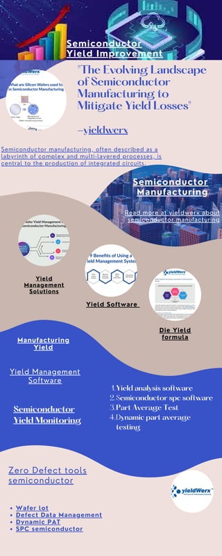
Semiconductor manufacturing, often described as a labyrinth of complex and multi-layered processes, is central to the production of integrated circuits. These circuits, already intricate, are becoming progressively more complex with each technological leap. This evolution intensifies the requirement for robust performance metrics, such as defect rate, semiconductor yield improvement, and cycle time. Through rigorous monitoring and analysis of these parameters, manufacturers can make significant enhancements to their performance, yielding a substantial impact on operational efficiency and profitability. This detailed exposition presents a comprehensive examination of yield modeling, dynamic capacity re-allocation mechanisms, yield competitiveness, and yield prediction models, offering invaluable insights for the semiconductor manufacturing industry.The Significance of Enhanced Yield in Semiconductor Manufacturing.pptx
In the semiconductor manufacturing industry, the yield signifies the amount of product derived from a specific process. Yield can be evaluated in different dimensions such as die yield, wafer yield, and manufacturing yield. Enhancing yield is an intricate process involving rigorous data analysis and root cause identification to alleviate any bottlenecks in the manufacturing process.
Addressing the Challenge of Wafer Map Classification in Semiconductor Manufac...
Addressing the Challenge of Wafer Map Classification in Semiconductor Manufac...yieldWerx Semiconductor
The field of semiconductor manufacturing is an intricate and intensive process that involves numerous complex chemical and physical operations. The final yield of the process, which signifies the percentage of functional chips produced from a silicon wafer, is a primary measure of a fabrication plant's efficiency. However, this yield is often affected by a multitude of factors, including equipment malfunctions, material impurities, and errors in process control.
Fault detection and classification play a crucial role in optimizing the yield of the process. These faults can be detected and classified by analyzing wafer maps, which are essentially two-dimensional representations of each die on a silicon wafer. The wafer map software display defect patterns that correspond to issues in manufacturing, with each defect having a unique signature that provides clues about the source of the problem.
Outlier Detection in Data Mining An Essential Component of Semiconductor Manu...
Outlier Detection in Data Mining An Essential Component of Semiconductor Manu...yieldWerx Semiconductor
Outlier detection is a critical research field within data mining due to its vast range of applications including fraud detection, cybersecurity, health diagnostics, and significantly for the semiconductor manufacturing industry. It refers to identifying data points that significantly deviate from expected patterns, providing crucial insights into different aspects of data. However, the ambiguity between outliers and normal behavior, evolving definitions of 'normal', application-specific techniques, and noisy data mimicking outliers, often complicate the outlier detection process. This review article offers an in-depth analysis of the most advanced outlier detection methods, presenting a thorough understanding of future research prospects.Innovating Quality Control in the Semiconductor Manufacturing Industry.pptx
The semiconductor manufacturing industry, a high-volume manufacturing environment characterized by its intricacy, stands as a testament to precision and performance. To ensure optimal outcomes, it is vital to maintain consistent quality control, with a special emphasis on the rectification of tool deterioration. Implementing innovative strategies related to process control monitoring can mitigate this problem and set a path towards a 'zero equipment failure' environment.
The Role and Detection of Outliers in Semiconductor Quality Control.pptx
In the intricately interconnected world of semiconductor manufacturing, the pursuit of quality control plays a pivotal role in ensuring the performance, reliability, and longevity of microelectronic devices. Central to this endeavor is the identification and management of outliers, anomalous data points that deviate significantly from the rest. These outliers, often indicative of underlying issues in the manufacturing process, can profoundly impact the functionality and integrity of the final product.
This document delves into the nature of outliers, the mechanisms to detect them, and their overarching role in the realm of semiconductor quality control. Through a deeper understanding of these elements, we aim to enhance the industry's ability to effectively manage and mitigate the risks associated with these statistical anomalies.
A Holistic Approach to Yield Improvement in the Semiconductor Manufacturing I...
A Holistic Approach to Yield Improvement in the Semiconductor Manufacturing I...yieldWerx Semiconductor
Semiconductor manufacturing is one of the most complex and competitive industries, heavily driven by innovation and cost-efficiency. It is continuously grappling with increasing cost pressures while concurrently working to meet the demands of rapidly advancing technology. Yield optimization, a multifaceted process aimed at improving the number of usable chips produced from raw materials, is an integral part of reducing manufacturing costs. This process involves taking into account several elements, such as equipment performance, operator capability, and the complexity of the design.Process Control Monitoring (PCM) and Wafer Acceptance Test (WAT) in the Semic...
Process Control Monitoring (PCM) and Wafer Acceptance Test (WAT) in the Semic...yieldWerx Semiconductor
Semiconductor manufacturing is an intricate process involving numerous stages, from wafer preparation to the final packaging of the integrated circuit. Two critical components of this process are Process Control Monitoring (PCM) and Wafer Acceptance Testing (WAT). PCM and WAT data are crucial in verifying the quality of the wafer at the end of fabrication, identifying potential defects, and ensuring the consistent production of high-quality semiconductor devices.Improving Yield and Quality in Semiconductor Manufacturing with Indispensable...
Improving Yield and Quality in Semiconductor Manufacturing with Indispensable...yieldWerx Semiconductor
Semiconductor manufacturing plays a vital role in the production of electronic devices, powering industries ranging from consumer electronics to automotive and aerospace. As technology advances, there is a growing demand for higher yields and improved reliability in the semiconductor manufacturing process. This blog will explore the challenges faced in semiconductor manufacturing, discuss the importance of yield and reliability, and highlight various strategies and technologies employed to enhance yield management and overall efficiency.Essentials of Gauge R&R in Ensuring Quality in Semiconductor Manufacturing.pptx
Essentials of Gauge R&R in Ensuring Quality in Semiconductor Manufacturing.pptxyieldWerx Semiconductor
The semiconductor industry is a cornerstone of modern technology, with applications ranging from consumer electronics to medical equipment. With the level of precision required in this sector, the demand for maintaining high-quality standards and minimizing variability is immense. One of the key statistical tools used in this pursuit of perfection is Gauge Repeatability and Reproducibility (Gauge R&R), which plays an indispensable role for improved yield in semiconductor manufacturing.
The criticality of Gauge R&R emerges from its ability to assess the deviations and variability caused by measurement systems, tools, or operators. It ensures that measurements taken by testing devices remain within specified tolerances, hence maintaining production consistency and mitigating potential losses due to faulty products.
Maximizing Production Efficiency with Big Data Analytics in semiconductor Man...
Maximizing Production Efficiency with Big Data Analytics in semiconductor Man...yieldWerx Semiconductor
Semiconductor manufacturing is a complex, high-tech process that generates a large volume of data. Utilizing this data effectively is critical for improving production yield, maintaining product quality, and driving efficiency across operations. Enter big-data analytics. While the term “big data” often refers to vast data sets that are too large for traditional data-processing tools to handle, its importance in the semiconductor manufacturing industry can't be understated. Big-data and yield analytics not only provides ways to process, analyze, and draw insights from these large volumes of data but also facilitates more efficient decision-making, informed by detailed, real-time data insights.Analytics Solutions for the Semiconductor Manufacturing Industry.pptx
The semiconductor industry faces several challenges that impact the effectiveness of yield analytics solutions. These challenges include equipment and process complexity, process dynamics, and data quality. To overcome these challenges, the industry recognizes the need for domain or subject matter expertise (SME) in tool process and analytics.
Analytics and yms solutions are crucial for addressing the challenges in the semiconductor data manufacturing industry. These yield management solutions leverage advanced techniques and subject matter expertise to overcome complexity, manage process dynamics, and improve data quality. By incorporating expertise, analytics solutions effectively analyze and control the semiconductor manufacturing process. Next-generation Fault Detection and Classification (NG-FDC) techniques offer improved accuracy and efficiency by incorporating automated analysis and SME knowledge. Overall, integrating subject matter expertise is essential for achieving robust manufacturing processes and enhanced performance in the semiconductor industry.
Advanced Methods for Outlier Detection and Analysis in Semiconductor Manufact...
Advanced Methods for Outlier Detection and Analysis in Semiconductor Manufact...yieldWerx Semiconductor
The semiconductor manufacturing industry faces numerous challenges due to its complex equipment and dynamic processes. To overcome these challenges and enhance operational efficiency, there is a growing emphasis on integrating domain expertise and utilizing advanced analytical solutions. This article explores the concept of outliers in semiconductor manufacturing, delves into outlier detection methods, highlights the significance of outlier analysis in semiconductor yield monitoring, and discusses the role of semiconductor data in driving effective analytics.Understanding the Dynamics of Semiconductor Manufacturing Yield Analysis and ...
Understanding the Dynamics of Semiconductor Manufacturing Yield Analysis and ...yieldWerx Semiconductor
The science and art of semiconductor manufacturing, responsible for powering the digital revolution, constitute one of the most intricate, detailed, and complicated processes of the modern industrial world. The essence of this complex multistage operation lies in creating integrated circuits, miniature electronic circuits that have found their way into almost every electronic device. These electronic marvels govern our digital world, from computers and smartphones to cars and kitchen appliances, and beyond.
The manufacturing of these semiconductors is a fascinating process that involves several layers of science - physics, chemistry, materials science - and combines them with precision engineering to create devices that are continuously shrinking in size while increasing in capabilities. This process is a testament to human ingenuity, involving billions of dollars of advanced equipment, and is growing increasingly complex due to reductions in feature size and the rising number of devices. However, amid this complexity, certain aspects stand out due to their impact on the manufacturing process: Semiconductor Yield Analysis, the Fabless Semiconductor business model, and Yield Management Systems.
Enhancing Yield in IC Design and Elevating YMS with AI and Machine Learning.pptx
Enhancing Yield in IC Design and Elevating YMS with AI and Machine Learning.pptxyieldWerx Semiconductor
In the rapidly evolving landscape of semiconductor manufacturing, two key areas stand at the forefront of driving efficiency and productivity - Yield in Integrated Circuit (IC) design and the use of artificial intelligence (AI) and machine learning in Yield Management Systems (YMS). Enhancing the yield of ICs during the design stage and incorporating advanced AI techniques in YMS can significantly transform the semiconductor manufacturing process, leading to improved operational efficiency, reduced costs, and high-quality products. This article delves into these critical areas, exploring how optimizing IC design can maximize yield and how AI and machine learning can augment YMS to unlock new levels of productivity and efficiency in semiconductor manufacturing.Technological Advancements in Semiconductor Manufacturing.pptx
Semiconductor manufacturing and semiconductor yield management is becoming more complex due to relentless advancements in technology. The ability to control critical dimensions is becoming increasingly important yet challenging as manufacturing processes continue to evolve. New production processes and variable machine configurations contribute to the complexity, generating high-dimensional, multi-collinear data that are difficult to analyze.
This intricate web of process data can be a hindrance in identifying the root causes of low yields or "excursions." However, data-driven methodologies present a powerful solution for these challenges. The implementation of big data analytics and machine learning techniques can help parse the overwhelming amount of data and extract insightful conclusions from it.
Semiconductors in Automotive Industry The Rise of Dynamic PAT and Advanced Ou...
Semiconductors in Automotive Industry The Rise of Dynamic PAT and Advanced Ou...yieldWerx Semiconductor
The automotive industry is undergoing significant transformations in the realm of semiconductor technologies utilized in vehicles. With the increasing number of chips in cars and the growing levels of automation, traditional part average testing (PAT) methods are no longer sufficient to ensure the desired levels of quality and reliability.
While PAT has been a prevalent practice in the automotive sector for nearly three decades, relying on statistical control limits to enhance yield and end-of-the-line quality, the emergence of advanced AI systems and autonomous driving technologies necessitates the adoption of more sophisticated outlier detection techniques and enhanced inspection and test coverage.
Zero Defects in Semiconductor Manufacturing for Automotive Applications.pptx
The semiconductor industry plays a critical role in providing electronic components for automotive applications. With the increasing complexity and reliance on electronic systems in vehicles, the need for zero defects in semiconductor manufacturing has become paramount. Automotive customers demand high-quality components to ensure the reliability, safety, and performance of their vehicles. Therefore, semiconductor manufacturers are focusing on implementing stringent quality control measures to minimize defects, reduce field returns and warranty issues, and mitigate liability concerns.
Machine Learning and Data Analytics in Semiconductor Yield Management.pptx
In the semiconductor manufacturing industry, the need for continuous quality improvement has never been more pronounced. This demand is driven by an unprecedented influx of manufacturing data, with more than 1000 process parameters recorded for a single wafer, and tens of thousands of wafers being produced daily. Traditional statistical methods have proven insufficient to fully exploit these massive volumes of data.
As such, this paper explores the application of hybrid machine learning techniques, specifically Memory Based Reasoning (MBR) and Neural Network (NN) learning, as more powerful tools for managing this complexity and improving yield in semiconductor manufacturing.
Bits & Pixels using AI for Good.........
A whirlwind tour of tech & AI for socio-environmental impact.
LF Energy Webinar: Electrical Grid Modelling and Simulation Through PowSyBl -...
Do you want to learn how to model and simulate an electrical network from scratch in under an hour?
Then welcome to this PowSyBl workshop, hosted by Rte, the French Transmission System Operator (TSO)!
During the webinar, you will discover the PowSyBl ecosystem as well as handle and study an electrical network through an interactive Python notebook.
PowSyBl is an open source project hosted by LF Energy, which offers a comprehensive set of features for electrical grid modelling and simulation. Among other advanced features, PowSyBl provides:
- A fully editable and extendable library for grid component modelling;
- Visualization tools to display your network;
- Grid simulation tools, such as power flows, security analyses (with or without remedial actions) and sensitivity analyses;
The framework is mostly written in Java, with a Python binding so that Python developers can access PowSyBl functionalities as well.
What you will learn during the webinar:
- For beginners: discover PowSyBl's functionalities through a quick general presentation and the notebook, without needing any expert coding skills;
- For advanced developers: master the skills to efficiently apply PowSyBl functionalities to your real-world scenarios.
More Related Content
More from yieldWerx Semiconductor
Amplifying the Power of Efficient Semiconductor Production with Next-Gen Wafe...
Amplifying the Power of Efficient Semiconductor Production with Next-Gen Wafe...yieldWerx Semiconductor
The semiconductor industry, with its rapid technological progression and intricate manufacturing processes, relies heavily on precision and control for optimum yield. In this sphere, an element that has become crucial to maintaining high-quality standards is advanced wafer mapping. By harnessing state-of-the-art algorithms, distinctive color-coded grids, and innovative software features, wafer mapping software furnishes a high-resolution analysis of semiconductor wafers in real time. This capability, in turn, boosts the efficacy and output of the semiconductor manufacturing industry. The ensuing discussion elucidates the fundamentals and advancements in wafer mapping, spotlighting its crucial role in semiconductor production.The Evolving Landscape of Semiconductor Manufacturing to Mitigate Yield Losse...
The Evolving Landscape of Semiconductor Manufacturing to Mitigate Yield Losse...yieldWerx Semiconductor
Semiconductor manufacturing, often described as a labyrinth of complex and multi-layered processes, is central to the production of integrated circuits. These circuits, already intricate, are becoming progressively more complex with each technological leap. This evolution intensifies the requirement for robust performance metrics, such as defect rate, semiconductor yield improvement, and cycle time. Through rigorous monitoring and analysis of these parameters, manufacturers can make significant enhancements to their performance, yielding a substantial impact on operational efficiency and profitability. This detailed exposition presents a comprehensive examination of yield modeling, dynamic capacity re-allocation mechanisms, yield competitiveness, and yield prediction models, offering invaluable insights for the semiconductor manufacturing industry.The Significance of Enhanced Yield in Semiconductor Manufacturing.pptx
In the semiconductor manufacturing industry, the yield signifies the amount of product derived from a specific process. Yield can be evaluated in different dimensions such as die yield, wafer yield, and manufacturing yield. Enhancing yield is an intricate process involving rigorous data analysis and root cause identification to alleviate any bottlenecks in the manufacturing process.
Addressing the Challenge of Wafer Map Classification in Semiconductor Manufac...
Addressing the Challenge of Wafer Map Classification in Semiconductor Manufac...yieldWerx Semiconductor
The field of semiconductor manufacturing is an intricate and intensive process that involves numerous complex chemical and physical operations. The final yield of the process, which signifies the percentage of functional chips produced from a silicon wafer, is a primary measure of a fabrication plant's efficiency. However, this yield is often affected by a multitude of factors, including equipment malfunctions, material impurities, and errors in process control.
Fault detection and classification play a crucial role in optimizing the yield of the process. These faults can be detected and classified by analyzing wafer maps, which are essentially two-dimensional representations of each die on a silicon wafer. The wafer map software display defect patterns that correspond to issues in manufacturing, with each defect having a unique signature that provides clues about the source of the problem.
Outlier Detection in Data Mining An Essential Component of Semiconductor Manu...
Outlier Detection in Data Mining An Essential Component of Semiconductor Manu...yieldWerx Semiconductor
Outlier detection is a critical research field within data mining due to its vast range of applications including fraud detection, cybersecurity, health diagnostics, and significantly for the semiconductor manufacturing industry. It refers to identifying data points that significantly deviate from expected patterns, providing crucial insights into different aspects of data. However, the ambiguity between outliers and normal behavior, evolving definitions of 'normal', application-specific techniques, and noisy data mimicking outliers, often complicate the outlier detection process. This review article offers an in-depth analysis of the most advanced outlier detection methods, presenting a thorough understanding of future research prospects.Innovating Quality Control in the Semiconductor Manufacturing Industry.pptx
The semiconductor manufacturing industry, a high-volume manufacturing environment characterized by its intricacy, stands as a testament to precision and performance. To ensure optimal outcomes, it is vital to maintain consistent quality control, with a special emphasis on the rectification of tool deterioration. Implementing innovative strategies related to process control monitoring can mitigate this problem and set a path towards a 'zero equipment failure' environment.
The Role and Detection of Outliers in Semiconductor Quality Control.pptx
In the intricately interconnected world of semiconductor manufacturing, the pursuit of quality control plays a pivotal role in ensuring the performance, reliability, and longevity of microelectronic devices. Central to this endeavor is the identification and management of outliers, anomalous data points that deviate significantly from the rest. These outliers, often indicative of underlying issues in the manufacturing process, can profoundly impact the functionality and integrity of the final product.
This document delves into the nature of outliers, the mechanisms to detect them, and their overarching role in the realm of semiconductor quality control. Through a deeper understanding of these elements, we aim to enhance the industry's ability to effectively manage and mitigate the risks associated with these statistical anomalies.
A Holistic Approach to Yield Improvement in the Semiconductor Manufacturing I...
A Holistic Approach to Yield Improvement in the Semiconductor Manufacturing I...yieldWerx Semiconductor
Semiconductor manufacturing is one of the most complex and competitive industries, heavily driven by innovation and cost-efficiency. It is continuously grappling with increasing cost pressures while concurrently working to meet the demands of rapidly advancing technology. Yield optimization, a multifaceted process aimed at improving the number of usable chips produced from raw materials, is an integral part of reducing manufacturing costs. This process involves taking into account several elements, such as equipment performance, operator capability, and the complexity of the design.Process Control Monitoring (PCM) and Wafer Acceptance Test (WAT) in the Semic...
Process Control Monitoring (PCM) and Wafer Acceptance Test (WAT) in the Semic...yieldWerx Semiconductor
Semiconductor manufacturing is an intricate process involving numerous stages, from wafer preparation to the final packaging of the integrated circuit. Two critical components of this process are Process Control Monitoring (PCM) and Wafer Acceptance Testing (WAT). PCM and WAT data are crucial in verifying the quality of the wafer at the end of fabrication, identifying potential defects, and ensuring the consistent production of high-quality semiconductor devices.Improving Yield and Quality in Semiconductor Manufacturing with Indispensable...
Improving Yield and Quality in Semiconductor Manufacturing with Indispensable...yieldWerx Semiconductor
Semiconductor manufacturing plays a vital role in the production of electronic devices, powering industries ranging from consumer electronics to automotive and aerospace. As technology advances, there is a growing demand for higher yields and improved reliability in the semiconductor manufacturing process. This blog will explore the challenges faced in semiconductor manufacturing, discuss the importance of yield and reliability, and highlight various strategies and technologies employed to enhance yield management and overall efficiency.Essentials of Gauge R&R in Ensuring Quality in Semiconductor Manufacturing.pptx
Essentials of Gauge R&R in Ensuring Quality in Semiconductor Manufacturing.pptxyieldWerx Semiconductor
The semiconductor industry is a cornerstone of modern technology, with applications ranging from consumer electronics to medical equipment. With the level of precision required in this sector, the demand for maintaining high-quality standards and minimizing variability is immense. One of the key statistical tools used in this pursuit of perfection is Gauge Repeatability and Reproducibility (Gauge R&R), which plays an indispensable role for improved yield in semiconductor manufacturing.
The criticality of Gauge R&R emerges from its ability to assess the deviations and variability caused by measurement systems, tools, or operators. It ensures that measurements taken by testing devices remain within specified tolerances, hence maintaining production consistency and mitigating potential losses due to faulty products.
Maximizing Production Efficiency with Big Data Analytics in semiconductor Man...
Maximizing Production Efficiency with Big Data Analytics in semiconductor Man...yieldWerx Semiconductor
Semiconductor manufacturing is a complex, high-tech process that generates a large volume of data. Utilizing this data effectively is critical for improving production yield, maintaining product quality, and driving efficiency across operations. Enter big-data analytics. While the term “big data” often refers to vast data sets that are too large for traditional data-processing tools to handle, its importance in the semiconductor manufacturing industry can't be understated. Big-data and yield analytics not only provides ways to process, analyze, and draw insights from these large volumes of data but also facilitates more efficient decision-making, informed by detailed, real-time data insights.Analytics Solutions for the Semiconductor Manufacturing Industry.pptx
The semiconductor industry faces several challenges that impact the effectiveness of yield analytics solutions. These challenges include equipment and process complexity, process dynamics, and data quality. To overcome these challenges, the industry recognizes the need for domain or subject matter expertise (SME) in tool process and analytics.
Analytics and yms solutions are crucial for addressing the challenges in the semiconductor data manufacturing industry. These yield management solutions leverage advanced techniques and subject matter expertise to overcome complexity, manage process dynamics, and improve data quality. By incorporating expertise, analytics solutions effectively analyze and control the semiconductor manufacturing process. Next-generation Fault Detection and Classification (NG-FDC) techniques offer improved accuracy and efficiency by incorporating automated analysis and SME knowledge. Overall, integrating subject matter expertise is essential for achieving robust manufacturing processes and enhanced performance in the semiconductor industry.
Advanced Methods for Outlier Detection and Analysis in Semiconductor Manufact...
Advanced Methods for Outlier Detection and Analysis in Semiconductor Manufact...yieldWerx Semiconductor
The semiconductor manufacturing industry faces numerous challenges due to its complex equipment and dynamic processes. To overcome these challenges and enhance operational efficiency, there is a growing emphasis on integrating domain expertise and utilizing advanced analytical solutions. This article explores the concept of outliers in semiconductor manufacturing, delves into outlier detection methods, highlights the significance of outlier analysis in semiconductor yield monitoring, and discusses the role of semiconductor data in driving effective analytics.Understanding the Dynamics of Semiconductor Manufacturing Yield Analysis and ...
Understanding the Dynamics of Semiconductor Manufacturing Yield Analysis and ...yieldWerx Semiconductor
The science and art of semiconductor manufacturing, responsible for powering the digital revolution, constitute one of the most intricate, detailed, and complicated processes of the modern industrial world. The essence of this complex multistage operation lies in creating integrated circuits, miniature electronic circuits that have found their way into almost every electronic device. These electronic marvels govern our digital world, from computers and smartphones to cars and kitchen appliances, and beyond.
The manufacturing of these semiconductors is a fascinating process that involves several layers of science - physics, chemistry, materials science - and combines them with precision engineering to create devices that are continuously shrinking in size while increasing in capabilities. This process is a testament to human ingenuity, involving billions of dollars of advanced equipment, and is growing increasingly complex due to reductions in feature size and the rising number of devices. However, amid this complexity, certain aspects stand out due to their impact on the manufacturing process: Semiconductor Yield Analysis, the Fabless Semiconductor business model, and Yield Management Systems.
Enhancing Yield in IC Design and Elevating YMS with AI and Machine Learning.pptx
Enhancing Yield in IC Design and Elevating YMS with AI and Machine Learning.pptxyieldWerx Semiconductor
In the rapidly evolving landscape of semiconductor manufacturing, two key areas stand at the forefront of driving efficiency and productivity - Yield in Integrated Circuit (IC) design and the use of artificial intelligence (AI) and machine learning in Yield Management Systems (YMS). Enhancing the yield of ICs during the design stage and incorporating advanced AI techniques in YMS can significantly transform the semiconductor manufacturing process, leading to improved operational efficiency, reduced costs, and high-quality products. This article delves into these critical areas, exploring how optimizing IC design can maximize yield and how AI and machine learning can augment YMS to unlock new levels of productivity and efficiency in semiconductor manufacturing.Technological Advancements in Semiconductor Manufacturing.pptx
Semiconductor manufacturing and semiconductor yield management is becoming more complex due to relentless advancements in technology. The ability to control critical dimensions is becoming increasingly important yet challenging as manufacturing processes continue to evolve. New production processes and variable machine configurations contribute to the complexity, generating high-dimensional, multi-collinear data that are difficult to analyze.
This intricate web of process data can be a hindrance in identifying the root causes of low yields or "excursions." However, data-driven methodologies present a powerful solution for these challenges. The implementation of big data analytics and machine learning techniques can help parse the overwhelming amount of data and extract insightful conclusions from it.
Semiconductors in Automotive Industry The Rise of Dynamic PAT and Advanced Ou...
Semiconductors in Automotive Industry The Rise of Dynamic PAT and Advanced Ou...yieldWerx Semiconductor
The automotive industry is undergoing significant transformations in the realm of semiconductor technologies utilized in vehicles. With the increasing number of chips in cars and the growing levels of automation, traditional part average testing (PAT) methods are no longer sufficient to ensure the desired levels of quality and reliability.
While PAT has been a prevalent practice in the automotive sector for nearly three decades, relying on statistical control limits to enhance yield and end-of-the-line quality, the emergence of advanced AI systems and autonomous driving technologies necessitates the adoption of more sophisticated outlier detection techniques and enhanced inspection and test coverage.
Zero Defects in Semiconductor Manufacturing for Automotive Applications.pptx
The semiconductor industry plays a critical role in providing electronic components for automotive applications. With the increasing complexity and reliance on electronic systems in vehicles, the need for zero defects in semiconductor manufacturing has become paramount. Automotive customers demand high-quality components to ensure the reliability, safety, and performance of their vehicles. Therefore, semiconductor manufacturers are focusing on implementing stringent quality control measures to minimize defects, reduce field returns and warranty issues, and mitigate liability concerns.
Machine Learning and Data Analytics in Semiconductor Yield Management.pptx
In the semiconductor manufacturing industry, the need for continuous quality improvement has never been more pronounced. This demand is driven by an unprecedented influx of manufacturing data, with more than 1000 process parameters recorded for a single wafer, and tens of thousands of wafers being produced daily. Traditional statistical methods have proven insufficient to fully exploit these massive volumes of data.
As such, this paper explores the application of hybrid machine learning techniques, specifically Memory Based Reasoning (MBR) and Neural Network (NN) learning, as more powerful tools for managing this complexity and improving yield in semiconductor manufacturing.
More from yieldWerx Semiconductor (20)
Amplifying the Power of Efficient Semiconductor Production with Next-Gen Wafe...
Amplifying the Power of Efficient Semiconductor Production with Next-Gen Wafe...
The Evolving Landscape of Semiconductor Manufacturing to Mitigate Yield Losse...
The Evolving Landscape of Semiconductor Manufacturing to Mitigate Yield Losse...
The Significance of Enhanced Yield in Semiconductor Manufacturing.pptx
The Significance of Enhanced Yield in Semiconductor Manufacturing.pptx
Addressing the Challenge of Wafer Map Classification in Semiconductor Manufac...
Addressing the Challenge of Wafer Map Classification in Semiconductor Manufac...
Outlier Detection in Data Mining An Essential Component of Semiconductor Manu...
Outlier Detection in Data Mining An Essential Component of Semiconductor Manu...
Innovating Quality Control in the Semiconductor Manufacturing Industry.pptx
Innovating Quality Control in the Semiconductor Manufacturing Industry.pptx
The Role and Detection of Outliers in Semiconductor Quality Control.pptx
The Role and Detection of Outliers in Semiconductor Quality Control.pptx
A Holistic Approach to Yield Improvement in the Semiconductor Manufacturing I...
A Holistic Approach to Yield Improvement in the Semiconductor Manufacturing I...
Process Control Monitoring (PCM) and Wafer Acceptance Test (WAT) in the Semic...
Process Control Monitoring (PCM) and Wafer Acceptance Test (WAT) in the Semic...
Improving Yield and Quality in Semiconductor Manufacturing with Indispensable...
Improving Yield and Quality in Semiconductor Manufacturing with Indispensable...
Essentials of Gauge R&R in Ensuring Quality in Semiconductor Manufacturing.pptx
Essentials of Gauge R&R in Ensuring Quality in Semiconductor Manufacturing.pptx
Maximizing Production Efficiency with Big Data Analytics in semiconductor Man...
Maximizing Production Efficiency with Big Data Analytics in semiconductor Man...
Analytics Solutions for the Semiconductor Manufacturing Industry.pptx
Analytics Solutions for the Semiconductor Manufacturing Industry.pptx
Advanced Methods for Outlier Detection and Analysis in Semiconductor Manufact...
Advanced Methods for Outlier Detection and Analysis in Semiconductor Manufact...
Understanding the Dynamics of Semiconductor Manufacturing Yield Analysis and ...
Understanding the Dynamics of Semiconductor Manufacturing Yield Analysis and ...
Enhancing Yield in IC Design and Elevating YMS with AI and Machine Learning.pptx
Enhancing Yield in IC Design and Elevating YMS with AI and Machine Learning.pptx
Technological Advancements in Semiconductor Manufacturing.pptx
Technological Advancements in Semiconductor Manufacturing.pptx
Semiconductors in Automotive Industry The Rise of Dynamic PAT and Advanced Ou...
Semiconductors in Automotive Industry The Rise of Dynamic PAT and Advanced Ou...
Zero Defects in Semiconductor Manufacturing for Automotive Applications.pptx
Zero Defects in Semiconductor Manufacturing for Automotive Applications.pptx
Machine Learning and Data Analytics in Semiconductor Yield Management.pptx
Machine Learning and Data Analytics in Semiconductor Yield Management.pptx
Recently uploaded
Bits & Pixels using AI for Good.........
A whirlwind tour of tech & AI for socio-environmental impact.
LF Energy Webinar: Electrical Grid Modelling and Simulation Through PowSyBl -...
Do you want to learn how to model and simulate an electrical network from scratch in under an hour?
Then welcome to this PowSyBl workshop, hosted by Rte, the French Transmission System Operator (TSO)!
During the webinar, you will discover the PowSyBl ecosystem as well as handle and study an electrical network through an interactive Python notebook.
PowSyBl is an open source project hosted by LF Energy, which offers a comprehensive set of features for electrical grid modelling and simulation. Among other advanced features, PowSyBl provides:
- A fully editable and extendable library for grid component modelling;
- Visualization tools to display your network;
- Grid simulation tools, such as power flows, security analyses (with or without remedial actions) and sensitivity analyses;
The framework is mostly written in Java, with a Python binding so that Python developers can access PowSyBl functionalities as well.
What you will learn during the webinar:
- For beginners: discover PowSyBl's functionalities through a quick general presentation and the notebook, without needing any expert coding skills;
- For advanced developers: master the skills to efficiently apply PowSyBl functionalities to your real-world scenarios.
Slack (or Teams) Automation for Bonterra Impact Management (fka Social Soluti...
Sidekick Solutions uses Bonterra Impact Management (fka Social Solutions Apricot) and automation solutions to integrate data for business workflows.
We believe integration and automation are essential to user experience and the promise of efficient work through technology. Automation is the critical ingredient to realizing that full vision. We develop integration products and services for Bonterra Case Management software to support the deployment of automations for a variety of use cases.
This video focuses on the notifications, alerts, and approval requests using Slack for Bonterra Impact Management. The solutions covered in this webinar can also be deployed for Microsoft Teams.
Interested in deploying notification automations for Bonterra Impact Management? Contact us at sales@sidekicksolutionsllc.com to discuss next steps.
Transcript: Selling digital books in 2024: Insights from industry leaders - T...
The publishing industry has been selling digital audiobooks and ebooks for over a decade and has found its groove. What’s changed? What has stayed the same? Where do we go from here? Join a group of leading sales peers from across the industry for a conversation about the lessons learned since the popularization of digital books, best practices, digital book supply chain management, and more.
Link to video recording: https://bnctechforum.ca/sessions/selling-digital-books-in-2024-insights-from-industry-leaders/
Presented by BookNet Canada on May 28, 2024, with support from the Department of Canadian Heritage.
UiPath Test Automation using UiPath Test Suite series, part 3
Welcome to UiPath Test Automation using UiPath Test Suite series part 3. In this session, we will cover desktop automation along with UI automation.
Topics covered:
UI automation Introduction,
UI automation Sample
Desktop automation flow
Pradeep Chinnala, Senior Consultant Automation Developer @WonderBotz and UiPath MVP
Deepak Rai, Automation Practice Lead, Boundaryless Group and UiPath MVP
AI for Every Business: Unlocking Your Product's Universal Potential by VP of ...
AI for Every Business: Unlocking Your Product's Universal Potential by VP of Product, Slack
Leading Change strategies and insights for effective change management pdf 1.pdf
Leading Change strategies and insights for effective change management pdf 1.pdf
To Graph or Not to Graph Knowledge Graph Architectures and LLMs
Reflecting on new architectures for knowledge based systems in light of generative ai
GenAISummit 2024 May 28 Sri Ambati Keynote: AGI Belongs to The Community in O...
“AGI should be open source and in the public domain at the service of humanity and the planet.”
State of ICS and IoT Cyber Threat Landscape Report 2024 preview
The IoT and OT threat landscape report has been prepared by the Threat Research Team at Sectrio using data from Sectrio, cyber threat intelligence farming facilities spread across over 85 cities around the world. In addition, Sectrio also runs AI-based advanced threat and payload engagement facilities that serve as sinks to attract and engage sophisticated threat actors, and newer malware including new variants and latent threats that are at an earlier stage of development.
The latest edition of the OT/ICS and IoT security Threat Landscape Report 2024 also covers:
State of global ICS asset and network exposure
Sectoral targets and attacks as well as the cost of ransom
Global APT activity, AI usage, actor and tactic profiles, and implications
Rise in volumes of AI-powered cyberattacks
Major cyber events in 2024
Malware and malicious payload trends
Cyberattack types and targets
Vulnerability exploit attempts on CVEs
Attacks on counties – USA
Expansion of bot farms – how, where, and why
In-depth analysis of the cyber threat landscape across North America, South America, Europe, APAC, and the Middle East
Why are attacks on smart factories rising?
Cyber risk predictions
Axis of attacks – Europe
Systemic attacks in the Middle East
Download the full report from here:
https://sectrio.com/resources/ot-threat-landscape-reports/sectrio-releases-ot-ics-and-iot-security-threat-landscape-report-2024/
Generating a custom Ruby SDK for your web service or Rails API using Smithy
Have you ever wanted a Ruby client API to communicate with your web service? Smithy is a protocol-agnostic language for defining services and SDKs. Smithy Ruby is an implementation of Smithy that generates a Ruby SDK using a Smithy model. In this talk, we will explore Smithy and Smithy Ruby to learn how to generate custom feature-rich SDKs that can communicate with any web service, such as a Rails JSON API.
GraphRAG is All You need? LLM & Knowledge Graph
Guy Korland, CEO and Co-founder of FalkorDB, will review two articles on the integration of language models with knowledge graphs.
1. Unifying Large Language Models and Knowledge Graphs: A Roadmap.
https://arxiv.org/abs/2306.08302
2. Microsoft Research's GraphRAG paper and a review paper on various uses of knowledge graphs:
https://www.microsoft.com/en-us/research/blog/graphrag-unlocking-llm-discovery-on-narrative-private-data/
Connector Corner: Automate dynamic content and events by pushing a button
Here is something new! In our next Connector Corner webinar, we will demonstrate how you can use a single workflow to:
Create a campaign using Mailchimp with merge tags/fields
Send an interactive Slack channel message (using buttons)
Have the message received by managers and peers along with a test email for review
But there’s more:
In a second workflow supporting the same use case, you’ll see:
Your campaign sent to target colleagues for approval
If the “Approve” button is clicked, a Jira/Zendesk ticket is created for the marketing design team
But—if the “Reject” button is pushed, colleagues will be alerted via Slack message
Join us to learn more about this new, human-in-the-loop capability, brought to you by Integration Service connectors.
And...
Speakers:
Akshay Agnihotri, Product Manager
Charlie Greenberg, Host
Knowledge engineering: from people to machines and back
Keynote at the 21st European Semantic Web Conference
From Siloed Products to Connected Ecosystem: Building a Sustainable and Scala...
From Siloed Products to Connected Ecosystem: Building a Sustainable and Scalable Platform by VP of Product, The New York Times
Accelerate your Kubernetes clusters with Varnish Caching
A presentation about the usage and availability of Varnish on Kubernetes. This talk explores the capabilities of Varnish caching and shows how to use the Varnish Helm chart to deploy it to Kubernetes.
This presentation was delivered at K8SUG Singapore. See https://feryn.eu/presentations/accelerate-your-kubernetes-clusters-with-varnish-caching-k8sug-singapore-28-2024 for more details.
Recently uploaded (20)
LF Energy Webinar: Electrical Grid Modelling and Simulation Through PowSyBl -...
LF Energy Webinar: Electrical Grid Modelling and Simulation Through PowSyBl -...
FIDO Alliance Osaka Seminar: Passkeys and the Road Ahead.pdf
FIDO Alliance Osaka Seminar: Passkeys and the Road Ahead.pdf
Slack (or Teams) Automation for Bonterra Impact Management (fka Social Soluti...
Slack (or Teams) Automation for Bonterra Impact Management (fka Social Soluti...
Transcript: Selling digital books in 2024: Insights from industry leaders - T...
Transcript: Selling digital books in 2024: Insights from industry leaders - T...
UiPath Test Automation using UiPath Test Suite series, part 3
UiPath Test Automation using UiPath Test Suite series, part 3
Monitoring Java Application Security with JDK Tools and JFR Events
Monitoring Java Application Security with JDK Tools and JFR Events
AI for Every Business: Unlocking Your Product's Universal Potential by VP of ...
AI for Every Business: Unlocking Your Product's Universal Potential by VP of ...
Leading Change strategies and insights for effective change management pdf 1.pdf
Leading Change strategies and insights for effective change management pdf 1.pdf
To Graph or Not to Graph Knowledge Graph Architectures and LLMs
To Graph or Not to Graph Knowledge Graph Architectures and LLMs
GenAISummit 2024 May 28 Sri Ambati Keynote: AGI Belongs to The Community in O...
GenAISummit 2024 May 28 Sri Ambati Keynote: AGI Belongs to The Community in O...
State of ICS and IoT Cyber Threat Landscape Report 2024 preview
State of ICS and IoT Cyber Threat Landscape Report 2024 preview
Generating a custom Ruby SDK for your web service or Rails API using Smithy
Generating a custom Ruby SDK for your web service or Rails API using Smithy
Connector Corner: Automate dynamic content and events by pushing a button
Connector Corner: Automate dynamic content and events by pushing a button
FIDO Alliance Osaka Seminar: Passkeys at Amazon.pdf
FIDO Alliance Osaka Seminar: Passkeys at Amazon.pdf
Knowledge engineering: from people to machines and back
Knowledge engineering: from people to machines and back
From Siloed Products to Connected Ecosystem: Building a Sustainable and Scala...
From Siloed Products to Connected Ecosystem: Building a Sustainable and Scala...
Accelerate your Kubernetes clusters with Varnish Caching
Accelerate your Kubernetes clusters with Varnish Caching
Semiconductor improvement.pdf
- 1. Yield Management Solutions Die Yield formula Yield Software "The Evolving Landscape of Semiconductor Manufacturing to Mitigate Yield Losses" -yieldwerx Semiconductor Yield Improvement Semiconductor manufacturing, often described as a labyrinth of complex and multi-layered processes, is central to the production of integrated circuits. Wafer lot Defect Data Management Dynamic PAT SPC semiconductor Semiconductor Yield Monitoring Yield analysis software Semiconductor spc software Part Average Test Dynamic part average testing 1. 2. 3. 4. Semiconductor Manufacturing Zero Defect tools semiconductor Read more at yieldwerx about semiconductor manufacturing Manufacturing Yield Yield Management Software