Semiconductor manufacturing is an intricate process involving numerous stages, from wafer preparation to the final packaging of the integrated circuit. Two critical components of this process are Process Control Monitoring (PCM) and Wafer Acceptance Testing (WAT). PCM and WAT data are crucial in verifying the quality of the wafer at the end of fabrication, identifying potential defects, and ensuring the consistent production of high-quality semiconductor devices.
Optimizing Semiconductor Yield with Robust WAT and PCM Processes.pptxyieldWerx Semiconductor
Wafer Acceptance Testing (WAT) and Process Control Monitoring (PCM) are instrumental elements within the semiconductor manufacturing industry. They are crucial tools utilized predominantly by fabless companies that seek to monitor and enhance their yield and defect rates.
Innovating Quality Control in the Semiconductor Manufacturing Industry.pptxyieldWerx Semiconductor
The semiconductor manufacturing industry, a high-volume manufacturing environment characterized by its intricacy, stands as a testament to precision and performance. To ensure optimal outcomes, it is vital to maintain consistent quality control, with a special emphasis on the rectification of tool deterioration. Implementing innovative strategies related to process control monitoring can mitigate this problem and set a path towards a 'zero equipment failure' environment.
In the fast-paced world of semiconductor manufacturing, preventing process excursions is crucial for optimizing yield, reducing wafer scraps, and efficiently allocating engineering and manufacturing resources.
Zero Defects in Semiconductor Manufacturing for Automotive Applications.pptxyieldWerx Semiconductor
The semiconductor industry plays a critical role in providing electronic components for automotive applications. With the increasing complexity and reliance on electronic systems in vehicles, the need for zero defects in semiconductor manufacturing has become paramount. Automotive customers demand high-quality components to ensure the reliability, safety, and performance of their vehicles. Therefore, semiconductor manufacturers are focusing on implementing stringent quality control measures to minimize defects, reduce field returns and warranty issues, and mitigate liability concerns.
Advanced Methods for Outlier Detection and Analysis in Semiconductor Manufact...yieldWerx Semiconductor
The semiconductor manufacturing industry faces numerous challenges due to its complex equipment and dynamic processes. To overcome these challenges and enhance operational efficiency, there is a growing emphasis on integrating domain expertise and utilizing advanced analytical solutions. This article explores the concept of outliers in semiconductor manufacturing, delves into outlier detection methods, highlights the significance of outlier analysis in semiconductor yield monitoring, and discusses the role of semiconductor data in driving effective analytics.
Enhancing Quality Control with Statistical Process Control (SPC) in the Semic...yieldWerx Semiconductor
Statistical Process Control Semiconductor (SPC) is a critical methodology in the realm of quality control, especially in the semiconductor manufacturing industry, that allows for a systematic approach to process improvement through the use of statistical analysis. The purpose of SPC is to get a comprehensive understanding of the variability in a process to enhance and ensure product quality, thereby positively impacting the overall performance of a manufacturing company.
Semiconductor manufacturing and semiconductor yield management is becoming more complex due to relentless advancements in technology. The ability to control critical dimensions is becoming increasingly important yet challenging as manufacturing processes continue to evolve. New production processes and variable machine configurations contribute to the complexity, generating high-dimensional, multi-collinear data that are difficult to analyze.
This intricate web of process data can be a hindrance in identifying the root causes of low yields or "excursions." However, data-driven methodologies present a powerful solution for these challenges. The implementation of big data analytics and machine learning techniques can help parse the overwhelming amount of data and extract insightful conclusions from it.
The Indispensable Role of Outlier Detection for Ensuring Semiconductor Qualit...yieldWerx Semiconductor
Outlier Detection in the semiconductor industry plays a critical role in ensuring the quality and reliability of chips. By definition, outliers are results or objects that diverge significantly from standard values.
Harnessing the Power of Yield Management and Statistical Process Control in S...yieldWerx Semiconductor
Semiconductor manufacturing sits at the nexus of technology, powering an array of devices that shape our modern world, from sophisticated Internet of Things (IoT) appliances to powerful computing systems. Navigating the high-demand landscape and ensuring an efficient production pipeline poses unique challenges due to the complex and intricate nature of semiconductor device fabrication. To meet these challenges, industry leaders employ advanced strategies such as yield management and statistical process control (SPC semiconductor). These key tools help maintain high yield rates, minimize defect densities, and optimize process parameters. In this in-depth exploration, we will shed light on the critical role of these statistical and analytical methodologies, examining their utilization for data-driven decision-making, process stability assessment, and system optimization in the semiconductor manufacturing arena.
Improving Yield and Quality in Semiconductor Manufacturing with Indispensable...yieldWerx Semiconductor
Semiconductor manufacturing plays a vital role in the production of electronic devices, powering industries ranging from consumer electronics to automotive and aerospace. As technology advances, there is a growing demand for higher yields and improved reliability in the semiconductor manufacturing process. This blog will explore the challenges faced in semiconductor manufacturing, discuss the importance of yield and reliability, and highlight various strategies and technologies employed to enhance yield management and overall efficiency.
The Significance of Enhanced Yield in Semiconductor Manufacturing.pptxyieldWerx Semiconductor
In the semiconductor manufacturing industry, the yield signifies the amount of product derived from a specific process. Yield can be evaluated in different dimensions such as die yield, wafer yield, and manufacturing yield. Enhancing yield is an intricate process involving rigorous data analysis and root cause identification to alleviate any bottlenecks in the manufacturing process.
Unraveling the Secrets to Optimizing Yield in Semiconductor Manufacturing.pptxyieldWerx Semiconductor
The semiconductor manufacturing industry is undergoing significant changes to address various challenges such as environmental sustainability, climate change, and the shift towards decentralized societies.
Analytics Solutions for the Semiconductor Manufacturing Industry.pptxyieldWerx Semiconductor
The semiconductor industry faces several challenges that impact the effectiveness of yield analytics solutions. These challenges include equipment and process complexity, process dynamics, and data quality. To overcome these challenges, the industry recognizes the need for domain or subject matter expertise (SME) in tool process and analytics.
Analytics and yms solutions are crucial for addressing the challenges in the semiconductor data manufacturing industry. These yield management solutions leverage advanced techniques and subject matter expertise to overcome complexity, manage process dynamics, and improve data quality. By incorporating expertise, analytics solutions effectively analyze and control the semiconductor manufacturing process. Next-generation Fault Detection and Classification (NG-FDC) techniques offer improved accuracy and efficiency by incorporating automated analysis and SME knowledge. Overall, integrating subject matter expertise is essential for achieving robust manufacturing processes and enhanced performance in the semiconductor industry.
Essentials of Gauge R&R in Ensuring Quality in Semiconductor Manufacturing.pptxyieldWerx Semiconductor
The semiconductor industry is a cornerstone of modern technology, with applications ranging from consumer electronics to medical equipment. With the level of precision required in this sector, the demand for maintaining high-quality standards and minimizing variability is immense. One of the key statistical tools used in this pursuit of perfection is Gauge Repeatability and Reproducibility (Gauge R&R), which plays an indispensable role for improved yield in semiconductor manufacturing.
The criticality of Gauge R&R emerges from its ability to assess the deviations and variability caused by measurement systems, tools, or operators. It ensures that measurements taken by testing devices remain within specified tolerances, hence maintaining production consistency and mitigating potential losses due to faulty products.
The Role and Detection of Outliers in Semiconductor Quality Control.pptxyieldWerx Semiconductor
In the intricately interconnected world of semiconductor manufacturing, the pursuit of quality control plays a pivotal role in ensuring the performance, reliability, and longevity of microelectronic devices. Central to this endeavor is the identification and management of outliers, anomalous data points that deviate significantly from the rest. These outliers, often indicative of underlying issues in the manufacturing process, can profoundly impact the functionality and integrity of the final product.
This document delves into the nature of outliers, the mechanisms to detect them, and their overarching role in the realm of semiconductor quality control. Through a deeper understanding of these elements, we aim to enhance the industry's ability to effectively manage and mitigate the risks associated with these statistical anomalies.
Semiconductors in Automotive Industry The Rise of Dynamic PAT and Advanced Ou...yieldWerx Semiconductor
The automotive industry is undergoing significant transformations in the realm of semiconductor technologies utilized in vehicles. With the increasing number of chips in cars and the growing levels of automation, traditional part average testing (PAT) methods are no longer sufficient to ensure the desired levels of quality and reliability.
While PAT has been a prevalent practice in the automotive sector for nearly three decades, relying on statistical control limits to enhance yield and end-of-the-line quality, the emergence of advanced AI systems and autonomous driving technologies necessitates the adoption of more sophisticated outlier detection techniques and enhanced inspection and test coverage.
Improving continuous process operation using data analytics delta v applicati...Emerson Exchange
Quality parameters are available through lab measurements and the final product quality changes may go undetected until a lab sample is taken. Continuous data analytics tool provided on-line prediction of quality parameters and fault detection. Field trial results from a carbon dioxide absorption/stripping process at the UT/Austin Separations Research Program will be presented in this workshop.
Leveraging Manufacturing Data to Boost Semiconductor Reliability and Yield.pptxyieldWerx Semiconductor
The semiconductor manufacturing industry has been the cornerstone of modern technology, enabling the digital transformation of various sectors. Today, the industry stands at a crossroads where increasing complexity in chip designs, rising demands for performance and power efficiency, and shrinking feature sizes are leading to higher production costs and challenging the paradigms of semiconductor data manufacturing. Central to overcoming these challenges is the critical role of data — an essential asset that could drive process optimization, quality control, and cost efficiency in the production line. The task at hand for semiconductor industries is to harness and interpret the enormous volume of data being generated throughout various manufacturing stages to improve yield and reliability.
Maximizing Production Efficiency with Big Data Analytics in semiconductor Man...yieldWerx Semiconductor
Semiconductor manufacturing is a complex, high-tech process that generates a large volume of data. Utilizing this data effectively is critical for improving production yield, maintaining product quality, and driving efficiency across operations. Enter big-data analytics. While the term “big data” often refers to vast data sets that are too large for traditional data-processing tools to handle, its importance in the semiconductor manufacturing industry can't be understated. Big-data and yield analytics not only provides ways to process, analyze, and draw insights from these large volumes of data but also facilitates more efficient decision-making, informed by detailed, real-time data insights.
Many manufactured products can have a significant impact on the well-being of consumers. As such, it stands to reason that stringent requirements and standards be set firmly in place for their manufacture.
The Evolving Landscape of Semiconductor Manufacturing to Mitigate Yield Losse...yieldWerx Semiconductor
Semiconductor manufacturing, often described as a labyrinth of complex and multi-layered processes, is central to the production of integrated circuits. These circuits, already intricate, are becoming progressively more complex with each technological leap. This evolution intensifies the requirement for robust performance metrics, such as defect rate, semiconductor yield improvement, and cycle time. Through rigorous monitoring and analysis of these parameters, manufacturers can make significant enhancements to their performance, yielding a substantial impact on operational efficiency and profitability. This detailed exposition presents a comprehensive examination of yield modeling, dynamic capacity re-allocation mechanisms, yield competitiveness, and yield prediction models, offering invaluable insights for the semiconductor manufacturing industry.
Reasons Why Yield Improvement Tools are Important in the Semiconductor Indust...yieldWerx
The semiconductor industry is a high-risk industry and requires significant investment to maintain its edge. Semiconductor data companies cannot afford to be inefficient. In this article, find out why yield improvement tools are important in this industry.
Intricate Deep Dive into the Enhancement of Yield Management Strategies in Se...yieldWerx Semiconductor
Yield management is a key performance metric in the semiconductor industry. It is used to gauge the efficiency of a semiconductor manufacturing process by determining the percentage of wafers that are considered functional and are up to the mark based on predetermined standards.
Enhancing Semiconductor Manufacturing through Advanced Wafer Mapping.pptxyieldWerx Semiconductor
In the fast-paced semiconductor manufacturing industry, optimizing yield and maintaining high-quality standards are paramount. As integrated circuits continue to shrink in size and increase in complexity, the necessity for precise, advanced methodologies becomes ever more critical. Among the technologies employed, wafer map software stands out as an indispensable tool. Leveraging complex algorithms, color-coded grids, and innovative software functionalities, advanced wafer mapping enables real-time analysis of semiconductor wafers at an unparalleled level of detail. This technology has dramatically transformed the industry, providing insights into defect patterns, yield calculations, and testing processes, hence enhancing semiconductor manufacturing efficiency and productivity. This blog delves into the intricacies of wafer mapping, exploring its role, advancements, and impact on semiconductor manufacturing.
More Related Content
Similar to Process Control Monitoring (PCM) and Wafer Acceptance Test (WAT) in the Semiconductor Manufacturing Industry.pptx
Harnessing the Power of Yield Management and Statistical Process Control in S...yieldWerx Semiconductor
Semiconductor manufacturing sits at the nexus of technology, powering an array of devices that shape our modern world, from sophisticated Internet of Things (IoT) appliances to powerful computing systems. Navigating the high-demand landscape and ensuring an efficient production pipeline poses unique challenges due to the complex and intricate nature of semiconductor device fabrication. To meet these challenges, industry leaders employ advanced strategies such as yield management and statistical process control (SPC semiconductor). These key tools help maintain high yield rates, minimize defect densities, and optimize process parameters. In this in-depth exploration, we will shed light on the critical role of these statistical and analytical methodologies, examining their utilization for data-driven decision-making, process stability assessment, and system optimization in the semiconductor manufacturing arena.
Improving Yield and Quality in Semiconductor Manufacturing with Indispensable...yieldWerx Semiconductor
Semiconductor manufacturing plays a vital role in the production of electronic devices, powering industries ranging from consumer electronics to automotive and aerospace. As technology advances, there is a growing demand for higher yields and improved reliability in the semiconductor manufacturing process. This blog will explore the challenges faced in semiconductor manufacturing, discuss the importance of yield and reliability, and highlight various strategies and technologies employed to enhance yield management and overall efficiency.
The Significance of Enhanced Yield in Semiconductor Manufacturing.pptxyieldWerx Semiconductor
In the semiconductor manufacturing industry, the yield signifies the amount of product derived from a specific process. Yield can be evaluated in different dimensions such as die yield, wafer yield, and manufacturing yield. Enhancing yield is an intricate process involving rigorous data analysis and root cause identification to alleviate any bottlenecks in the manufacturing process.
The Significance of Enhanced Yield in Semiconductor Manufacturing.pptxyieldWerx Semiconductor
In the semiconductor manufacturing industry, the yield signifies the amount of product derived from a specific process. Yield can be evaluated in different dimensions such as die yield, wafer yield, and manufacturing yield. Enhancing yield is an intricate process involving rigorous data analysis and root cause identification to alleviate any bottlenecks in the manufacturing process.
Unraveling the Secrets to Optimizing Yield in Semiconductor Manufacturing.pptxyieldWerx Semiconductor
The semiconductor manufacturing industry is undergoing significant changes to address various challenges such as environmental sustainability, climate change, and the shift towards decentralized societies.
Analytics Solutions for the Semiconductor Manufacturing Industry.pptxyieldWerx Semiconductor
The semiconductor industry faces several challenges that impact the effectiveness of yield analytics solutions. These challenges include equipment and process complexity, process dynamics, and data quality. To overcome these challenges, the industry recognizes the need for domain or subject matter expertise (SME) in tool process and analytics.
Analytics and yms solutions are crucial for addressing the challenges in the semiconductor data manufacturing industry. These yield management solutions leverage advanced techniques and subject matter expertise to overcome complexity, manage process dynamics, and improve data quality. By incorporating expertise, analytics solutions effectively analyze and control the semiconductor manufacturing process. Next-generation Fault Detection and Classification (NG-FDC) techniques offer improved accuracy and efficiency by incorporating automated analysis and SME knowledge. Overall, integrating subject matter expertise is essential for achieving robust manufacturing processes and enhanced performance in the semiconductor industry.
Essentials of Gauge R&R in Ensuring Quality in Semiconductor Manufacturing.pptxyieldWerx Semiconductor
The semiconductor industry is a cornerstone of modern technology, with applications ranging from consumer electronics to medical equipment. With the level of precision required in this sector, the demand for maintaining high-quality standards and minimizing variability is immense. One of the key statistical tools used in this pursuit of perfection is Gauge Repeatability and Reproducibility (Gauge R&R), which plays an indispensable role for improved yield in semiconductor manufacturing.
The criticality of Gauge R&R emerges from its ability to assess the deviations and variability caused by measurement systems, tools, or operators. It ensures that measurements taken by testing devices remain within specified tolerances, hence maintaining production consistency and mitigating potential losses due to faulty products.
The Role and Detection of Outliers in Semiconductor Quality Control.pptxyieldWerx Semiconductor
In the intricately interconnected world of semiconductor manufacturing, the pursuit of quality control plays a pivotal role in ensuring the performance, reliability, and longevity of microelectronic devices. Central to this endeavor is the identification and management of outliers, anomalous data points that deviate significantly from the rest. These outliers, often indicative of underlying issues in the manufacturing process, can profoundly impact the functionality and integrity of the final product.
This document delves into the nature of outliers, the mechanisms to detect them, and their overarching role in the realm of semiconductor quality control. Through a deeper understanding of these elements, we aim to enhance the industry's ability to effectively manage and mitigate the risks associated with these statistical anomalies.
Semiconductors in Automotive Industry The Rise of Dynamic PAT and Advanced Ou...yieldWerx Semiconductor
The automotive industry is undergoing significant transformations in the realm of semiconductor technologies utilized in vehicles. With the increasing number of chips in cars and the growing levels of automation, traditional part average testing (PAT) methods are no longer sufficient to ensure the desired levels of quality and reliability.
While PAT has been a prevalent practice in the automotive sector for nearly three decades, relying on statistical control limits to enhance yield and end-of-the-line quality, the emergence of advanced AI systems and autonomous driving technologies necessitates the adoption of more sophisticated outlier detection techniques and enhanced inspection and test coverage.
Improving continuous process operation using data analytics delta v applicati...Emerson Exchange
Quality parameters are available through lab measurements and the final product quality changes may go undetected until a lab sample is taken. Continuous data analytics tool provided on-line prediction of quality parameters and fault detection. Field trial results from a carbon dioxide absorption/stripping process at the UT/Austin Separations Research Program will be presented in this workshop.
Leveraging Manufacturing Data to Boost Semiconductor Reliability and Yield.pptxyieldWerx Semiconductor
The semiconductor manufacturing industry has been the cornerstone of modern technology, enabling the digital transformation of various sectors. Today, the industry stands at a crossroads where increasing complexity in chip designs, rising demands for performance and power efficiency, and shrinking feature sizes are leading to higher production costs and challenging the paradigms of semiconductor data manufacturing. Central to overcoming these challenges is the critical role of data — an essential asset that could drive process optimization, quality control, and cost efficiency in the production line. The task at hand for semiconductor industries is to harness and interpret the enormous volume of data being generated throughout various manufacturing stages to improve yield and reliability.
Maximizing Production Efficiency with Big Data Analytics in semiconductor Man...yieldWerx Semiconductor
Semiconductor manufacturing is a complex, high-tech process that generates a large volume of data. Utilizing this data effectively is critical for improving production yield, maintaining product quality, and driving efficiency across operations. Enter big-data analytics. While the term “big data” often refers to vast data sets that are too large for traditional data-processing tools to handle, its importance in the semiconductor manufacturing industry can't be understated. Big-data and yield analytics not only provides ways to process, analyze, and draw insights from these large volumes of data but also facilitates more efficient decision-making, informed by detailed, real-time data insights.
Many manufactured products can have a significant impact on the well-being of consumers. As such, it stands to reason that stringent requirements and standards be set firmly in place for their manufacture.
The Evolving Landscape of Semiconductor Manufacturing to Mitigate Yield Losse...yieldWerx Semiconductor
Semiconductor manufacturing, often described as a labyrinth of complex and multi-layered processes, is central to the production of integrated circuits. These circuits, already intricate, are becoming progressively more complex with each technological leap. This evolution intensifies the requirement for robust performance metrics, such as defect rate, semiconductor yield improvement, and cycle time. Through rigorous monitoring and analysis of these parameters, manufacturers can make significant enhancements to their performance, yielding a substantial impact on operational efficiency and profitability. This detailed exposition presents a comprehensive examination of yield modeling, dynamic capacity re-allocation mechanisms, yield competitiveness, and yield prediction models, offering invaluable insights for the semiconductor manufacturing industry.
Reasons Why Yield Improvement Tools are Important in the Semiconductor Indust...yieldWerx
The semiconductor industry is a high-risk industry and requires significant investment to maintain its edge. Semiconductor data companies cannot afford to be inefficient. In this article, find out why yield improvement tools are important in this industry.
Similar to Process Control Monitoring (PCM) and Wafer Acceptance Test (WAT) in the Semiconductor Manufacturing Industry.pptx (20)
Intricate Deep Dive into the Enhancement of Yield Management Strategies in Se...yieldWerx Semiconductor
Yield management is a key performance metric in the semiconductor industry. It is used to gauge the efficiency of a semiconductor manufacturing process by determining the percentage of wafers that are considered functional and are up to the mark based on predetermined standards.
Enhancing Semiconductor Manufacturing through Advanced Wafer Mapping.pptxyieldWerx Semiconductor
In the fast-paced semiconductor manufacturing industry, optimizing yield and maintaining high-quality standards are paramount. As integrated circuits continue to shrink in size and increase in complexity, the necessity for precise, advanced methodologies becomes ever more critical. Among the technologies employed, wafer map software stands out as an indispensable tool. Leveraging complex algorithms, color-coded grids, and innovative software functionalities, advanced wafer mapping enables real-time analysis of semiconductor wafers at an unparalleled level of detail. This technology has dramatically transformed the industry, providing insights into defect patterns, yield calculations, and testing processes, hence enhancing semiconductor manufacturing efficiency and productivity. This blog delves into the intricacies of wafer mapping, exploring its role, advancements, and impact on semiconductor manufacturing.
Amplifying the Power of Efficient Semiconductor Production with Next-Gen Wafe...yieldWerx Semiconductor
The semiconductor industry, with its rapid technological progression and intricate manufacturing processes, relies heavily on precision and control for optimum yield. In this sphere, an element that has become crucial to maintaining high-quality standards is advanced wafer mapping. By harnessing state-of-the-art algorithms, distinctive color-coded grids, and innovative software features, wafer mapping software furnishes a high-resolution analysis of semiconductor wafers in real time. This capability, in turn, boosts the efficacy and output of the semiconductor manufacturing industry. The ensuing discussion elucidates the fundamentals and advancements in wafer mapping, spotlighting its crucial role in semiconductor production.
Addressing the Challenge of Wafer Map Classification in Semiconductor Manufac...yieldWerx Semiconductor
The field of semiconductor manufacturing is an intricate and intensive process that involves numerous complex chemical and physical operations. The final yield of the process, which signifies the percentage of functional chips produced from a silicon wafer, is a primary measure of a fabrication plant's efficiency. However, this yield is often affected by a multitude of factors, including equipment malfunctions, material impurities, and errors in process control.
Fault detection and classification play a crucial role in optimizing the yield of the process. These faults can be detected and classified by analyzing wafer maps, which are essentially two-dimensional representations of each die on a silicon wafer. The wafer map software display defect patterns that correspond to issues in manufacturing, with each defect having a unique signature that provides clues about the source of the problem.
Outlier Detection in Data Mining An Essential Component of Semiconductor Manu...yieldWerx Semiconductor
Outlier detection is a critical research field within data mining due to its vast range of applications including fraud detection, cybersecurity, health diagnostics, and significantly for the semiconductor manufacturing industry. It refers to identifying data points that significantly deviate from expected patterns, providing crucial insights into different aspects of data. However, the ambiguity between outliers and normal behavior, evolving definitions of 'normal', application-specific techniques, and noisy data mimicking outliers, often complicate the outlier detection process. This review article offers an in-depth analysis of the most advanced outlier detection methods, presenting a thorough understanding of future research prospects.
A Holistic Approach to Yield Improvement in the Semiconductor Manufacturing I...yieldWerx Semiconductor
Semiconductor manufacturing is one of the most complex and competitive industries, heavily driven by innovation and cost-efficiency. It is continuously grappling with increasing cost pressures while concurrently working to meet the demands of rapidly advancing technology. Yield optimization, a multifaceted process aimed at improving the number of usable chips produced from raw materials, is an integral part of reducing manufacturing costs. This process involves taking into account several elements, such as equipment performance, operator capability, and the complexity of the design.
Understanding the Dynamics of Semiconductor Manufacturing Yield Analysis and ...yieldWerx Semiconductor
The science and art of semiconductor manufacturing, responsible for powering the digital revolution, constitute one of the most intricate, detailed, and complicated processes of the modern industrial world. The essence of this complex multistage operation lies in creating integrated circuits, miniature electronic circuits that have found their way into almost every electronic device. These electronic marvels govern our digital world, from computers and smartphones to cars and kitchen appliances, and beyond.
The manufacturing of these semiconductors is a fascinating process that involves several layers of science - physics, chemistry, materials science - and combines them with precision engineering to create devices that are continuously shrinking in size while increasing in capabilities. This process is a testament to human ingenuity, involving billions of dollars of advanced equipment, and is growing increasingly complex due to reductions in feature size and the rising number of devices. However, amid this complexity, certain aspects stand out due to their impact on the manufacturing process: Semiconductor Yield Analysis, the Fabless Semiconductor business model, and Yield Management Systems.
Enhancing Yield in IC Design and Elevating YMS with AI and Machine Learning.pptxyieldWerx Semiconductor
In the rapidly evolving landscape of semiconductor manufacturing, two key areas stand at the forefront of driving efficiency and productivity - Yield in Integrated Circuit (IC) design and the use of artificial intelligence (AI) and machine learning in Yield Management Systems (YMS). Enhancing the yield of ICs during the design stage and incorporating advanced AI techniques in YMS can significantly transform the semiconductor manufacturing process, leading to improved operational efficiency, reduced costs, and high-quality products. This article delves into these critical areas, exploring how optimizing IC design can maximize yield and how AI and machine learning can augment YMS to unlock new levels of productivity and efficiency in semiconductor manufacturing.
Machine Learning and Data Analytics in Semiconductor Yield Management.pptxyieldWerx Semiconductor
In the semiconductor manufacturing industry, the need for continuous quality improvement has never been more pronounced. This demand is driven by an unprecedented influx of manufacturing data, with more than 1000 process parameters recorded for a single wafer, and tens of thousands of wafers being produced daily. Traditional statistical methods have proven insufficient to fully exploit these massive volumes of data.
As such, this paper explores the application of hybrid machine learning techniques, specifically Memory Based Reasoning (MBR) and Neural Network (NN) learning, as more powerful tools for managing this complexity and improving yield in semiconductor manufacturing.
Strategizing Sustainable Yield Improvements in the Global Semiconductor Indus...yieldWerx Semiconductor
The global semiconductor manufacturing industry is facing amplified levels of competition and consolidation. As a result, there's an increasing urgency to drive productivity enhancements that support long-term success. To manage rising cost pressures and augment profitability, semiconductor enterprises need to underline and pursue strategies for end-to-end semiconductor yield improvement. Yield optimization is pivotal to curbing manufacturing costs and securing a competitive advantage. However, many companies find it challenging to attain sustainable yield enhancements due to entrenched mindsets, limited data visibility, compartmentalized efforts, and a paucity of advanced analytics capabilities.As the trend towards miniaturization continues, semiconductor devices are becoming increasingly sophisticated, resulting in an escalated influence of process variability and contaminations on yield. As devices shrink, the impact of any single defect or contamination can become significantly more severe, leading to higher yield losses. Variability in parameters such as temperature, pressure, and timing can lead to inconsistency in device performance, affecting both yield and product quality. Additionally, contaminations can originate from various sources such as materials, process gases, or the manufacturing environment itself, causing defects in the devices that result in yield loss.
Conquering Chip Complexity with Data Analytics A New Approach to Semiconducto...yieldWerx Semiconductor
The silicon manufacturing process's rising complexity is leading to an explosion of data, causing significant challenges for engineers. These challenges arise from insufficient access to comprehensive lifecycle data and the difficulties in mining valuable insights from vast amounts of raw data. This is particularly significant in sectors like automotive, where the semiconductor industry is progressively transitioning towards a Zero Defect tools semiconductor approach. Such an approach necessitates robust data analytics solutions to tackle yield and quality issues efficiently and effectively (Pierret, 1996).
UiPath Test Automation using UiPath Test Suite series, part 3DianaGray10
Welcome to UiPath Test Automation using UiPath Test Suite series part 3. In this session, we will cover desktop automation along with UI automation.
Topics covered:
UI automation Introduction,
UI automation Sample
Desktop automation flow
Pradeep Chinnala, Senior Consultant Automation Developer @WonderBotz and UiPath MVP
Deepak Rai, Automation Practice Lead, Boundaryless Group and UiPath MVP
DevOps and Testing slides at DASA ConnectKari Kakkonen
My and Rik Marselis slides at 30.5.2024 DASA Connect conference. We discuss about what is testing, then what is agile testing and finally what is Testing in DevOps. Finally we had lovely workshop with the participants trying to find out different ways to think about quality and testing in different parts of the DevOps infinity loop.
Builder.ai Founder Sachin Dev Duggal's Strategic Approach to Create an Innova...Ramesh Iyer
In today's fast-changing business world, Companies that adapt and embrace new ideas often need help to keep up with the competition. However, fostering a culture of innovation takes much work. It takes vision, leadership and willingness to take risks in the right proportion. Sachin Dev Duggal, co-founder of Builder.ai, has perfected the art of this balance, creating a company culture where creativity and growth are nurtured at each stage.
Epistemic Interaction - tuning interfaces to provide information for AI supportAlan Dix
Paper presented at SYNERGY workshop at AVI 2024, Genoa, Italy. 3rd June 2024
https://alandix.com/academic/papers/synergy2024-epistemic/
As machine learning integrates deeper into human-computer interactions, the concept of epistemic interaction emerges, aiming to refine these interactions to enhance system adaptability. This approach encourages minor, intentional adjustments in user behaviour to enrich the data available for system learning. This paper introduces epistemic interaction within the context of human-system communication, illustrating how deliberate interaction design can improve system understanding and adaptation. Through concrete examples, we demonstrate the potential of epistemic interaction to significantly advance human-computer interaction by leveraging intuitive human communication strategies to inform system design and functionality, offering a novel pathway for enriching user-system engagements.
The Art of the Pitch: WordPress Relationships and SalesLaura Byrne
Clients don’t know what they don’t know. What web solutions are right for them? How does WordPress come into the picture? How do you make sure you understand scope and timeline? What do you do if sometime changes?
All these questions and more will be explored as we talk about matching clients’ needs with what your agency offers without pulling teeth or pulling your hair out. Practical tips, and strategies for successful relationship building that leads to closing the deal.
Key Trends Shaping the Future of Infrastructure.pdfCheryl Hung
Keynote at DIGIT West Expo, Glasgow on 29 May 2024.
Cheryl Hung, ochery.com
Sr Director, Infrastructure Ecosystem, Arm.
The key trends across hardware, cloud and open-source; exploring how these areas are likely to mature and develop over the short and long-term, and then considering how organisations can position themselves to adapt and thrive.
Encryption in Microsoft 365 - ExpertsLive Netherlands 2024Albert Hoitingh
In this session I delve into the encryption technology used in Microsoft 365 and Microsoft Purview. Including the concepts of Customer Key and Double Key Encryption.
Slack (or Teams) Automation for Bonterra Impact Management (fka Social Soluti...Jeffrey Haguewood
Sidekick Solutions uses Bonterra Impact Management (fka Social Solutions Apricot) and automation solutions to integrate data for business workflows.
We believe integration and automation are essential to user experience and the promise of efficient work through technology. Automation is the critical ingredient to realizing that full vision. We develop integration products and services for Bonterra Case Management software to support the deployment of automations for a variety of use cases.
This video focuses on the notifications, alerts, and approval requests using Slack for Bonterra Impact Management. The solutions covered in this webinar can also be deployed for Microsoft Teams.
Interested in deploying notification automations for Bonterra Impact Management? Contact us at sales@sidekicksolutionsllc.com to discuss next steps.
Securing your Kubernetes cluster_ a step-by-step guide to success !KatiaHIMEUR1
Today, after several years of existence, an extremely active community and an ultra-dynamic ecosystem, Kubernetes has established itself as the de facto standard in container orchestration. Thanks to a wide range of managed services, it has never been so easy to set up a ready-to-use Kubernetes cluster.
However, this ease of use means that the subject of security in Kubernetes is often left for later, or even neglected. This exposes companies to significant risks.
In this talk, I'll show you step-by-step how to secure your Kubernetes cluster for greater peace of mind and reliability.
Leading Change strategies and insights for effective change management pdf 1.pdf
Process Control Monitoring (PCM) and Wafer Acceptance Test (WAT) in the Semiconductor Manufacturing Industry.pptx
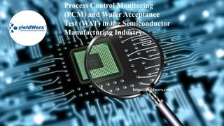
1. Process Control Monitoring
(PCM) and Wafer Acceptance
Test (WAT) in the Semiconductor
Manufacturing Industry
https://yieldwerx.com/
2. Semiconductor manufacturing is an intricate process involving numerous stages, from wafer preparation to the final packaging of the integrated
circuit. Two critical components of this process are Process Control Monitoring (PCM) and Wafer Acceptance Testing (WAT). PCM and WAT data
are crucial in verifying the quality of the wafer at the end of fabrication, identifying potential defects, and ensuring the consistent production of
high-quality semiconductor devices.
Understanding PCM
PCM Monitoring (Process Control Monitoring) refers to the control systems implemented in semiconductor manufacturing to monitor the process
parameters during wafer fabrication. The aim is to maintain the consistency of the production process, thus ensuring the desired quality and
performance of the semiconductor devices. PCM involves collecting data from the various stages of manufacturing, from deposition and etching
to photolithography and ion implantation. This data is then used to assess the integrity of the process, identify potential issues, and make
necessary adjustments to maintain statistical process control semiconductor. Different test structures are fabricated on the wafer for PCM data.
These test structures are designed to mimic the devices that will be manufactured on the wafer. By monitoring these structures, manufacturers
can assess the effects of process variations on the final device performance.
Understanding WAT
Wafer Acceptance Testing (WAT’), also known as Process Check Monitor (PCM monitor) testing, involves testing a small sample of die from each
wafer after fabrication. The purpose of WAT is to measure the electrical properties of the devices on the wafer to determine if the fabrication
process has produced devices with the desired characteristics. In WAT semiconductor, test patterns are used to exercise the device and evaluate
its performance. This testing involves applying a sequence of input signals to the device and monitoring its response. The resulting data is then
compared with expected results to determine whether the device meets the required specifications. WAT can also be used to identify process
drifts that may occur over time. By monitoring trends in the WAT data, manufacturers can detect changes in the fabrication process that might
impact device performance. Such information is essential for maintaining process control monitoring semiconductor and ensuring the consistent
quality of the devices.
3. PCM/WAT Data Analysis: Challenges and Importance
PCM and WAT data analysis is an essential but challenging aspect of semiconductor manufacturing. These datasets are vast and complex,
representing various dimensions of the manufacturing process. In addition, they're often incomplete or inconsistent due to measurement errors
or equipment malfunctions.
Despite these challenges, analyzing PCM/WAT data is vital for several reasons. Firstly, it allows manufacturers to detect defects or variations in the
manufacturing process that could lead to device failure. For example, by monitoring the data, manufacturers can identify issues such as
contamination, equipment malfunctions, or process drifts that might affect yield.
Secondly, PCM/WAT data analysis can also help improve operational efficiency. By identifying the causes of defects or pcm process variations,
manufacturers can implement corrective actions to prevent recurrence. This proactive approach can help reduce waste, improve yield, and lower
manufacturing costs.
Moreover, the STDF data analysis can also provide insights into the performance of individual devices or wafers. This information can be used to
classify the devices according to their performance, which can be beneficial in applications where high reliability is essential.
The Role of Advanced PCM/WAT Data Analysis Tools
Advanced PCM/WAT data analysis tools can play a significant role in improving the effectiveness of the analysis process. These tools can help
standardize and map data across different stages of the manufacturing process, enabling more accurate and insightful analysis. They can also
facilitate data visualization, making it easier to identify trends or anomalies.
Moreover, these tools can also integrate data from different sources, such as the wafer sort test data and final test yield data. This integration can
provide a holistic view of the manufacturing process, enabling manufacturers to identify correlations between different process parameters and
their impact on yield.
Another key advantage of advanced PCM/WAT data analysis tool is the ability to automate data analysis. With the vast amount of data generated
in semiconductor manufacturing, manual analysis is often impractical. Automation can significantly speed up the analysis process and minimize
human error, enabling more accurate and timely decision-making.
4. Conclusion
PCM and WAT data are crucial components in semiconductor manufacturing, playing a critical role in process control, quality
assurance, and operational efficiency. By effectively analyzing this data, manufacturers can detect and address potential issues,
improve yield, and ensure the consistent production of high-quality devices. The use of advanced PCM/WAT data analysis tools
can significantly enhance the effectiveness of this analysis, providing valuable insights that can drive process improvement and
cost reduction in semiconductor manufacturing.
References
1. Bader, D., and Nguyen, T. (2010). Statistical Process Control: A Tool for High-Quality Systematic Yield
Improvement. Semiconductor Manufacturing Handbook, Second Edition (pp. 13.1-13.21). McGraw Hill.
2. May, G.S., and Spanos, C.J. (2006). Fundamentals of Semiconductor Manufacturing and Process Control. John Wiley & Sons.
3. Zorzi, N., De Marchi, M., Lanza, G., Ghibaudo, G., and Ricco, B. (2015). PCM based workflow for wafer acceptance test
analysis. Microelectronic Engineering, 147, 133-136.
4. Levy, R. (2000). Process control and yield modeling in semiconductor manufacturing. World Scientific.
5. Yeh, P. (2015). Semiconductor Manufacturing Technology. Pearson.
6. SEMI. (2021). Guide to SEMI Standard for SEMI Equipment Communication Standards (SECS/GEM).
7. Kim, Y., and Kim, C. (2016). A study on the measurement system for wafer acceptance test data. Journal of Semiconductor
Technology and Science, 16(2), 227-233.