Download to read offline


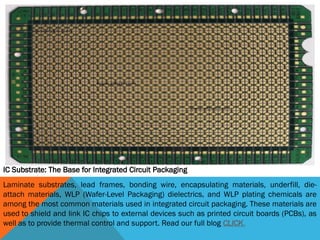
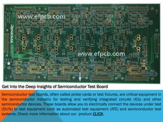
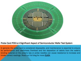
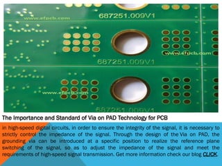


Efpcb.com offers a range of materials essential for integrated circuit packaging, including substrates, bonding wires, and dielectrics. The document also highlights the importance of semiconductor test boards for verifying integrated circuits and emphasizes the maintenance of probe cards in wafer testing to ensure accurate readings. Additionally, it discusses the significance of via on pad technology in high-speed digital circuits to maintain signal integrity.


