1. Cynthia Yu
Summer 2016
NASA Radiation Beam Degrader:
Overview:
This was the main project I worked on this past summer at NASA Johnson Space center. I worked in a small
team consisting of two mechanical engineers, to create a control system for a device called the “Beam
Degrader”.
We came up with the concept of the device together and presented it to the EV9 division who requested the
mechanism for radiation testing purposes.
This project provided exposure to many different concepts such as circuit design, schematic and PCB layout/
design using Alitum Designer, Arduino programming, along with practicing skills in soldering, bread boarding,
using the oscilloscope and power supply. I accomplished most of the goals I set out for this project as I was
able to learn more than I had hoped and advance further on the project than I had planned.
Purpose of Project: Create a portable radiation testing box containing eight moveable slides attached to 8
linear actuators of polyethylene to test electronic devices.
Constraints for design:
Limited budget of $1500 on prototype
Less than 50 pounds
Portable
Easy to use
Able to accommodate 255 different thickness combinations
Able to detect errors and display them
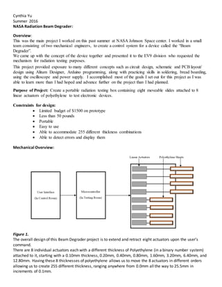
Mechanical Overview:
Figure 1.
The overall design of this Beam Degrader project is to extend and retract eight actuators upon the user’s
command.
There are 8 individual actuators each with a different thickness of Polyethylene (in a binary number system)
attached to it, starting with a 0.10mm thickness, 0.20mm, 0.40mm, 0.80mm, 1.60mm, 3.20mm, 6.40mm, and
12.80mm. Having these 8 thicknesses of polyethylene allows us to move the 8 actuators in different orders
allowing us to create 255 different thickness, ranging anywhere from 0.0mm all the way to 25.5mm in
increments of 0.1mm.
2. Figure 2.
There were many constraints for the device stated above, which was why we chose to design the device as
shown above. This square “box” design allowed NASA engineers to bring the device “on the go” to Russia and
other countries where the radiation beam was only accessible.
Figure 3.
The block diagram for the electrical configuration for the mechanism for one individual linear actuator.
3. Figure 4.
Schematic created in Altium Design for the PCB used to mount the H-bridges.
Figure 5.
The design layout of my Printed Circuit Board for the mounted H-bridges.
4. Figure 6.
Graphical User Interface designed on word for initial conceptual design.
Figure 7.
Official GUI created using LabVIEW. With all I/O’s correctly functioning.