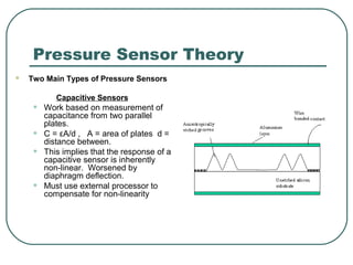
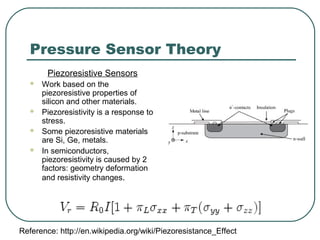
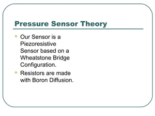
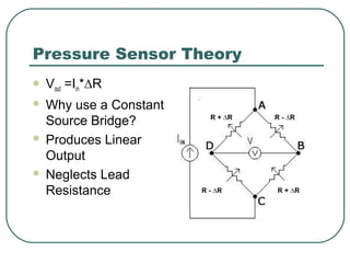
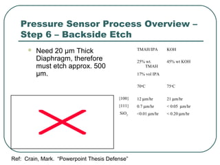
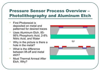
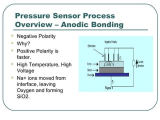
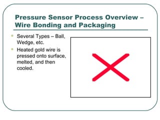
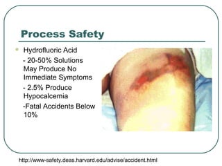
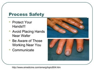
Pressure Sensor Lecture
Presentation Overview
1. Pressure Sensor Theory Overview
2. Pressure Sensor Process Overview
and Fabrication Theory Review
3. Express Safety Concerns for Particular
Processes
Pressure Sensor Theory
 Two Main Types of Pressure Sensors
Capacitive Sensors
• Work based on measurement of
capacitance from two parallel
plates.
• C = εA/d , A = area of plates d =
distance between.
• This implies that the response of a
capacitive sensor is inherently
non-linear. Worsened by
diaphragm deflection.
• Must use external processor to
compensate for non-linearity
Pressure Sensor Theory
Piezoresistive Sensors
 Work based on the
piezoresistive properties of
silicon and other materials.
 Piezoresistivity is a response to
stress.
 Some piezoresistive materials
are Si, Ge, metals.
 In semiconductors,
piezoresistivity is caused by 2
factors: geometry deformation
and resistivity changes.
Reference: http://en.wikipedia.org/wiki/Piezoresistance_Effect
Pressure Sensor Theory
 Our Sensor is a
Piezoresistive
Sensor based on a
Wheatstone Bridge
Configuration.
 Resistors are made
with Boron Diffusion.
Pressure Sensor Theory
 Vout =Iin*∆R
 Why use a Constant
Source Bridge?
 Produces Linear
Output
 Neglects Lead
Resistance
R + ∆R R - ∆R
R - ∆R R + ∆R
Pressure Sensor Process
Overview
 Initial Wafer is 525
µm thick, n-type,
<100> double-side
polished (DSP).
Pressure Sensor Process
Overview – Step 1
 What should ALWAYS be step 1?
 Wafer Cleaning (RCA Clean)
 Steps
1. TCE (Tetrachloroethylene) Immersion, Acetone, Methanol
2. Base Clean - H2O/H2O2/NH4OH (5 parts,1 part,1 part) @
70 C to Remove Organic Contaminants
3. Dilute HF Immersion (2.5%) Why?
4. Acid Clean - H2O/H2O2/HCl (4 parts, 1 part, 1 part) @ 70 C
to remove metallic and ionic contaminants.
Pressure Sensor Process
Overview – Step 2
 Any guesses?
 Thermal Oxidation
 Wet Oxidation
Followed by Dry
Oxidation
Si + O2 → SiO2 (Dry Oxidation)
Si + 2H2O2 → SiO2 (Wet Oxidation)
Pressure Sensor Process
Overview – Step 3
 Photolithography for
Piezoresistive Elements
 Contact Lithography
 Use Shipley 1813
Positive Resist
 What happens to areas
exposed to UV light in
Positive Resist?
 If we want piezoresistive
holes, do we use dark-
field or light-field mask?
Si + O2 → SiO2 (Dry Oxidation)
Si + 2H2O2 → SiO2 (Wet Oxidation)
Pressure Sensor Process
Overview – Step 3 Cont.
 DNQ Method using
Mercury Lamp
 Diazonap. Changes to
carboxylic acid via Wolf
re-arrangement
 Carboxylic Acid is more
soluble in a base than
Novolak. So exposed
areas dissolve.
 Use TMAH (a base)
mixture to develop
Ref: http://chem.chem.rochester.edu/~chem421/polymod2.htm
Pressure Sensor Process
Overview – Step 4 - Diffusion
 Creates Resistors in
Substrate
 Three Methods
1. Solid Evap. (Tetramethyl
Borate, Boron Nitride) - Rare
2. Gaseous – Diborane (B2H6) –
Dangerous!! 160 ppm for 15
min life threatening
3. Liquid – Our Type PBF-6MK –
Borosilicate polymer in
ethanol. Creates borosilicate
glass, boron oxide, and
unused boron.
5 Squares
1 Square
3Squares
Ref: Jaeger, Richard. “Introduction to Microelectronic Fabrication”
Pressure Sensor Process Overview –
Step 4 – Diffusion Continued
 What is a constant source diffusion?
 What is a limited source diffusion?
 What is drive-in?
 How can you get rid of boron oxide
and borosilicate glass?
 What additional step does this
create?
Surface
Concentration
Junction Depth
Pressure Sensor Process Overview –
Step 5 – Backside Photlithography
 Windows Must Be
Opened in New Oxide
For Backside Etch.
 Use Front to Backside
Alignment
 Etch Silicon Dioxide
w/BOE (HF 6:1)
 Finished when wafer is
hydrophobic (water rolls
off)
Pressure Sensor Process Overview –
Step 5 – Backside Photlith. Cont.
 Must Align Marks
from 1st
Mask on
Front of Wafer to
Those on Back
 What is Split Field
Alignment?
 What is a critical
dimension?
Photo:
http://www.ee.byu.edu/cleanroom/alignment.phtml
Pressure Sensor Process Overview –
Step 6 – Backside Etch
 Need 20 µm Thick
Diaphragm, therefore
must etch approx. 500
µm.
TMAH/IPA KOH
25% wt.
TMAH
45% wt KOH
17% vol IPA
70o
C 75o
C
{100} 12 µm/hr 21 µm/hr
{111} 0.7 µm/hr < 0.05 µm/hr
SiO2 <0.01 µm/hr < 0.20 µm/hr
Ref: Crain, Mark. “Powerpoint Thesis Defense”
Pressure Sensor Process Overview –
Step 7 – Pholith. For Contact
Windows
 Topside Alignment
 Use Shipley 1813
Postive Resist
Ref: Crain, Mark. “Powerpoint Thesis Defense”
Pressure Sensor Process Overview –
Step 8 Metal Deposition and Pattern
 Several Methods, we
use Sputtering
 2 Types (Magnetron)
-RF Sputter
-DC Sputter
 When do you use RF
sputter?
 What is a sputter etch?
 What is argon used? http://en.wikipedia.org/wiki/Sputtering
Pressure Sensor Process Overview –
Photolithography and Aluminum Etch
 First Photoresist is
deposited on metal and
patterned for desired traces
 Uses Aluminum Etch, 85-
95% Phosphoric Acid, 2-8%
Nitric Acid, and Water
 Why in the picture is there a
hole in the metal?
 What is the difference
between lift-off and metal
etch?
 Must Thermal Anneal After
Etch, Why?
Pressure Sensor Process
Overview – Wafer Testing
5 Squares
1 Square
3Squares
R=ρlw/xj
Rs=ρ/xj
R=(squares)ρ/xj
Contacts Equivalent: Rs=0.65 squares
Resistive Element: 6.3 squares
Pressure Sensor Process
Overview – Wafer Testing
 2 Testing Structures
 Van Der Pauw
-Contacts on Structure
Edge, Symmetrical
Rs = (π/ln 2)Vcd/Iab
 Kelvin Structures
-Used for Effective Line
Width with Rs
Weff = Iab*L*Rs/V
A B
D
C
Pressure Sensor Process
Overview – Anodic Bonding
 Negative Polarity
 Why?
 Positive Polarity is
faster.
 High Temperature, High
Voltage
 Na+ ions moved from
interface, leaving
Oxygen and forming
SiO2.
Pressure Sensor Process Overview –
Wire Bonding and Packaging
 Several Types – Ball,
Wedge, etc.
 Heated gold wire is
pressed onto surface,
melted, and then
cooled.
Process Safety
 Hydrofluoric Acid
- 20-50% Solutions
May Produce No
Immediate Symptoms
- 2.5% Produce
Hypocalcemia
-Fatal Accidents Below
10%
http://www-safety.deas.harvard.edu/advise/accident.html
Process Safety
 Protect Your
Hands!!!
 Avoid Placing Hands
Near Wafer
 Be Aware of Those
Working Near You
 Communicate
http://www.emedicine.com/emerg/topic804.htm

Pressure sensor lecture

  • 1.
  • 2.
    Presentation Overview 1. PressureSensor Theory Overview 2. Pressure Sensor Process Overview and Fabrication Theory Review 3. Express Safety Concerns for Particular Processes
  • 3.
    Pressure Sensor Theory Two Main Types of Pressure Sensors Capacitive Sensors • Work based on measurement of capacitance from two parallel plates. • C = εA/d , A = area of plates d = distance between. • This implies that the response of a capacitive sensor is inherently non-linear. Worsened by diaphragm deflection. • Must use external processor to compensate for non-linearity
  • 4.
    Pressure Sensor Theory PiezoresistiveSensors  Work based on the piezoresistive properties of silicon and other materials.  Piezoresistivity is a response to stress.  Some piezoresistive materials are Si, Ge, metals.  In semiconductors, piezoresistivity is caused by 2 factors: geometry deformation and resistivity changes. Reference: http://en.wikipedia.org/wiki/Piezoresistance_Effect
  • 5.
    Pressure Sensor Theory Our Sensor is a Piezoresistive Sensor based on a Wheatstone Bridge Configuration.  Resistors are made with Boron Diffusion.
  • 6.
    Pressure Sensor Theory Vout =Iin*∆R  Why use a Constant Source Bridge?  Produces Linear Output  Neglects Lead Resistance R + ∆R R - ∆R R - ∆R R + ∆R
  • 7.
    Pressure Sensor Process Overview Initial Wafer is 525 µm thick, n-type, <100> double-side polished (DSP).
  • 8.
    Pressure Sensor Process Overview– Step 1  What should ALWAYS be step 1?  Wafer Cleaning (RCA Clean)  Steps 1. TCE (Tetrachloroethylene) Immersion, Acetone, Methanol 2. Base Clean - H2O/H2O2/NH4OH (5 parts,1 part,1 part) @ 70 C to Remove Organic Contaminants 3. Dilute HF Immersion (2.5%) Why? 4. Acid Clean - H2O/H2O2/HCl (4 parts, 1 part, 1 part) @ 70 C to remove metallic and ionic contaminants.
  • 9.
    Pressure Sensor Process Overview– Step 2  Any guesses?  Thermal Oxidation  Wet Oxidation Followed by Dry Oxidation Si + O2 → SiO2 (Dry Oxidation) Si + 2H2O2 → SiO2 (Wet Oxidation)
  • 10.
    Pressure Sensor Process Overview– Step 3  Photolithography for Piezoresistive Elements  Contact Lithography  Use Shipley 1813 Positive Resist  What happens to areas exposed to UV light in Positive Resist?  If we want piezoresistive holes, do we use dark- field or light-field mask? Si + O2 → SiO2 (Dry Oxidation) Si + 2H2O2 → SiO2 (Wet Oxidation)
  • 11.
    Pressure Sensor Process Overview– Step 3 Cont.  DNQ Method using Mercury Lamp  Diazonap. Changes to carboxylic acid via Wolf re-arrangement  Carboxylic Acid is more soluble in a base than Novolak. So exposed areas dissolve.  Use TMAH (a base) mixture to develop Ref: http://chem.chem.rochester.edu/~chem421/polymod2.htm
  • 12.
    Pressure Sensor Process Overview– Step 4 - Diffusion  Creates Resistors in Substrate  Three Methods 1. Solid Evap. (Tetramethyl Borate, Boron Nitride) - Rare 2. Gaseous – Diborane (B2H6) – Dangerous!! 160 ppm for 15 min life threatening 3. Liquid – Our Type PBF-6MK – Borosilicate polymer in ethanol. Creates borosilicate glass, boron oxide, and unused boron. 5 Squares 1 Square 3Squares Ref: Jaeger, Richard. “Introduction to Microelectronic Fabrication”
  • 13.
    Pressure Sensor ProcessOverview – Step 4 – Diffusion Continued  What is a constant source diffusion?  What is a limited source diffusion?  What is drive-in?  How can you get rid of boron oxide and borosilicate glass?  What additional step does this create? Surface Concentration Junction Depth
  • 14.
    Pressure Sensor ProcessOverview – Step 5 – Backside Photlithography  Windows Must Be Opened in New Oxide For Backside Etch.  Use Front to Backside Alignment  Etch Silicon Dioxide w/BOE (HF 6:1)  Finished when wafer is hydrophobic (water rolls off)
  • 15.
    Pressure Sensor ProcessOverview – Step 5 – Backside Photlith. Cont.  Must Align Marks from 1st Mask on Front of Wafer to Those on Back  What is Split Field Alignment?  What is a critical dimension? Photo: http://www.ee.byu.edu/cleanroom/alignment.phtml
  • 16.
    Pressure Sensor ProcessOverview – Step 6 – Backside Etch  Need 20 µm Thick Diaphragm, therefore must etch approx. 500 µm. TMAH/IPA KOH 25% wt. TMAH 45% wt KOH 17% vol IPA 70o C 75o C {100} 12 µm/hr 21 µm/hr {111} 0.7 µm/hr < 0.05 µm/hr SiO2 <0.01 µm/hr < 0.20 µm/hr Ref: Crain, Mark. “Powerpoint Thesis Defense”
  • 17.
    Pressure Sensor ProcessOverview – Step 7 – Pholith. For Contact Windows  Topside Alignment  Use Shipley 1813 Postive Resist Ref: Crain, Mark. “Powerpoint Thesis Defense”
  • 18.
    Pressure Sensor ProcessOverview – Step 8 Metal Deposition and Pattern  Several Methods, we use Sputtering  2 Types (Magnetron) -RF Sputter -DC Sputter  When do you use RF sputter?  What is a sputter etch?  What is argon used? http://en.wikipedia.org/wiki/Sputtering
  • 19.
    Pressure Sensor ProcessOverview – Photolithography and Aluminum Etch  First Photoresist is deposited on metal and patterned for desired traces  Uses Aluminum Etch, 85- 95% Phosphoric Acid, 2-8% Nitric Acid, and Water  Why in the picture is there a hole in the metal?  What is the difference between lift-off and metal etch?  Must Thermal Anneal After Etch, Why?
  • 20.
    Pressure Sensor Process Overview– Wafer Testing 5 Squares 1 Square 3Squares R=ρlw/xj Rs=ρ/xj R=(squares)ρ/xj Contacts Equivalent: Rs=0.65 squares Resistive Element: 6.3 squares
  • 21.
    Pressure Sensor Process Overview– Wafer Testing  2 Testing Structures  Van Der Pauw -Contacts on Structure Edge, Symmetrical Rs = (π/ln 2)Vcd/Iab  Kelvin Structures -Used for Effective Line Width with Rs Weff = Iab*L*Rs/V A B D C
  • 22.
    Pressure Sensor Process Overview– Anodic Bonding  Negative Polarity  Why?  Positive Polarity is faster.  High Temperature, High Voltage  Na+ ions moved from interface, leaving Oxygen and forming SiO2.
  • 23.
    Pressure Sensor ProcessOverview – Wire Bonding and Packaging  Several Types – Ball, Wedge, etc.  Heated gold wire is pressed onto surface, melted, and then cooled.
  • 24.
    Process Safety  HydrofluoricAcid - 20-50% Solutions May Produce No Immediate Symptoms - 2.5% Produce Hypocalcemia -Fatal Accidents Below 10% http://www-safety.deas.harvard.edu/advise/accident.html
  • 25.
    Process Safety  ProtectYour Hands!!!  Avoid Placing Hands Near Wafer  Be Aware of Those Working Near You  Communicate http://www.emedicine.com/emerg/topic804.htm