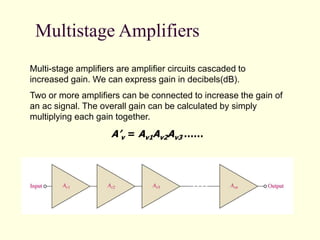
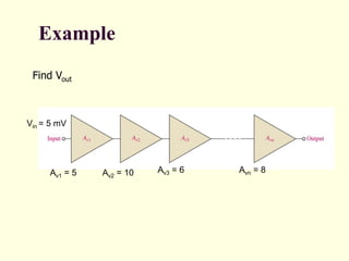
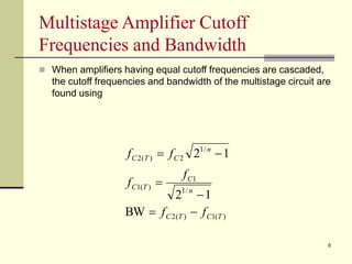
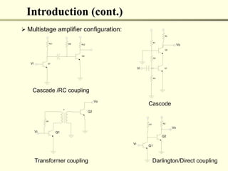
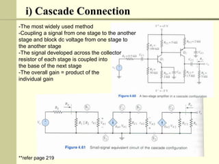
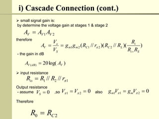
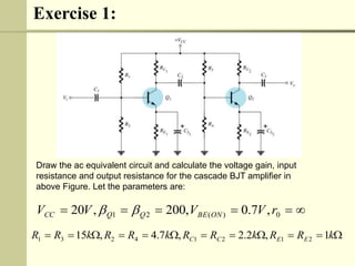
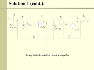
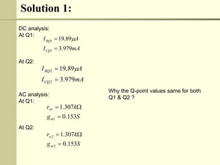
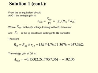
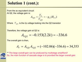
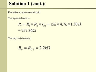
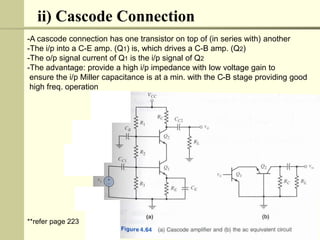
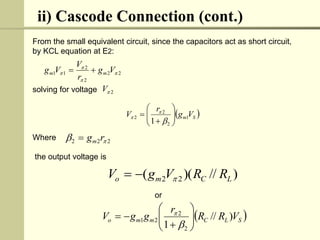
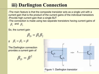
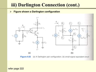
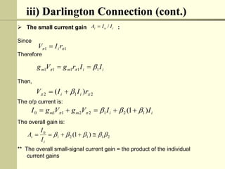
MULTISTAGE
AMPLIFIERS
Multistage Amplifiers
Two or more amplifiers can be connected to increase the
gain of an ac signal. The overall gain can be calculated by
simply multiplying each gain together.
A’v = Av1Av2Av3 ……
Introduction
 Many applications cannot be handle with single-
transistor amplifiers in order to meet the specification
of a given amplification factor, input resistance and
output resistance
 As a solution – transistor amplifier circuits can be
connected in series or cascaded amplifiers
 This can be done either to increase the overall small-
signal voltage gain or provide an overall voltage gain
greater than 1 with a very low output resistance
Multistage Amplifiers
Multi-stage amplifiers are amplifier circuits cascaded to
increased gain. We can express gain in decibels(dB).
Two or more amplifiers can be connected to increase the gain of
an ac signal. The overall gain can be calculated by simply
multiplying each gain together.
A’v = Av1Av2Av3 ……
Example
Find Vout
Av1 = 5 Av2 = 10 Av3 = 6 Avn = 8
Vin = 5 mV
6
Multistage Amplifier Cutoff
Frequencies and Bandwidth
 When amplifiers having equal cutoff frequencies are cascaded,
the cutoff frequencies and bandwidth of the multistage circuit are
found using
)
(
1
)
(
2
/
1
1
)
(
1
/
1
2
)
(
2
BW
1
2
1
2
T
C
T
C
n
C
T
C
n
C
T
C
f
f
f
f
f
f






Introduction (cont.)
 Multistage amplifier configuration:
Rc1 Rc2
RB
Vi Q1
Q2
R2
RL
R1
Vo
Vi Q1
Q2
R3
R1 R2
Vi
Vo
R1
Vi
Vo
T
Cascade /RC coupling
Cascode
Transformer coupling Darlington/Direct coupling
Q1
Q2
Q1
Q2
i) Cascade Connection
-The most widely used method
-Coupling a signal from one stage to the another
stage and block dc voltage from one stage to
the another stage
-The signal developed across the collector
resistor of each stage is coupled into
the base of the next stage
-The overall gain = product of the
individual gain
**refer page 219
i) Cascade Connection (cont.)
 small signal gain is:
by determine the voltage gain at stages 1 & stage 2
therefore
- the gain in dB
 input resistance
Output resistance
- assume ,so also
Therefore
)
)(
//
)(
//
( 2
2
1
2
1
S
i
i
L
C
C
m
m
S
o
V
R
R
R
R
R
r
R
g
g
V
V
A


 
1
2
1 //
// 
r
R
R
Ris 
0

S
V 0
2
1 
 
 V
V 0
2
1
1 
 
 V
g
V
g m
m
2
0 C
R
R 
2
1 V
V
V A
A
A 
)
log(
20
)
( V
dB
V A
A 
Exercise 1:
Draw the ac equivalent circuit and calculate the voltage gain, input
resistance and output resistance for the cascade BJT amplifier in
above Figure. Let the parameters are:











 k
R
R
k
R
R
k
R
R
k
R
R E
E
C
C 1
,
2
.
2
,
7
.
4
,
15 2
1
2
1
4
2
3
1





 0
)
(
2
1 ,
7
.
0
,
200
,
20 r
V
V
V
V ON
BE
Q
Q
CC 

Solution 1 (cont.):
2
1
1
// R
R
RB

1

r


1

V


2

V 2

r
2
C
R
1
C
R
1
1 
V
gm
2
2 
V
gm
4
3
2
// R
R
RB

i
V
0
V
1
B 2
B
1
E
1
C
2
E
2
C
i
R
0
R
Ac equivalent circuit for cascade amplifier
Solution 1:
DC analysis:
At Q1:
At Q2:
AC analysis:
At Q1:
At Q2:
S
g
k
r
m 153
.
0
307
.
1
1
1




Why the Q-point values same for both
Q1 & Q2 ?
mA
I
A
I
CQ
BQ
979
.
3
89
.
19
1
1

 
S
g
k
r
m 153
.
0
307
.
1
2
2




mA
I
A
I
CQ
BQ
979
.
3
89
.
19
2
2

 
Solution 1 (cont.):
From the ac equivalent circuit:
At Q1, the voltage gain is:
Where is the o/p voltage looking to the Q1 transistor
and is the i/p resistance looking into Q2 transistor
Therefore
The voltage gain at Q1 is:
2
i
R
1
0Q
V
)
//
( 2
1
1
0
1 i
C
m
Q
VQ R
R
g
Vi
V
A 


06
.
102
)
36
.
957
//
2
.
2
(
153
.
0
1 


 k
AVQ



 36
.
957
307
.
1
//
7
.
4
//
15
// 2
2
2 k
k
k
r
R
R B
i 
Solution 1 (cont.):
From the ac equivalent circuit:
At Q2, the voltage gain is:
Where is the i/p voltage looking into the Q2 transistor
Therefore, the voltage gain at Q2 is:
The overall gain is then,
** The large overall gain can be produced by multistage amplifiers!!
So, the main function of cascade stage is to provided the larger overall gain
2
iQ
V
)
( 2
2
0
2 C
m
iQ
VQ R
g
V
V
A 


6
.
336
)
2
.
2
(
153
.
0
2 


 k
AVQ
353
,
34
)
6
.
336
)(
06
.
102
(
2
1 



 VQ
VQ
V A
A
A
Solution 1 (cont.):
From the ac equivalent circuit:
The i/p resistance is:
The o/p resistance is:




36
.
957
307
.
1
//
7
.
4
//
15
//
// 1
2
1 k
k
k
r
R
R
Ri 


 k
R
R C
o 2
.
2
2
ii) Cascode Connection
-A cascode connection has one transistor on top of (in series with) another
-The i/p into a C-E amp. (Q1) is, which drives a C-B amp. (Q2)
-The o/p signal current of Q1 is the i/p signal of Q2
-The advantage: provide a high i/p impedance with low voltage gain to
ensure the i/p Miller capacitance is at a min. with the C-B stage providing good
high freq. operation
**refer page 223
ii) Cascode Connection (cont.)
From the small equivalent circuit, since the capacitors act as short circuit,
by KCL equation at E2:
solving for voltage
Where
the output voltage is
or
2
2
2
2
1
1 


 V
g
r
V
V
g m
m 

2

V
 
S
m V
g
r
V 1
2
2
2
1 












2
2
2 
 r
gm

)
//
)(
( 2
2 L
C
m
o R
R
V
g
V 


 
S
L
C
m
m
o V
R
R
r
g
g
V )
//
1 2
2
2
1 












ii) Cascode Connection (cont.)
Therefore the small signal voltage gain:
From above equation shows that:
So, the cascode gain is the approximately
* The gain same as a single-stage C-E amplifier
 
L
C
m
m
S
V R
R
r
g
g
V
V
A //
1 2
2
2
1
0














 
L
C
m
V R
R
g
A //
1


1
1
1 2
2
2
2
2 










 



r
gm
iii) Darlington Connection
-The main feature is that the composite transistor acts as a single unit with a
current gain that is the product of the current gains of the individual transistors
-Provide high current gain than a single BJT
-The connection is made using two separate transistors having current gains of
and
So, the current gain
If
The Darlington connection
provides a current gain of
2
1

 
D
1
 2



 
 2
1
2

 
D
Figure 1: Darlington transistor
iii) Darlington Connection (cont.)
 Figure shown a Darlington configuration
refer page 222
iii) Darlington Connection (cont.)
 The small current gain :
Since
Therefore
Then,
The o/p current is:
The overall gain is:
** The overall small-signal current gain = the product of the individual
current gains
i
i
m
m I
I
r
g
V
g 1
1
1
1
1 

 

2
1
2 )
( 
  r
I
I
V i
i 

i
i
m
m I
I
V
g
V
g
I )
1
( 1
2
1
2
2
1
1
0 



 




2
1
1
2
1
0
)
1
( 



 




i
i
I
I
A
i
o
i I
I
A /

1
1 
 r
I
V i

iii) Darlington Connection (cont.)
 The input resistance:
Known that:
So, the i/p resistance is:
The base of Q2 is connnected to the emitter of Q1, which means that the i/p
resistance to Q2 is multiplied by the factor , as we saw in
circuits with emitter resistor.
So, we can write: and
Therefore
The i/p resistance is then approximately
**The i/p resistance tends to be large because of the multiplication
2
1
1
2
1 )
1
( 


  r
I
r
I
V
V
V i
i
i 




2
1
1 )
1
( 
  r
r
Ri 


1
1
CQ
T
I
V
r

 
2
2
1

CQ
CQ
I
I 
2
1
2
2
1
1 
 

 r
I
V
r
CQ
T










2
1
2 
 r
Ri 
)
1
( 1




multistage amplifiers analysis and design

  • 1.
  • 2.
    Multistage Amplifiers Two ormore amplifiers can be connected to increase the gain of an ac signal. The overall gain can be calculated by simply multiplying each gain together. A’v = Av1Av2Av3 ……
  • 3.
    Introduction  Many applicationscannot be handle with single- transistor amplifiers in order to meet the specification of a given amplification factor, input resistance and output resistance  As a solution – transistor amplifier circuits can be connected in series or cascaded amplifiers  This can be done either to increase the overall small- signal voltage gain or provide an overall voltage gain greater than 1 with a very low output resistance
  • 4.
    Multistage Amplifiers Multi-stage amplifiersare amplifier circuits cascaded to increased gain. We can express gain in decibels(dB). Two or more amplifiers can be connected to increase the gain of an ac signal. The overall gain can be calculated by simply multiplying each gain together. A’v = Av1Av2Av3 ……
  • 5.
    Example Find Vout Av1 =5 Av2 = 10 Av3 = 6 Avn = 8 Vin = 5 mV
  • 6.
    6 Multistage Amplifier Cutoff Frequenciesand Bandwidth  When amplifiers having equal cutoff frequencies are cascaded, the cutoff frequencies and bandwidth of the multistage circuit are found using ) ( 1 ) ( 2 / 1 1 ) ( 1 / 1 2 ) ( 2 BW 1 2 1 2 T C T C n C T C n C T C f f f f f f      
  • 7.
    Introduction (cont.)  Multistageamplifier configuration: Rc1 Rc2 RB Vi Q1 Q2 R2 RL R1 Vo Vi Q1 Q2 R3 R1 R2 Vi Vo R1 Vi Vo T Cascade /RC coupling Cascode Transformer coupling Darlington/Direct coupling Q1 Q2 Q1 Q2
  • 8.
    i) Cascade Connection -Themost widely used method -Coupling a signal from one stage to the another stage and block dc voltage from one stage to the another stage -The signal developed across the collector resistor of each stage is coupled into the base of the next stage -The overall gain = product of the individual gain **refer page 219
  • 9.
    i) Cascade Connection(cont.)  small signal gain is: by determine the voltage gain at stages 1 & stage 2 therefore - the gain in dB  input resistance Output resistance - assume ,so also Therefore ) )( // )( // ( 2 2 1 2 1 S i i L C C m m S o V R R R R R r R g g V V A     1 2 1 // //  r R R Ris  0  S V 0 2 1     V V 0 2 1 1     V g V g m m 2 0 C R R  2 1 V V V A A A  ) log( 20 ) ( V dB V A A 
  • 10.
    Exercise 1: Draw theac equivalent circuit and calculate the voltage gain, input resistance and output resistance for the cascade BJT amplifier in above Figure. Let the parameters are:             k R R k R R k R R k R R E E C C 1 , 2 . 2 , 7 . 4 , 15 2 1 2 1 4 2 3 1       0 ) ( 2 1 , 7 . 0 , 200 , 20 r V V V V ON BE Q Q CC  
  • 11.
    Solution 1 (cont.): 2 1 1 //R R RB  1  r   1  V   2  V 2  r 2 C R 1 C R 1 1  V gm 2 2  V gm 4 3 2 // R R RB  i V 0 V 1 B 2 B 1 E 1 C 2 E 2 C i R 0 R Ac equivalent circuit for cascade amplifier
  • 12.
    Solution 1: DC analysis: AtQ1: At Q2: AC analysis: At Q1: At Q2: S g k r m 153 . 0 307 . 1 1 1     Why the Q-point values same for both Q1 & Q2 ? mA I A I CQ BQ 979 . 3 89 . 19 1 1    S g k r m 153 . 0 307 . 1 2 2     mA I A I CQ BQ 979 . 3 89 . 19 2 2   
  • 13.
    Solution 1 (cont.): Fromthe ac equivalent circuit: At Q1, the voltage gain is: Where is the o/p voltage looking to the Q1 transistor and is the i/p resistance looking into Q2 transistor Therefore The voltage gain at Q1 is: 2 i R 1 0Q V ) // ( 2 1 1 0 1 i C m Q VQ R R g Vi V A    06 . 102 ) 36 . 957 // 2 . 2 ( 153 . 0 1     k AVQ     36 . 957 307 . 1 // 7 . 4 // 15 // 2 2 2 k k k r R R B i 
  • 14.
    Solution 1 (cont.): Fromthe ac equivalent circuit: At Q2, the voltage gain is: Where is the i/p voltage looking into the Q2 transistor Therefore, the voltage gain at Q2 is: The overall gain is then, ** The large overall gain can be produced by multistage amplifiers!! So, the main function of cascade stage is to provided the larger overall gain 2 iQ V ) ( 2 2 0 2 C m iQ VQ R g V V A    6 . 336 ) 2 . 2 ( 153 . 0 2     k AVQ 353 , 34 ) 6 . 336 )( 06 . 102 ( 2 1      VQ VQ V A A A
  • 15.
    Solution 1 (cont.): Fromthe ac equivalent circuit: The i/p resistance is: The o/p resistance is:     36 . 957 307 . 1 // 7 . 4 // 15 // // 1 2 1 k k k r R R Ri     k R R C o 2 . 2 2
  • 16.
    ii) Cascode Connection -Acascode connection has one transistor on top of (in series with) another -The i/p into a C-E amp. (Q1) is, which drives a C-B amp. (Q2) -The o/p signal current of Q1 is the i/p signal of Q2 -The advantage: provide a high i/p impedance with low voltage gain to ensure the i/p Miller capacitance is at a min. with the C-B stage providing good high freq. operation **refer page 223
  • 17.
    ii) Cascode Connection(cont.) From the small equivalent circuit, since the capacitors act as short circuit, by KCL equation at E2: solving for voltage Where the output voltage is or 2 2 2 2 1 1     V g r V V g m m   2  V   S m V g r V 1 2 2 2 1              2 2 2   r gm  ) // )( ( 2 2 L C m o R R V g V      S L C m m o V R R r g g V ) // 1 2 2 2 1             
  • 18.
    ii) Cascode Connection(cont.) Therefore the small signal voltage gain: From above equation shows that: So, the cascode gain is the approximately * The gain same as a single-stage C-E amplifier   L C m m S V R R r g g V V A // 1 2 2 2 1 0                 L C m V R R g A // 1   1 1 1 2 2 2 2 2                 r gm
  • 19.
    iii) Darlington Connection -Themain feature is that the composite transistor acts as a single unit with a current gain that is the product of the current gains of the individual transistors -Provide high current gain than a single BJT -The connection is made using two separate transistors having current gains of and So, the current gain If The Darlington connection provides a current gain of 2 1    D 1  2       2 1 2    D Figure 1: Darlington transistor
  • 20.
    iii) Darlington Connection(cont.)  Figure shown a Darlington configuration refer page 222
  • 21.
    iii) Darlington Connection(cont.)  The small current gain : Since Therefore Then, The o/p current is: The overall gain is: ** The overall small-signal current gain = the product of the individual current gains i i m m I I r g V g 1 1 1 1 1      2 1 2 ) (    r I I V i i   i i m m I I V g V g I ) 1 ( 1 2 1 2 2 1 1 0           2 1 1 2 1 0 ) 1 (           i i I I A i o i I I A /  1 1   r I V i 
  • 22.
    iii) Darlington Connection(cont.)  The input resistance: Known that: So, the i/p resistance is: The base of Q2 is connnected to the emitter of Q1, which means that the i/p resistance to Q2 is multiplied by the factor , as we saw in circuits with emitter resistor. So, we can write: and Therefore The i/p resistance is then approximately **The i/p resistance tends to be large because of the multiplication 2 1 1 2 1 ) 1 (      r I r I V V V i i i      2 1 1 ) 1 (    r r Ri    1 1 CQ T I V r    2 2 1  CQ CQ I I  2 1 2 2 1 1      r I V r CQ T           2 1 2   r Ri  ) 1 ( 1   