Downloaded 74 times

![222 Cmo RvgV π−=
22
2
2 Cm
o
Rg
v
V
A −==
π
( )221112 //// πππ rRRvgv BCm−=
[ ]iVv =1π
( )2212
2
1 //// π
π
rRRg
V
v
A BCm
i
−==
( )2211 //// πrRRVg BCim−=
17](https://image.slidesharecdn.com/ecaunit2-190223145747/85/Eca-unit-2-17-320.jpg)
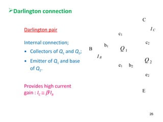
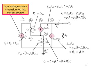
![Currents in darlington pair
Q 1
Q 2
β 1Ι Β 1
Ι Β 1
Ι E 1 = (1+β 1)Ι Β 1 = Ι Β 2
Ι E 2 = (1+β 2)Ι Β 2 =(1+β 1)(1+β 2)Ι Β 1
Ι C 2 = β 2Ι Β 2 =β 2(1+β 1)Ι Β 1
Ι C 1 + ΙC 2 = [β 1 + β 2(1+β 1)]Ι Β 1
27](https://image.slidesharecdn.com/ecaunit2-190223145747/85/Eca-unit-2-27-320.jpg)
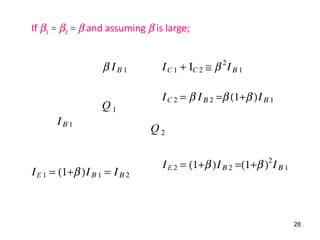
![[ ]
( )2100225.203
2.2100100100 2
×++
++
−=vA V/V4.55−=vA
Substituting values;
44
Simplifying;
( )[ ]
( ) 211
211
1
1
ππ β
βββ
rr
R
v
v
A C
s
o
v
++
++
−==](https://image.slidesharecdn.com/ecaunit2-190223145747/85/Eca-unit-2-44-320.jpg)
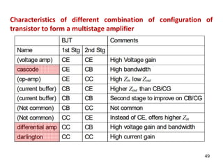

The document provides an in-depth overview of multistage amplifiers in electronic circuit analysis, detailing configurations like cascade, cascode, and Darlington arrangements with examples. It discusses the calculation of overall gain from interconnected amplifiers and includes references for further study. Key aspects covered are design principles, output resistance, input resistance, and small-signal voltage gain calculations for these amplifier configurations.