Qorvo QPF4006 39GHz GaN MMIC Front End Modulesystem_plus
The first MMIC FEM targeting 5G base stations and terminals using a 0.15µm GaN-on-SiC process.
More information on that report at: https://www.systemplus.fr/reverse-costing-reports/qorvo-qpf4006-39ghz-gan-mmic-front-end-module/
Status of the Power Electronics Industry 2017 Report by Yole Developpement Yole Developpement
Power devices fuel and enable industry mega trends reaching almost US$35B in 2022.
SOLAR AND ELECTRIC VEHICLE POWER CONVERTER MARKETS GREW SPECTACULARLY – BY MORE THAN 20% – LAST YEAR, DRIVING GROWTH IN THE EXPANDING IGBT MARKET
The power electronics sectors continue to expand their presence almost everywhere. Renewable energies and e-mobility, including electric and hybrid vehicles (EV/HEVs), are especially boosting this market. Both the solar and EV/HEV converter markets grew by over 20% between 2015 and 2016. At the semiconductor level, the power semiconductor market grew by 3.8% compared to 2015. This year, Yole Développement has enlarged its power semiconductor market analysis to all types of power integrated circuits (ICs) including power management ICs, linear regulators and switching regulators, representing a total market of $28B. Among all the different types of power devices including thyristors, MOSFETs, IGBTs and power ICs, IGBTs made the greatest progress, with around 8% growth.
Yole Développement’s decision to start analyzing the power IC market evolution closely is part of an effort to cover the whole power spectrum of this market. We now encompass the complete range from low power, low voltage, highly integrated power management ICs in mobile phones to more robust, high power IGCT modules used in trains.
The report also covers the fast-emerging wide band gap (WBG) semiconductor market, identifying today and tomorrow’s leading silicon carbide (SiC) and gallium nitride (GaN) players and the key technological details. ‘Status of Power Electronics Industry 2017 (SPEI 2017)’ describes the evolution and forecasts the future of the power inverter, power device and silicon wafer markets.
2. 58 Fundamentals Review Vol.3 No.1
ように,ノードの電位をニュートン法によって求める数値計
算ソフトといえる.
過渡解析では,単に電流だけでなく外部電圧によって誘起
される電荷も電流応答にかかわってくる.これを記述してい
る物理式は,電流連続方程式から導かれ,一般には下記のよ
うに記述する
a0
a a0
d
d
Q
I t I t
t
(1)
ここで大事な役割を果たすのが,与えられた電圧に対してど
れだけ電流が流れるか,またどれだけ電荷を誘起するかを記
述したモデル式,いわゆる回路モデルということが分かる.
回路モデルの精度が設計を正確に予測するための鍵を握る.
3.Meyerモデル
MOSFETの模式図を図2
(a)
に示す.ゲート,
ソース,
ドレー
ン,バルクの4端子からなり,ゲート電圧Vgs を変化させるこ
とによって酸化膜下に蓄えられる電荷の量を変え,ドレーン
電圧Vds をかけることによって,これをドレーン電極に取り
込む仕組みになっている.世界初のMOSFET用回路モデル,
Meyerモデルでは図2
(b)
に示すように,MOSFET内を流れる
ドレーン電流Ids と主なキャパシタンスから構成されている.
それは,式
(1)
を
a0
a a0
G,S,D,B
d
d
b
b b
Q V
I t I t
V t
(2)
と記述していることによる.ここで電流式にはドリフト近似
が用いられており,キャリヤはソースとドレーンにかかる電
場によって流れるとして,Ids の解析式が導かれている.
ds
d
I W qn
dy
(3)
ここでポテンシャルφはソースからドレーンまで外部電圧に
よって変化する量である.ポテンシャルはソース端ではゼロ,
チャネルの終わりではドレーン電圧と等しくなると仮定し,
ガウスの法則
ox ox Si Si S
E E Q
(4)
を適用すると,有名なSahの式
(3)
2
ds ox th ds ds
1
2
gs
W
I C V V V V
L
(5)
が導ける.これがMeyerモデルの基になり,BSIMでも踏襲
されているドリフト電流式である.
ここで明らかになってくることは,式(5)はVds の負の二次
関数なので,Vds が大きくなるとIds が減少してくることであ
る.もう一つの問題はこの式では,Vgs がしきい値電圧Vth に
達したら電流が流れ始めることである.このため,この記述
法をしきい値電圧モデルとも呼ばれる.
実際には図3に示すように,サブスレッショルド領域でも
微小ながら電流は流れる.
図3に示すように,ドリフトモデルは強反転領域のみに有
効で,サブスレッショルド領域や弱反転領域では破たんして
いる.これを補うためにBSIMでは別の式をスムーズにつな
げて,すべての電圧について拡張している.このしきい値電
圧モデルは世界中で広く使われている.それは,デバイス特
性が外部電圧の関数で記述されているため,特性そのものを
容易に予測することができることによる.しかし問題として
は,ドリフト近似という強反転領域のみに有効な式を拡張し
ているので,必然的にモデルパラメータと呼ばれる,実測値
を再現するためのフィッティングパラメータが増え続けてい
ることと,式をつなぎ合わせているため,高次の微分に不連
続が生じる等の問題が顕著になってきていることが挙げられ
る.
回路の低電圧動作の実現には,動作電圧を下げると同時に,
しきい値電圧を下げる必要がある.更に強反転領域から弱反
転領域を使うことになってくる.一般にアナログ回路は主に
弱反転領域を用いて設計される.この領域ではドリフトモデ
ルはもはや有効ではなく,電流からキャパシタンスに至るす
べてのMOSFET特性を正確に記述することは困難になってく
ることが容易に想像される.
(a)
(b)
図2 MeyerモデルのMOSFET記述
図 3 ドレーン電流Ids のゲート電圧Vgs 依存性 サブスレッ
ショルド領域ではドリフト項ではなく拡散項が支配する.
3. 59
Fundamentals Review Vol.3 No.1
シャルを図6に示すように,それぞれφS0,φSL と呼ぶ.
回路シミュレーションではデバイス内の情報はなく,それ
ぞれのノードでの情報として認識する.したがって,電荷は
チャネル内電荷分布をチャネル内,つまりy について積分す
ることによって得られる.また,反転層電荷と,キャリヤ速
度の積をチャネルに沿って積分するとチャネル内を流れる電
4.表面ポテンシャルモデル
デバイスの基本方程式を表1に記す.ポアソン方程式は,
ポテンシャルとキャリヤ濃度の関係を記述する.第2の方程
式は,電流密度が電界によって支配されるドリフト項とキャ
リヤ濃度のこう配によって支配される拡散項によって記述で
きることを示す.第3式の電流連続方程式は過渡応答を記述
しており,式(1)の形で回路シミュレータSPICEが解く.し
たがって回路モデルとは,
電流,
電荷,
キャパシタンスという,
いわゆるデバイス特性の電圧特性を解析的に記述したものと
いえる.
図4にこれらの式に含まれるポテンシャルφをMOSFETの
深さ方向の関数として示す.特に表面のポテンシャルφの値
を表面ポテンシャルφs と呼ぶ.
図5にポテンシャルがこう配を持つことによって誘起され
る電荷を示す.反転層電荷Qi は表面から数nmのところに形
成される反転層内に集まっている.この厚さはチャネル長と
比べると無視できるとしてデバイス特性の解析式を導く.こ
れをcharge-sheet近似と呼ばれる(7)
.これに反して空乏層電荷
Qb は表面ポテンシャルφs の関数で広がっていく.
それぞれの電荷はチャネル方向の表面ポテンシャルφs(y)
の関数として記述できる.表面ポテンシャルφs は,ポアソン
方程式と式(4)とガウスの法則から導かれる以下の式
(6)
を解いて得られる.ここでφf は擬フェルミを表し,ソース
端でゼロ,ドレーン端でドレーン電圧 Vds となる.gradual
channel近似,すなわちチャネル方向のポテンシャル変化は,
深さ方向のポテンシャル変化に比べると緩やかと仮定する
と,ポアソン方程式はソース端とドレーン端とで独立にチャ
ネルの深さ方向のみに対して解けばよいことになる.上式
をソース端とドレーン端で別々に解いて得られる表面ポテン
D A
i
n
p
n p
n p
n
: :
:
: :
:
: MOS
: MOS
: :
: :
: :
: :
:
Si
q
N N
n
n
p
n p
k T
j j
D D
ポテンシャル 電子の電荷
シリコンの誘導率
ドーナー濃度 アクセプター濃度
真性シリコンキャリア濃度
のフェルミポテンシャル
のフェルミポテンシャル
電子濃度 ホール濃度
ボルツマン定数 絶対温度
電子の電流密度 ホールの電流密度
電子の移動度 ホールの移動度
電子の拡散係数 p
0
:
: :DC
: :
I I
Q t
ホールの拡散係数
電流; 電流
誘起電荷密度 時間
図4 MOSFETの深さ方向のポテンシャル分布 表面ポテン
シャルφS の定義を示す.
図5 MOSFETの深さ方向のポテンシャル分布とこれによって誘
起される電荷 Qi:反転層電荷;Qb:空乏層電荷;Qg:ゲー
ト電荷.
図6 チャネル方向のポテンシャル分布のうちで基本的デバイス
特性を記述するために必要な二つのポテンシャルを示す ソー
ス端のポテンシャルφS0;ドレーン端φSL.
表1 デバイスの基本方程式
D
i
n
p
n
n
n
:
:
:
:
: MOS
: MOS
:
:
:
:
:
:
:
Si
N
n
n
p
n
k
j
D
I
Q
�
�
�
�
�
�������������
��������
������������
������������
�����������
�����������
���������������
�����������
����������
����������
��������
��������������
���������
A
p
p
p
0
:
:
:
:
:
:
:
:DC
:
q
N
p
T
j
D
I
t
�
�����
��������
�����
����
��������
�������
��������
��
��
8. 64 Fundamentals Review Vol.3 No.1
6.おわりに
MOSFETの微細化は様々の恩恵をもたらす.
しかし同時に,
好ましくない特性が顕著になってきており,回路シミュレー
ションを用いた性能予測が重要になってきている.これには,
高精度回路モデルが要求されることになり,従来のMeyerモ
デルでは不十分になってきた.これに伴って,物理原理に基
づく表面ポテンシャルモデルへの進化を余儀なくされてき
た.この両者のモデルの違いを明らかにし,表面ポテンシャ
ルモデルでは,デバイス特性がその原理に基づいて記述でき
ることを解説した.
(平成21年5月7日受付 平成21年5月27日最終受付)
文 献
(1) B. Razavi, “CMOS technology characterization for analog and RF
design,” IEEE J. Solid-State Circuits, vol.34,no.3, pp.268-276,
March 1999.
(2) J. E. Meyer, “MOS models and circuit simulation,” RCA Rev., vol.
32, pp. 42-63, March 1971.
(3) C. T. Sah, “Characteristics of the metal-oxide semiconductor
transistors,” IEEE Trans. Electron Devices, vol. 11, no.7, pp.
324-345, July 1964.
(4) BSIM 4.0.0 MOSFET Model, Userʼ s Manual, Department of
Electrical Engineering and Computer Science, University of
California, Berkeley California, 2000.
(5) M. M.-Mattausch, U. Feldmann, A. Rahm, M. Bollu, and D.
Savignac, “Unified Complete MOSFET model for analysis of
digital and analog circuits,” IEEE Trans. comput.-Aided Des. Integr.
Circuits Syst., vol.15, no. 1, pp.1-7, Jan. 1996.
(6) L. W. Nagel, SPICE2: A computer program to simulate
semiconductor circuits, Memorandum No. UCB/ERL-MS20,
Electronic Res. Lab., University of California, Berkeley, May 1975.
(7) J. R. Brews, “A charge-sheet model of the MOSFET,” Solid. State
Electron., vol. 21, pp. 345-355, 1978.
(8) M. M.-Mattausch, H. J. Mattausch and T. Ezaki, The Physics And
Modeling of MOSFETs: Surface-potential model HiSim, World
Scientific Pub. Co. Inc., Singapore, 2008.
(9) M.M.-Mattausch, N. Sadachika, D. Navarro, G. Suzuki, Y. Takeda,
M. Miyake, T. Warabino, Y. Mizukane, R. Inagaki, T. Ezaki, H. J.
Mattausch, T. Ohguro, T. Iizuka, M. Taguchi, S. Kumashiro, and
S. Miyamoto, “HiSIM2: Advanced MOSFET model valid for RF
circuit simulation,” IEEE Trans. Electron Devices, vol.53, no.9, pp.
1994-2007, Sept. 2006.
(10)H. J. Mattausch, M. Miyake, T. Yoshida, S. Hazama, D. Navarro,
N. Sadachika, T.Ezaki, and M. M.-Mattausch, “HiSIM2 ciruit
simulation,” IEEE Circuits Devices Mag., vol.22, no.5, pp.29-38,
Sept./Oct. 2006.
(11)H. Kawano, M. Nishizawa, S. Matsumoto, S. Mitani, M. Tanaka,
N. Nakayama, H. Ueno, M. M.-Mattausch, and H. J. Mattausch, “A
practical small-signal equivalent circuit model for RF-MOSFETs
valid up to the cut-off frequency,” IEEE Int. Microwave Sym.
Digest, pp. 2121-2124, June 2002.
(12)D. Navarro, Y. Takeda, M. Miyake, N. Nakayama, K. Machida, T.
Ezaki, H. J. Mattausch and M. M.-Mattausch, “A carrier-transit-
delay-based nonquasi-static MOSFET model for circuit simulation
and its application harmonic distortion analysis,” IEEE Trans.
Electron Devices, vol. 53, no. 9, pp. 2025-2034, September 2006.
(13)S. Jinbou, H. Ueno, H. Kawano, K. Morikawa, N. Nakayama, M.
M.-Mattausch, and H. J. Mattausch, “Analysis of non-quasistatic
contribution to small-signal response for deep sub-um MOSFET
technologies,” Ext. Abs. Int. Conf. Solid-State Devices and
Materials, pp. 26-27, Nagoya, Sept. 2002.
(14)Y. Takeda, D. Navarro, S. Chiba, M. M.-Mattausch, H. J. Mattausch,
T. Ohguro, T. Iizuka, M. Taguchi,S. Kumashiro, and S. Miyamoto,
“MOSFET harmonic distortion analysis up to the non-quasi-
static frequency regime,” The IEEE Custom Integrated Circuits
Conference, pp. 827-830, San Jose, Sept. 2005.
(15)S. Matsumoto, H. Ueno, S. Hosokawa, T. Kitamura, M. M.-
Mattausch, H. J. Mattausch, T. Ohguruo,S. Kumashiro, T.
Yamaguchi, K. Yamashita and N. Nakayama, “1/f-noise
characteristics in 100nm-MOSFETs and its modeling for circuit
simulation,” IEICE Trans. Electron., vol. E88-C, no.2, pp. 247-254,
Feb. 2005.
(16)S. Hosokawa, D. Navarro, M. M.-Mattausch, and H. J. Mattausch,
“Gate-length and drain-voltage dependence of thermal drain noise
in advanced metal-oxide-semiconductor-field-effect transistors,”
Appl. Phys. Lett., vol.87, 092104, Aug. 2005.
(17)T. Warabino, M. Miyake, D. Navarro, Y. Takeda, G. Suzuki, T.
Ezaki, M. M.-Mattausch, H. J. Mattausch, T. Ohguro, T. Iizuka, M.
Taguchi, S. Kumashiro, and S. Miyamoto, “Analysis and compact
(a)
(b) (c)
図21 代表的なMOSFETで観測されるノイズの測定値とHiSIMの計算結果の比較
9. 65
Fundamentals Review Vol.3 No.1
modeling of MOSFET high-frequency noise,” International
Conference on Simulation of Semiconductor Processes and Devices,
pp. 158-161, Monterey, Sept. 2006.
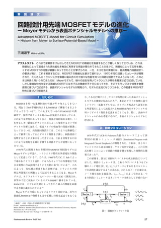
三浦道子
(正員)
1980広島大大学院博士課程了,理博.1981ドイツ,
マックス・プランク固体物理学研究所研究員,1984
シーメンス中央研究所入社.主管研究員を経て1996
広島大・工・教授.改組により1998広島大大学院先
端物質科学研究科極微微細デバイス工学研究室教授.
HiSIM 研究センター,センター長,IEEE フェロー,
Distinguished Lecturer.