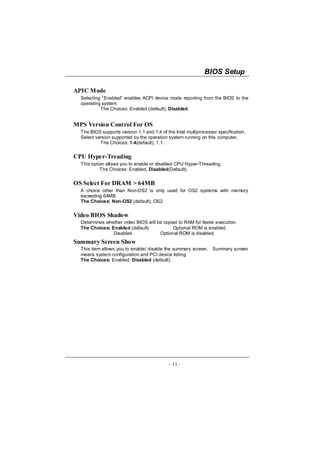
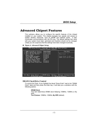
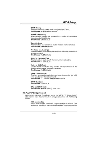
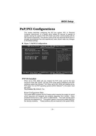
Downloaded 50 times


![Motthe rboa r d D e sc riipttiion
Mo he rboa r d D e sc r p on
Chapter 3: WarpSpeeder™
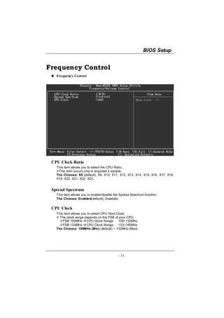
3.1 Introduction
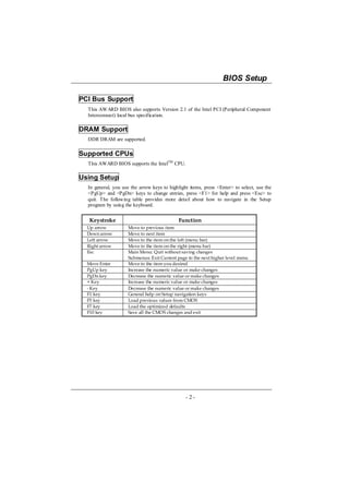
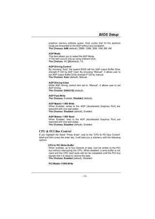
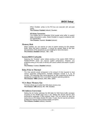
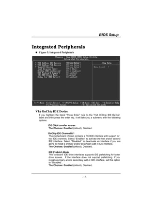
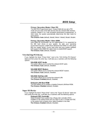
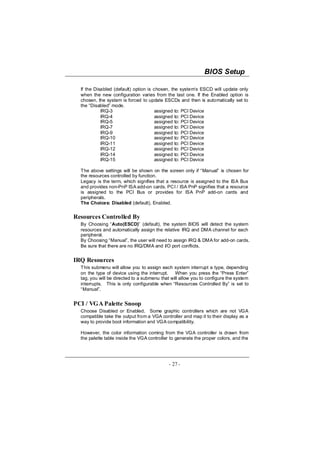
[Warp Sp eeder™], a new p owerful control utility, features three
user-friendly functions includin g Overclock M anager, Overvoltage
M anager, and Hardware Monitor.
With the Overclock M anager, users can easily adjust the frequency
they p refer or they can get the best CPU p erformance with just one
click. The Overvoltage Manager, on the other hand, help s to p ower
up CPU core voltage and M emory voltage. The cool Hardware
M onitor smartly indicates the temp eratures, voltage and CPU fan
sp eed as well as the chip set information. Also, in the About p anel,
y ou can get detail descriptions about BIOS model and chip sets. In
addition, the frequency status of CPU, memory, AGP and PCI along
with the CPU sp eed are sy nchronically shown on our main p anel.
M oreover, to p rotect users' computer sy stems if the setting is not
approp riate when testing and results in sy stem fail or han g,
[Warp Sp eeder™] technology assures the sy stem stability by
automatically rebooting the co mputer and then restart to a sp eed that
is either the original sy stem sp eed or a suitable one.
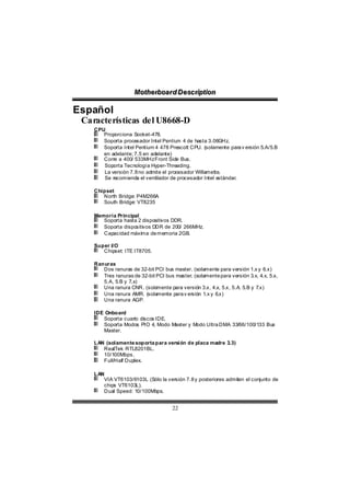
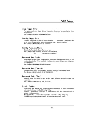
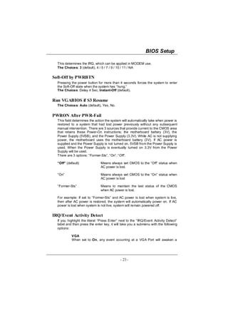
3.2 S ystem Requirement
OS Sup p ort: Windows 98 SE, Windows M e, Windows 2000,
Windows XP
DirectX: DirectX 8.1 or above. (The Windows XP op erating system
includes DirectX 8.1. If you use Windows XP, you do not need to
28](https://image.slidesharecdn.com/8668d0629cb-130416194731-phpapp02/85/Manual-de-tarjeta-madre-U8668-28-320.jpg)
![Motthe rboa r d D e sc riipttiion
Mo he rboa r d D e sc r p on
install DirectX 8.1.)
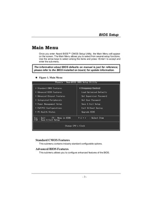
3.3 Installation
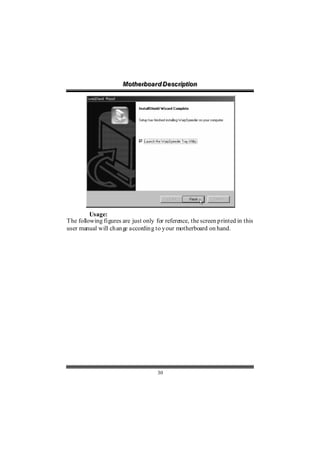
1. Execute the setup execution file, and then the followin g dialo g
will pop up . Please click “Next” button and follow the default
p rocedure to install.
2. When y ou see the following d ialo g in setup p rocedure, it means
setup is completed. If the “Launch the WarpSp eeder Tray
Utility” checkbo x is checked, the Tray Icon utility and
[WarpSp eeder™] utility will be automatically and immediately
launched after y ou click “Finish” button.
29](https://image.slidesharecdn.com/8668d0629cb-130416194731-phpapp02/85/Manual-de-tarjeta-madre-U8668-29-320.jpg)
![Motthe rboa r d D e sc riipttiion
Mo he rboa r d D e sc r p on
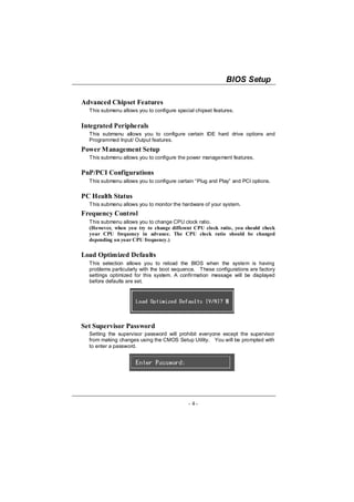
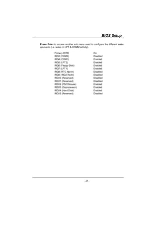
[WarpSpeeder™] includes 1 tray icon and 5 panels:
1. Tray Icon:
Whenever the Tray Icon utility is launched, it will display a
little tray icon on the right side of Windows Taskbar.
This utility is resp onsible for conveniently invoking
[Warp Speeder™] Utility. You can use the mouse by clickin g
the left button in order to invoke [WarpSp eeder™] directly
from the little tray icon or y ou can right-click the little tray
icon to pop up a p op up menu as followin g figure. The
“Launch Utility ” item in the p op up menu has the same
function as mouse left-click on tray icon and “Exit” item
will close Tray Icon utility if selected.
2. Main Panel
If y ou click the tray icon, [WarpSp eeder™] utility will be
invoked. Please refer to the followin g figure; the utility ’s
first window y ou will see is M ain Panel.
Main Panel contains fe ature s as follows:
a. Disp lay the CPU Sp eed, CPU external clo ck, M emory clock,
AGP clock, and PCI clock information.
b. Contains About, V oltage, Overclock, and Hardware M onitor
Buttons for invoking resp ective p anels.
c. With a user-friendly Status Animation, it can rep resent 3
31](https://image.slidesharecdn.com/8668d0629cb-130416194731-phpapp02/85/Manual-de-tarjeta-madre-U8668-31-320.jpg)
![Motthe rboa r d D e sc riipttiion
Mo he rboa r d D e sc r p on
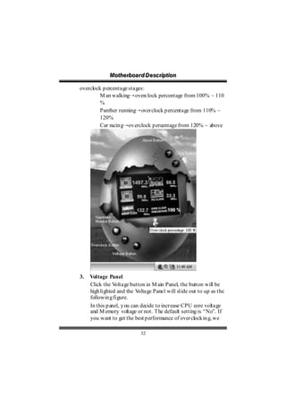
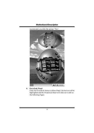
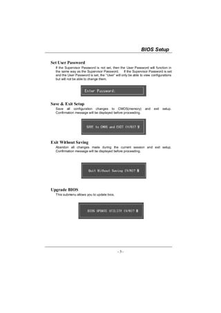
O ve rclock Panel contains the these features:
a. “–3MHz button”, “-1M Hz button”, “+1MHz button”, and
“+3MHz button”: p rovide user the ability to do real-time
overclock adjustment.
Warning:
Manually overclock is potentially dangerous, especially when the overclocking
percentage is over 110 %. We strongly recom mend you verify every speed you
overclock by c lick the Verify button. Or, you can just click Auto overclock button
and let [WarpS peeder™ ] automatically gets the best result for you.
b. “Recovery Dialog button”: Pop up the following d ialo g. Let user
select a restoring way if sy stem need to do a fail-safe reboot.
34](https://image.slidesharecdn.com/8668d0629cb-130416194731-phpapp02/85/Manual-de-tarjeta-madre-U8668-34-320.jpg)
![Motthe rboa r d D e sc riipttiion
Mo he rboa r d D e sc r p on
d. “Auto-overclock button”: User can click this button and
[Warp Sp eeder™] will set the best and stable p erformance
and frequency automatically. [Warp Speeder™] utility will
execute a series of testing until sy stem fail. Then system
will do fail-safe reboot by using Watchdo g function. After
reboot, the [Warp Sp eeder™] utility will restore to the
hardware default setting or load the verified best and stable
frequency accordin g to the Recovery Dialo g’s setting.
e. “Verify button”: User can click this button and
[Warp Sp eeder™] will p roceed a testing for current
frequency. If the testing is ok, then the current frequency
will be saved into system registry. If the testing fail,
system will do a fail-safe rebootin g. After reboot, the
[Warp Sp eeder™] utility will restore to the hardware
default setting or load the verified best and stable
frequency accordin g to the Recovery Dialo g’s setting.
Note:
Because the testing programs, invoked in Auto-overclock and Verify, include
DirectDraw, Direct3D and DirectShow tests, the DirectX 8.1 or newer runtime
library is required. And please make sure your display card’s color depth is
High color (16 bit) or True color( 24/32 bit ) that is required for Direct3D
rendering.
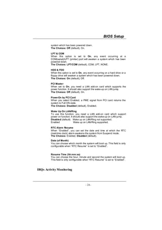
5. Hardware Monitor Panel
Click the Hardware M onitor button in Main Panel, the
button will be highlighted and the Hardware Monitor p anel
will slide out to left as the following figure.
In this p anel, y ou can get the real-time status information of
your system. The information will be refreshed ev ery 1
second.
35](https://image.slidesharecdn.com/8668d0629cb-130416194731-phpapp02/85/Manual-de-tarjeta-madre-U8668-35-320.jpg)
![Motthe rboa r d D e sc riipttiion
Mo he rboa r d D e sc r p on
6. About Panel
Click the “about” button in M ain Panel, the button will be
high lighted and the About Panel will slide out to up as the
followin g figure.
In this p anel, y ou can get model name and detail
information in hints of all the chip set that are related to
overclockin g. You can also get the mainboard ’s BIOS model
and the V ersion number of [Warp Sp eeder™] utility.
36](https://image.slidesharecdn.com/8668d0629cb-130416194731-phpapp02/85/Manual-de-tarjeta-madre-U8668-36-320.jpg)
![Motthe rboa r d D e sc riipttiion
Mo he rboa r d D e sc r p on
Note:
Because the overclock, overvo ltage, and hardware monitor
features are controlled by several separate chip set,
[WarpSp eeder™] divide these features to sep arate panels. If one
chip set is not on board, the correlative button in M ain p anel will
be disabled, but will not interfere other p anels’ functions. This
p rop erty can make [Warp Sp eeder™] utility more robust.
37](https://image.slidesharecdn.com/8668d0629cb-130416194731-phpapp02/85/Manual-de-tarjeta-madre-U8668-37-320.jpg)

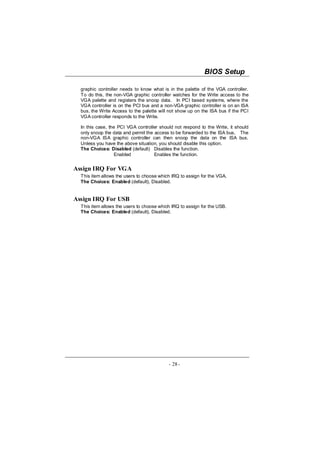

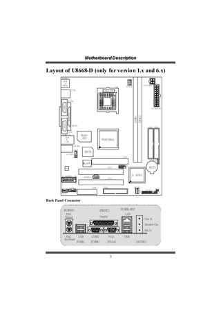
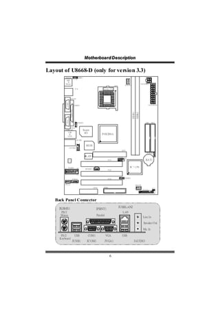
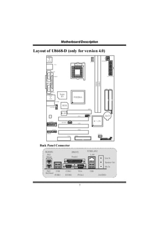
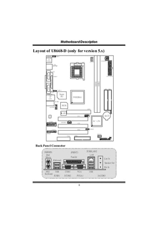
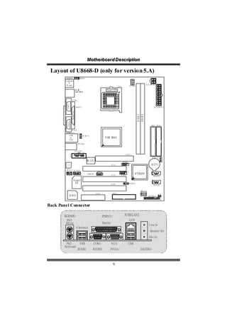
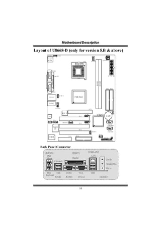
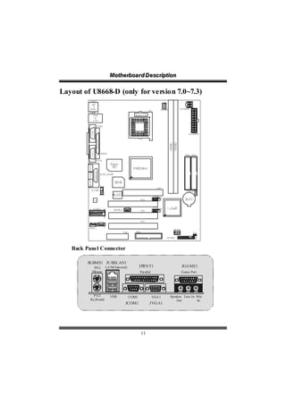
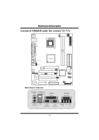
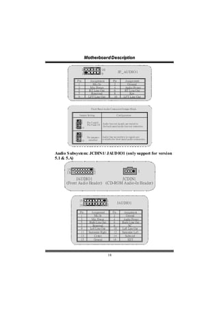
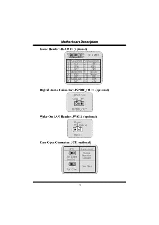
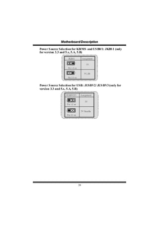
This document provides information about the U8668-D motherboard, including its features, package contents, and layout. It supports Intel Pentium 4 and Celeron D CPUs, up to 2GB of DDR RAM, integrated audio and LAN, and expansion slots including AGP and PCI. The layout sections describe the placement of ports, connectors, and components on the motherboard for different firmware versions.


