Downloaded 41 times
![1-1
[CONTENTS]
SECTION 1. GENERAL
• SERVICING PRECAUTIONS. . . . . . . . . . . . . . . . . . . . . . . . . . . . . . . . . . . . . . . . . . . . . . . . . 1-2
• ESD PRECAUTIONS . . . . . . . . . . . . . . . . . . . . . . . . . . . . . . . . . . . . . . . . . . . . . . . . . . . . . . . 1-4
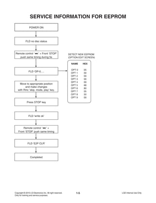
• SERVICE INFORMATION FOR EEPROM . . . . . . . . . . . . . . . . . . . . . . . . . . . . . . . . . . . . . . 1-5
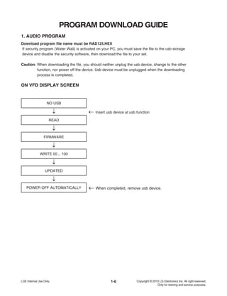
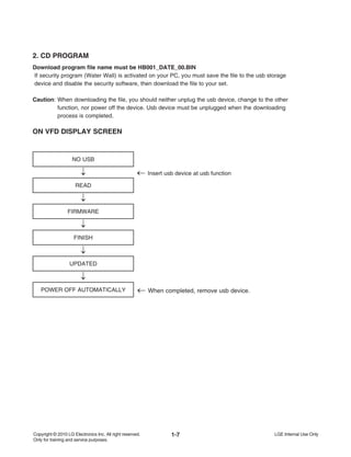
• PROGRAM DOWNLOAD GUIDE. . . . . . . . . . . . . . . . . . . . . . . . . . . . . . . . . . . . . . . . . . . . . . . . . . . . . . . . . . . 1-6
• SPECIFICATIONS . . . . . . . . . . . . . . . . . . . . . . . . . . . . . . . . . . . . . . . . . . . . . . . . . . . . . . . . . 1-8
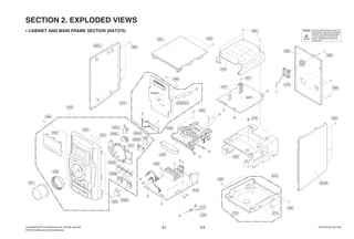
SECTION 2. EXPLODED VIEWS . . . . . . . . . . . . . . . . . . . . . . . . . . . . . . . . . . . . . . . . . . . . . 2-1
• CABINET AND MAIN FRAME SECTION. . . . . . . . . . . . . . . . . . . . . . . . . . . . . . . . . . . . . . . . 2-1
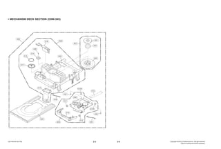
• MECHANISM DECK SECTION (CDM-345). . . . . . . . . . . . . . . . . . . . . . . . . . . . . . . . . . . . . . 2-3
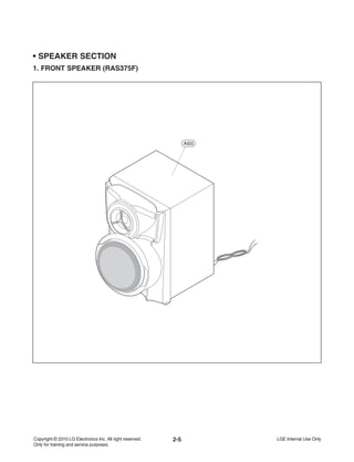
• SPEAKER SECTION . . . . . . . . . . . . . . . . . . . . . . . . . . . . . . . . . . . . . . . . . . . . . . . . . . . . . . . 2-5
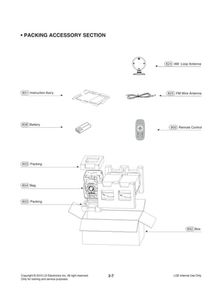
• PACKING ACCESSORY SECTION. . . . . . . . . . . . . . . . . . . . . . . . . . . . . . . . . . . . . . . . . . . . 2-7
SECTION 3. ELECTRICAL PART
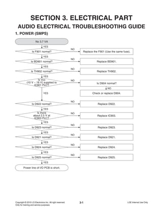
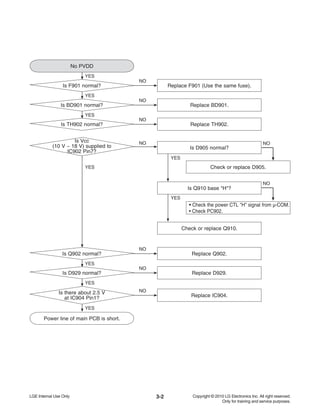
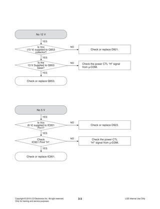
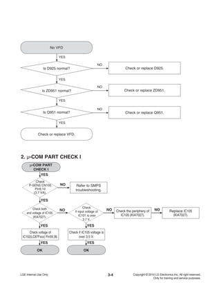
• TROUBLESHOOTING GUIDE . . . . . . . . . . . . . . . . . . . . . . . . . . . . . . . . . . . . . . . . . . . . . . . . 3-1
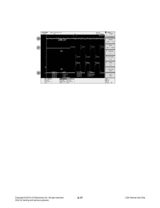
• DETAILS AND WAVEFORMS ON SYSTEM TEST AND DEBUGGING. . . . . . . . . . . . . . . 3-14
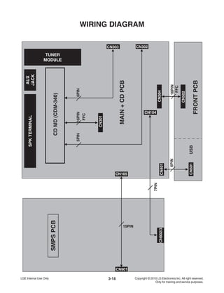
• WIRING DIAGRAM . . . . . . . . . . . . . . . . . . . . . . . . . . . . . . . . . . . . . . . . . . . . . . . . . . . . . . . 3-18
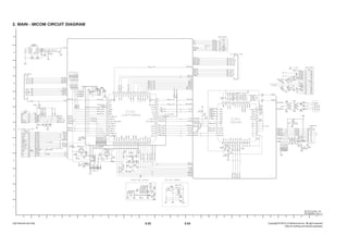
• BLOCK DIAGRAMS . . . . . . . . . . . . . . . . . . . . . . . . . . . . . . . . . . . . . . . . . . . . . . . . . . . . . . 3-19
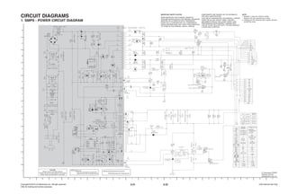
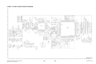
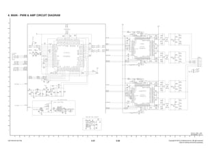
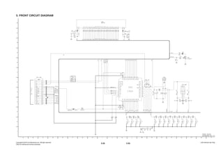
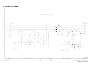
• CIRCUIT DIAGRAMS. . . . . . . . . . . . . . . . . . . . . . . . . . . . . . . . . . . . . . . . . . . . . . . . . . . . . . 3-21
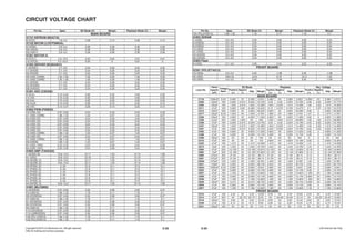
• CIRCUIT VOLTAGE CHART . . . . . . . . . . . . . . . . . . . . . . . . . . . . . . . . . . . . . . . . . . . . . . . . 3-33
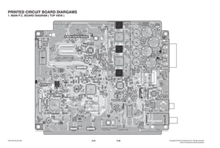
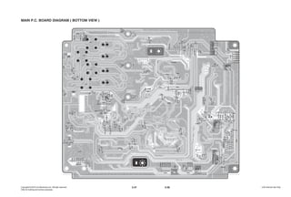
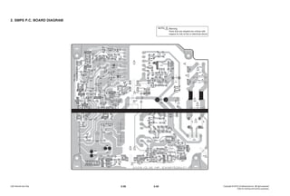
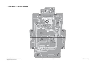
• PRINTED CIRCUIT DIARGAMS . . . . . . . . . . . . . . . . . . . . . . . . . . . . . . . . . . . . . . . . . . . . . 3-35
SECTION 4. REPLACEMENT PARTS LIST . . . . . . . . . . . . . . . . . . . . . . . . . . . . . . . . . . . 4-1](https://image.slidesharecdn.com/lg-rat375b-141222222237-conversion-gate02/85/LG-RAT375B-2-320.jpg)
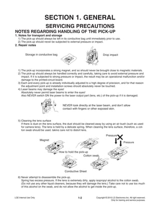
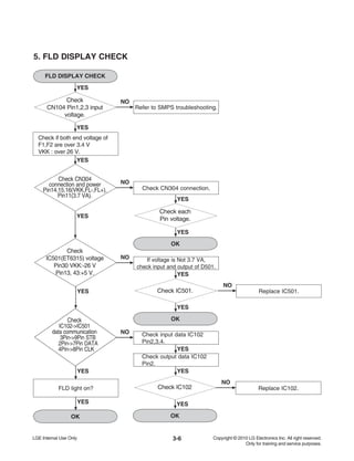
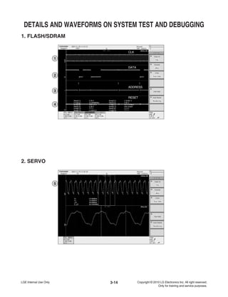
![1-8
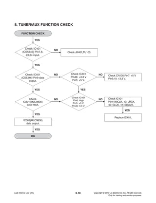
SPECIFICATIONS
• GENERAL
Power supply Refer to main label
Power consumption 60 W
Net Weight 3.5 kg
External dimensions (W x H x D) 202 x 307 x 278 mm
Bus Power Supply (USB) DC 5 V 500 mA
Operating conditions Temperature 5 °C ~ 35 °C,
Operation status: Horizontal
Operating humidity 5 % ~ 85 %
Laser Semiconductor laser, wavelength 650 nm
• TUNER FM/AM [MW]
FM Tuning Range (87.5 ~ 108.0) MHz or (87.50 ~ 108.00) MHz
FM Intermediate Frequency 128 kHz
AM Tuning Range (522 ~ 1 620) kHz, (520 ~ 1 710) kHz or
(522 ~ 1 710) kHz
AM Intermediate Frequency 45 kHz
• AMPLIFIER
Output Power Front : 110 W + 110 W (4 Ω at 1 kHz, THD 10 %)
Sub Woofer : 150 W (3 Ω at 60 Hz, THD 10 %)
• CD
Frequency Response (40 ~ 20 000) Hz
Signal-to-noise ratio 75 dB
Dynamic range 80 dB
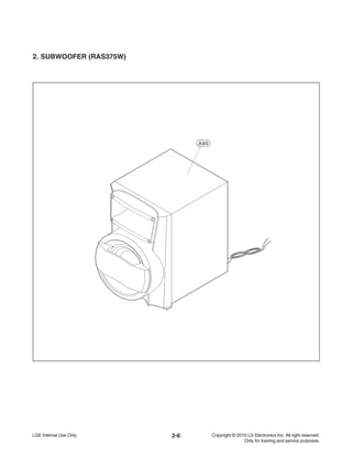
• SPEAKERS
Front Speaker Sub Woofer
Type 2 Way 2 Speaker 1 Way 1 Speaker
Impedance 4 Ω 3 Ω
Rated Input Power 110 W 150 W
Max. Input Power 220 W 300 W
Net Dimensions (W x H x D) 232 x 346 x 289 mm 250 x 346 x 356 mm
Net Weight 3.3 kg 5.5 kg
Designs and specifications are subject to change without prior notice](https://image.slidesharecdn.com/lg-rat375b-141222222237-conversion-gate02/85/LG-RAT375B-9-320.jpg)

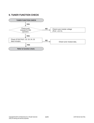
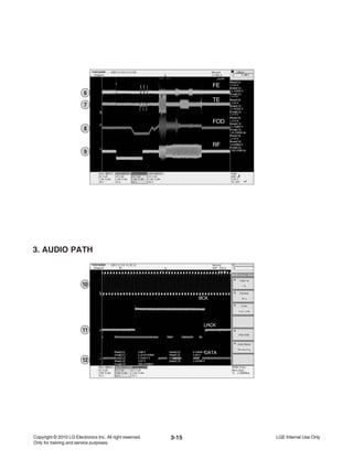
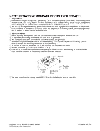
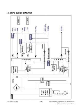
![3-19
BLOCK DIAGRAMS
1. MAIN BLOCK DIAGRAM
P/UP
M
A,B,C,D,E,F
PD
LD
CD_DIN_DOUT
CD_MCK/CD_R/W
BUSY;CD-16M SUBSYQ;
9543-RST;
VFD
AMP
TAS5612
DMA[0..11],DB[0..15
]
DSCK#,CKE,CS0#,RAS0
#
TDO
SLDO
SPDO
FDO
12MHZ
16.93MHZ
POWER
I/F
3.7V
12V
DAT, CLK, RST, CE, INT
RST, WEN#,CE#
A[0.. 18], DB[0..15]
OP/CL
OP/CLLI
MIT
CD-BCK/LRCK/DOUTA
DAC-MCLK
P-SENSE
PWM
PS9850
DO
STB
CLK
ADC-CLK
ADC-DAT
ADC-RST
ADC-DATA
R/L
R/L
I2SCLK
DAC-BCK/LRCK/MCLK
DAC-DATA
PWM-RST
PWM-CLK
PWM-DAT
PDN
SD; OTW
FL+
FL-
FR+
FR-
D+/-
P-CTRL
R
L
DAT
CLK
SPI-DO/DI/CLK/CS
RMCKEY
9.8304MH
Z
32.766khz
NewPWM
SWSW+
SW-](https://image.slidesharecdn.com/lg-rat375b-141222222237-conversion-gate02/85/LG-RAT375B-34-320.jpg)

The document is a service manual for an LG Mini Hi-Fi System model RAT375. It contains sections on safety precautions for servicing the unit, ESD precautions, specifications for the unit, exploded views of parts, and electrical diagrams. The manual provides guidance on servicing the unit safely and properly as well as replacing parts. It aims to prevent damage from electrostatic discharge or other hazards during repair.


