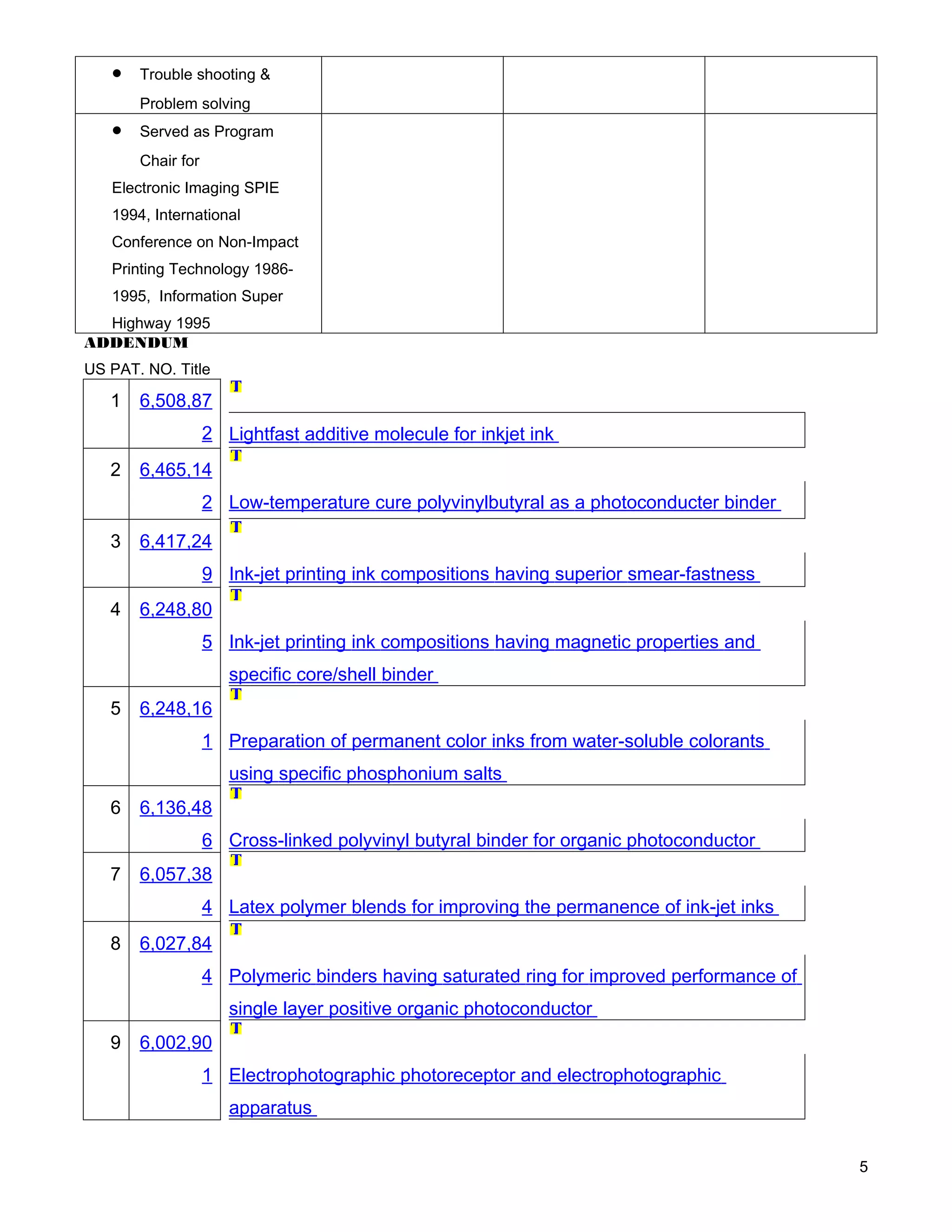
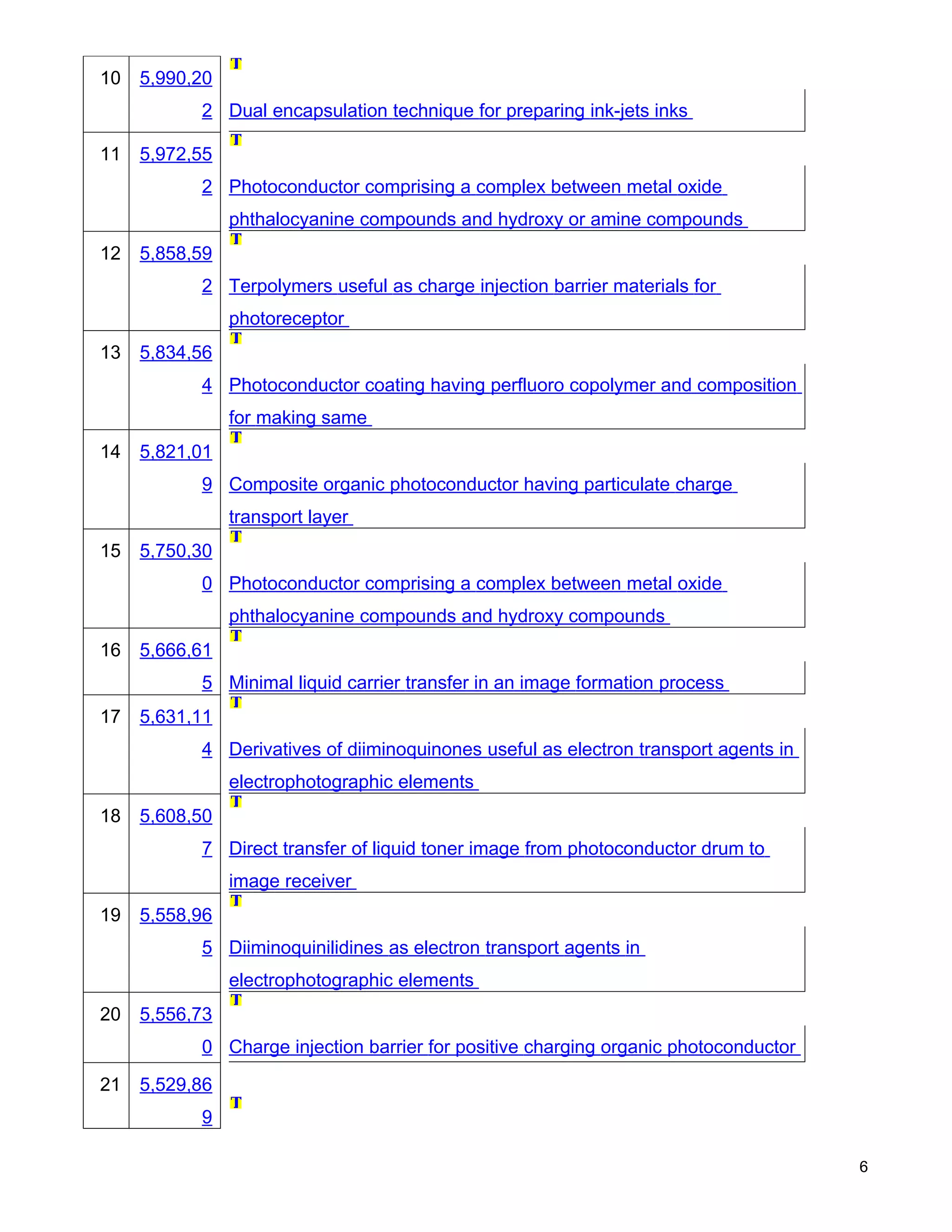
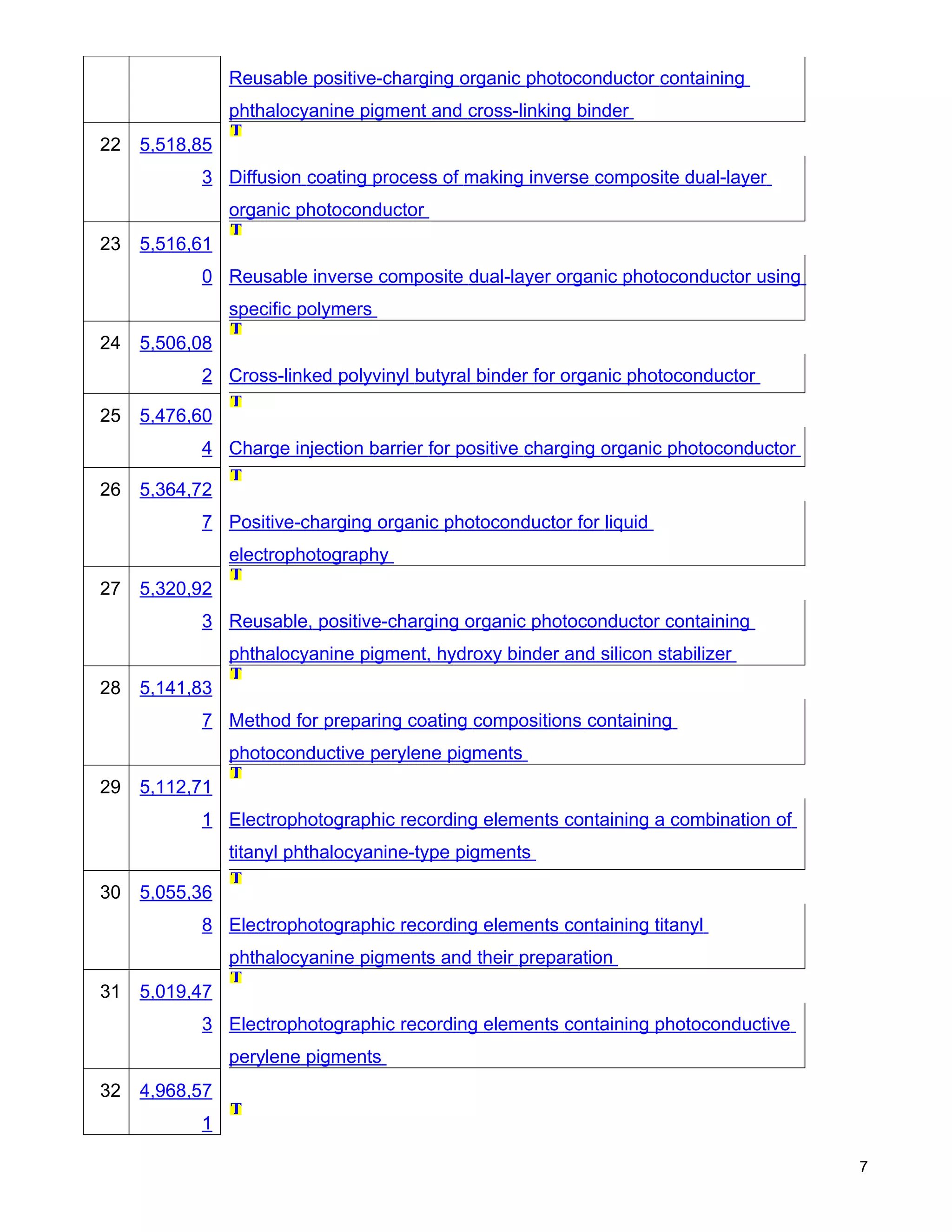
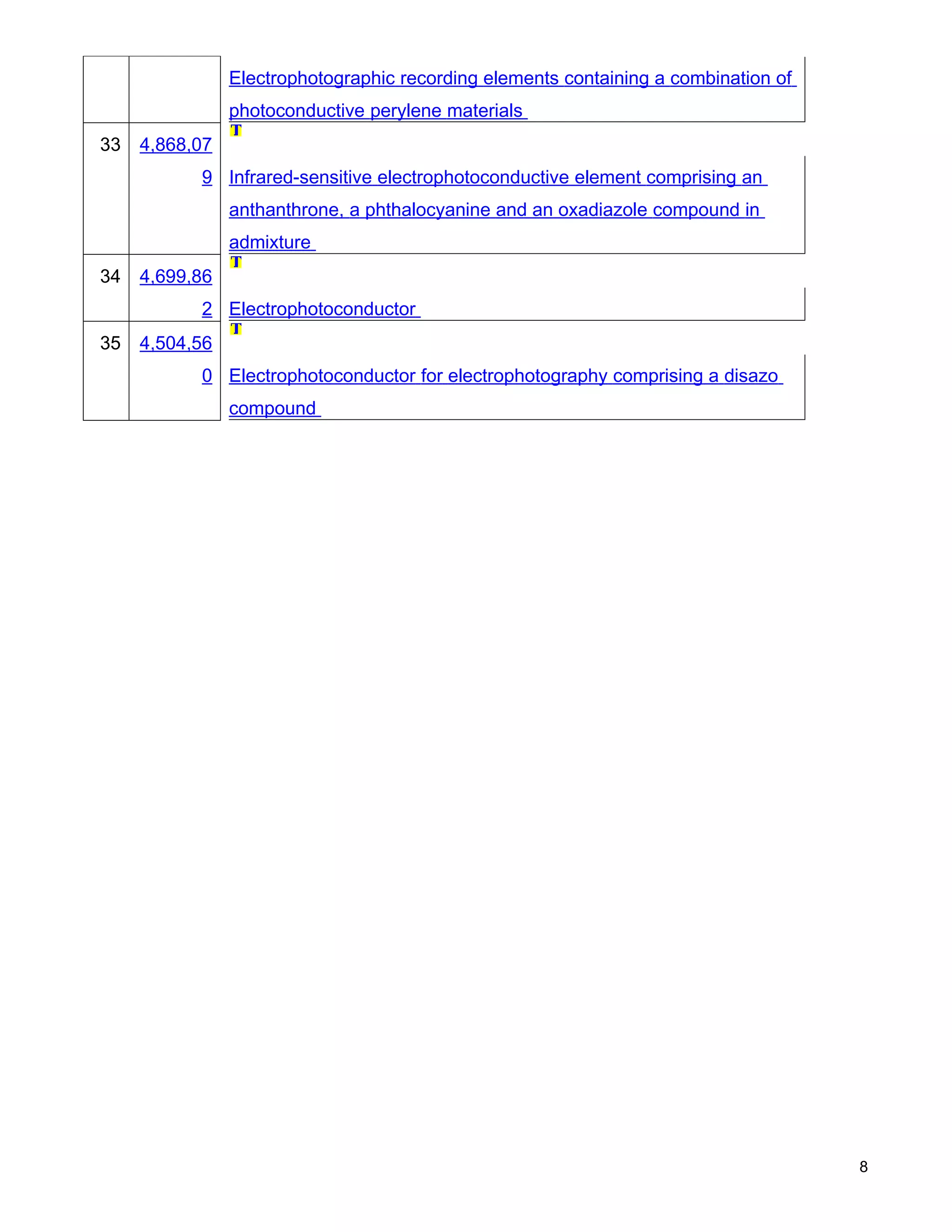
Dr. KHE NGUYEN
                       SAIGON HI TECH PARK RESEARCH LABORATORIES
        LOT I3 N2 STREET, SAIGON HITECH PARK, DISTRICT 9, HOCHIMINH CITY, VIET NAM

                                                          Email Kng3328196@aol.com

____________________________________________________________________________________


                     NANOTECHNOLOGY & CLEAN TECH SCIENTIST
         ____________________________________________________________________________________


                                                 SUMMARY

        Over 29 years proven background of interdisciplinary integration into novel concepts, process &
material & product development, technical leader /scientist with 36 US Patents
        Experience includes nanotechnology materials including carbon nano tube, graphene hybrid composite, ,
renewable energy including fuel cell technology, semiconductor sensor products (MEMS applications) , wafer
level packaging(WLCSP) process , ink jet ink technology & product development , organic photoconductor (OPC)
and organic LED (OLED) materials , polymer chemistry & physics, water base chemistry , colorant chemistry,
material analysis and technical project management . Excellent analytical and organizational skills with a focus to
detail . Strong communication skills with an ability to work well with all levels of management and personnel.
Dependable and reliable worker who meets deadlines and is committed to quality work.


                                               EXPERIENCE
SAIGON HI TECH PARK RESEARCH LABORATORIES, People Committee of Ho Chi Minh City,
Ho Chi Minh City, Vietnam
                                                    2009-present

VICE LAB DIRECTOR
    •   Developed Water Power Generator
    •   Developed Graphene Hybrid Composite
   • Developed “Liquid” Nano Coal for Low cost Fuel Cell
SAIGON HI TECH PARK RESEARCH LABORATORIES, People Committee of Ho Chi Minh City,
Ho Chi Minh City, Vietnam
                                                         2002-2009
LAB DIRECTOR
    •   Organized central laboratories of Saigon Hi Tech Park, comprised of 4 major laboratories : a) wafer fab
        for R&D and production of microelectronics including chip, MEMS chip b) Advanced material lab c)
        BioMEMS lab d) Metrology lab
    •   Proposed and got funded 11.5 millions USD to establish SHTP Labs


  • Advisory member for National University System in Ho Chi Minh City, Vietnam
MEASUREMENT SPECIALTIES, IC SENSOR DIV, MILPITAS,CA                             2000-2002


                                                                                                                  1
Research Scientist,
MEMS device processing including
        •   novel carbon materials for CD & side wall control
        •   polymer chemistry & physics for bonding process in mirror array,accelerometer, actuator
        •   Integration process of benzocyclobuten (BCB) for complex CMOS platform
        •   Masking materials for special toolings of SOI wafer : deep RIE, deep trench photolithography ,high resolution
            masking (<1um) and stepper
        •   Dry film resist on various substrates (Si, glass, sapphire, . . .) and double side etch process
        •   Interdisciplinary innovation of process development for yield improvement
        •   Deep experiences and special skills on wide variety of organic materials : humidity sensing
            polyimide, photoimageable polyimides and siloxane based polymers, low K polymer network , thick
            photo resist modules
        •   Developed robust solutions for adhesion/de-adhesion/stripping issues in small cavities and special
            surfaces
        •   Developed novel Si wet etch process
        •   Wet & dry etch process for metals, oxides, nitrides


APTOS CORPORATION, MILPITAS, CA                                                                             1999-2000

Principle Process Development Engineer
        •   Responsible for WLCSP (Wafer Level Chip Scale Packaging) , focused on bumping (Cu, solder, Au,
            lead free bump, . .) product development
        •   Process integration
                           a)       Novel wet etch process of polyimide (PI) (patent application pending)
                           b)       Low K material process module
                           c)       thick photo-resist module for electroplating
                           d)       Redistribution layer process module
                           e)       Trouble shooting for integration technology
                           f)       Responsible for bump inspection criteria: bump shape,CD, bump height,
                                chemical component, shear strength, reflow characteristics . . .

HEWLETT-PACKARD LABS, PALO ALTO, CA                                                                       1992 - 1999

Principle Scientist
Built computer peripheral technologies & printer products including
        •   ink chemistry for inkjet printer
        •   photoconductor chemistry & manufacturing process for laser printer
        •   organic light emitting diode (OLED)
        •   leading technical team in technology building, transferring , product development and market
            introduction
        •   tailoring the chemistry to meet new applications in imaging hardware products
                                                                                                                        2
RICOH CORPORATION OF AMERICA, SAN JOSE, CA                                                           1989 - 1992

Project Manager
       •   Proposed a business & master plan
       •   Raised US$2M funding for organic photoconductor (OPC) dedicated for desk top laser printer
           product
       •   Managed the OPC     project team including building of new facilities for coating, hiring staff,
           organizing & managing technical team,
       •   Demonstrated product prototype in a short period of time


EASTMAN KODAK RESEARCH LABS, ROCHESTER, NY                                                           1985 - 1989

Senior Scientist
       •   Researched and developed organic photoconductor (OPC) for high speed color copier & laser
           printer

DAINIPPON INK & CHEMICALS , TOKYO , JAPAN                                                               1982-
       1985
Senior Scientist
       •   Responsible for the development and market introduction of novel organic photoconductor (OPC) for
           destop copier SFT600

                                               CITIZENSHIP


                                               US Citizenship

                                                EDUCATION


                          PhD, Tokyo Institute of Technology , Tokyo, Japan, 1982
                            (Information Physics/Imaging Science & Technology )

                                               LINGUISTIC SKILLS
                                       Fluent English, Japanese, Vietnamese

                                                      PATENTS
                                   I own 35 US Patents and 30 Japanese Patents


                                                                                                                3
SKILL SET INVENTORY


     KHE NGUYEN                        1808 FARNDON LOS ALTOS ,CA94024
TECHNOLOGY BUILDING & PRODUCT DEVELOPMENT SCIENTIST
ENGINEER/

Summary

PhD scientist involved in IC sensor product development (MEMS applications) , Electronic Packaging (Wafer
Level Packaging , bumping technology), ink jet ink formulation , photosensitive & display materials , polymer
chemistry & physics, water base chemistry , colorant chemistry, material analysis and technical project
management

    Research & Development         Project Management            Product development       Patents &
                                                                                           Innovation
    •   Wafer Level Packaging          •       Project              •   Product                Suggesting novel
    •   Electroplating, bumping                proposal                 qualification          concepts

        technology
    •   IC sensor processing &         •       Fund raising         •   ISO                    Proving working
        fabrication (MEMS)                                                                     concepts
    •   Accelerometer, humidity            •     Staff hiring       •   Customer               Invention
        sensor, micromirror                                             satisfaction           desclosure
        array, gyroscope                                                strategy
        applications
    •   Semiconductor bond             •       Budget               •   Quality control        Patent application
    process & materials                        management
    •   Photoimageable polymer         •       Technical staff      •   Documentation          32US Patent
        process                        management                                              granted
    •   Wet and dry etch               •       Project              •   Product                36 Japanese
        process of polymers &                  milestone                introduction           Patents Granted
        silicon                        time table
    •   Water based & salt &           •       Technical            •   Design of
        colorant chemistry                     project                  Experiments
                                       management
    •   Tailoring chemicals
    •   Emulsion polymers
    •   Photosensitive materials
        & Organic LED devices
    •   Electrophotographic
        materials


                                                                                                                 4
•   Trouble shooting &
       Problem solving
   •   Served as Program
       Chair for
   Electronic Imaging SPIE
   1994, International
   Conference on Non-Impact
   Printing Technology 1986-
   1995, Information Super
  Highway 1995
ADDENDUM
US PAT. NO. Title

   1   6,508,87
                   2 Lightfast additive molecule for inkjet ink
   2   6,465,14
                   2 Low-temperature cure polyvinylbutyral as a photoconducter binder

   3   6,417,24
                   9 Ink-jet printing ink compositions having superior smear-fastness
   4   6,248,80
                   5 Ink-jet printing ink compositions having magnetic properties and
                      specific core/shell binder
   5   6,248,16
                   1 Preparation of permanent color inks from water-soluble colorants
                      using specific phosphonium salts
   6   6,136,48
                   6 Cross-linked polyvinyl butyral binder for organic photoconductor
   7   6,057,38
                   4 Latex polymer blends for improving the permanence of ink-jet inks
   8   6,027,84
                   4 Polymeric binders having saturated ring for improved performance of
                      single layer positive organic photoconductor
   9   6,002,90
                   1 Electrophotographic photoreceptor and electrophotographic
                      apparatus


                                                                                           5
10   5,990,20
           2 Dual encapsulation technique for preparing ink-jets inks

11   5,972,55
           2 Photoconductor comprising a complex between metal oxide
                phthalocyanine compounds and hydroxy or amine compounds
12   5,858,59
           2 Terpolymers useful as charge injection barrier materials for
                photoreceptor
13   5,834,56
           4 Photoconductor coating having perfluoro copolymer and composition
                for making same
14   5,821,01
           9 Composite organic photoconductor having particulate charge
                transport layer
15   5,750,30
           0 Photoconductor comprising a complex between metal oxide
                phthalocyanine compounds and hydroxy compounds
16   5,666,61
           5 Minimal liquid carrier transfer in an image formation process
17   5,631,11
           4 Derivatives of diiminoquinones useful as electron transport agents in
                electrophotographic elements
18   5,608,50
           7 Direct transfer of liquid toner image from photoconductor drum to
                image receiver
19   5,558,96
           5 Diiminoquinilidines as electron transport agents in
                electrophotographic elements
20   5,556,73
           0 Charge injection barrier for positive charging organic photoconductor

21   5,529,86
           9

                                                                                     6
Reusable positive-charging organic photoconductor containing
                phthalocyanine pigment and cross-linking binder
22   5,518,85
           3 Diffusion coating process of making inverse composite dual-layer
                organic photoconductor
23   5,516,61
           0 Reusable inverse composite dual-layer organic photoconductor using
                specific polymers
24   5,506,08
           2 Cross-linked polyvinyl butyral binder for organic photoconductor

25   5,476,60
           4 Charge injection barrier for positive charging organic photoconductor

26   5,364,72
           7 Positive-charging organic photoconductor for liquid
                electrophotography
27   5,320,92
           3 Reusable, positive-charging organic photoconductor containing
                phthalocyanine pigment, hydroxy binder and silicon stabilizer
28   5,141,83
           7 Method for preparing coating compositions containing
                photoconductive perylene pigments
29   5,112,71
           1 Electrophotographic recording elements containing a combination of
                titanyl phthalocyanine-type pigments

30   5,055,36
           8 Electrophotographic recording elements containing titanyl
                phthalocyanine pigments and their preparation
31   5,019,47
           3 Electrophotographic recording elements containing photoconductive
                perylene pigments
32   4,968,57
           1

                                                                                     7
Electrophotographic recording elements containing a combination of
                photoconductive perylene materials
33   4,868,07
           9 Infrared-sensitive electrophotoconductive element comprising an
                anthanthrone, a phthalocyanine and an oxadiazole compound in
                admixture
34   4,699,86
           2 Electrophotoconductor
35   4,504,56
           0 Electrophotoconductor for electrophotography comprising a disazo
                compound


                                                                                     8

KTubeTech.com-Danh-sach-bang-phat-minh

  • 1.
    Dr. KHE NGUYEN SAIGON HI TECH PARK RESEARCH LABORATORIES LOT I3 N2 STREET, SAIGON HITECH PARK, DISTRICT 9, HOCHIMINH CITY, VIET NAM Email Kng3328196@aol.com ____________________________________________________________________________________ NANOTECHNOLOGY & CLEAN TECH SCIENTIST ____________________________________________________________________________________ SUMMARY Over 29 years proven background of interdisciplinary integration into novel concepts, process & material & product development, technical leader /scientist with 36 US Patents Experience includes nanotechnology materials including carbon nano tube, graphene hybrid composite, , renewable energy including fuel cell technology, semiconductor sensor products (MEMS applications) , wafer level packaging(WLCSP) process , ink jet ink technology & product development , organic photoconductor (OPC) and organic LED (OLED) materials , polymer chemistry & physics, water base chemistry , colorant chemistry, material analysis and technical project management . Excellent analytical and organizational skills with a focus to detail . Strong communication skills with an ability to work well with all levels of management and personnel. Dependable and reliable worker who meets deadlines and is committed to quality work. EXPERIENCE SAIGON HI TECH PARK RESEARCH LABORATORIES, People Committee of Ho Chi Minh City, Ho Chi Minh City, Vietnam 2009-present VICE LAB DIRECTOR • Developed Water Power Generator • Developed Graphene Hybrid Composite • Developed “Liquid” Nano Coal for Low cost Fuel Cell SAIGON HI TECH PARK RESEARCH LABORATORIES, People Committee of Ho Chi Minh City, Ho Chi Minh City, Vietnam 2002-2009 LAB DIRECTOR • Organized central laboratories of Saigon Hi Tech Park, comprised of 4 major laboratories : a) wafer fab for R&D and production of microelectronics including chip, MEMS chip b) Advanced material lab c) BioMEMS lab d) Metrology lab • Proposed and got funded 11.5 millions USD to establish SHTP Labs • Advisory member for National University System in Ho Chi Minh City, Vietnam MEASUREMENT SPECIALTIES, IC SENSOR DIV, MILPITAS,CA 2000-2002 1
  • 2.
    Research Scientist, MEMS deviceprocessing including • novel carbon materials for CD & side wall control • polymer chemistry & physics for bonding process in mirror array,accelerometer, actuator • Integration process of benzocyclobuten (BCB) for complex CMOS platform • Masking materials for special toolings of SOI wafer : deep RIE, deep trench photolithography ,high resolution masking (<1um) and stepper • Dry film resist on various substrates (Si, glass, sapphire, . . .) and double side etch process • Interdisciplinary innovation of process development for yield improvement • Deep experiences and special skills on wide variety of organic materials : humidity sensing polyimide, photoimageable polyimides and siloxane based polymers, low K polymer network , thick photo resist modules • Developed robust solutions for adhesion/de-adhesion/stripping issues in small cavities and special surfaces • Developed novel Si wet etch process • Wet & dry etch process for metals, oxides, nitrides APTOS CORPORATION, MILPITAS, CA 1999-2000 Principle Process Development Engineer • Responsible for WLCSP (Wafer Level Chip Scale Packaging) , focused on bumping (Cu, solder, Au, lead free bump, . .) product development • Process integration a) Novel wet etch process of polyimide (PI) (patent application pending) b) Low K material process module c) thick photo-resist module for electroplating d) Redistribution layer process module e) Trouble shooting for integration technology f) Responsible for bump inspection criteria: bump shape,CD, bump height, chemical component, shear strength, reflow characteristics . . . HEWLETT-PACKARD LABS, PALO ALTO, CA 1992 - 1999 Principle Scientist Built computer peripheral technologies & printer products including • ink chemistry for inkjet printer • photoconductor chemistry & manufacturing process for laser printer • organic light emitting diode (OLED) • leading technical team in technology building, transferring , product development and market introduction • tailoring the chemistry to meet new applications in imaging hardware products 2
  • 3.
    RICOH CORPORATION OFAMERICA, SAN JOSE, CA 1989 - 1992 Project Manager • Proposed a business & master plan • Raised US$2M funding for organic photoconductor (OPC) dedicated for desk top laser printer product • Managed the OPC project team including building of new facilities for coating, hiring staff, organizing & managing technical team, • Demonstrated product prototype in a short period of time EASTMAN KODAK RESEARCH LABS, ROCHESTER, NY 1985 - 1989 Senior Scientist • Researched and developed organic photoconductor (OPC) for high speed color copier & laser printer DAINIPPON INK & CHEMICALS , TOKYO , JAPAN 1982- 1985 Senior Scientist • Responsible for the development and market introduction of novel organic photoconductor (OPC) for destop copier SFT600 CITIZENSHIP US Citizenship EDUCATION PhD, Tokyo Institute of Technology , Tokyo, Japan, 1982 (Information Physics/Imaging Science & Technology ) LINGUISTIC SKILLS Fluent English, Japanese, Vietnamese PATENTS I own 35 US Patents and 30 Japanese Patents 3
  • 4.
    SKILL SET INVENTORY KHE NGUYEN 1808 FARNDON LOS ALTOS ,CA94024 TECHNOLOGY BUILDING & PRODUCT DEVELOPMENT SCIENTIST ENGINEER/ Summary PhD scientist involved in IC sensor product development (MEMS applications) , Electronic Packaging (Wafer Level Packaging , bumping technology), ink jet ink formulation , photosensitive & display materials , polymer chemistry & physics, water base chemistry , colorant chemistry, material analysis and technical project management Research & Development Project Management Product development Patents & Innovation • Wafer Level Packaging • Project • Product Suggesting novel • Electroplating, bumping proposal qualification concepts technology • IC sensor processing & • Fund raising • ISO Proving working fabrication (MEMS) concepts • Accelerometer, humidity • Staff hiring • Customer Invention sensor, micromirror satisfaction desclosure array, gyroscope strategy applications • Semiconductor bond • Budget • Quality control Patent application process & materials management • Photoimageable polymer • Technical staff • Documentation 32US Patent process management granted • Wet and dry etch • Project • Product 36 Japanese process of polymers & milestone introduction Patents Granted silicon time table • Water based & salt & • Technical • Design of colorant chemistry project Experiments management • Tailoring chemicals • Emulsion polymers • Photosensitive materials & Organic LED devices • Electrophotographic materials 4
  • 5.
    Trouble shooting & Problem solving • Served as Program Chair for Electronic Imaging SPIE 1994, International Conference on Non-Impact Printing Technology 1986- 1995, Information Super Highway 1995 ADDENDUM US PAT. NO. Title 1 6,508,87 2 Lightfast additive molecule for inkjet ink 2 6,465,14 2 Low-temperature cure polyvinylbutyral as a photoconducter binder 3 6,417,24 9 Ink-jet printing ink compositions having superior smear-fastness 4 6,248,80 5 Ink-jet printing ink compositions having magnetic properties and specific core/shell binder 5 6,248,16 1 Preparation of permanent color inks from water-soluble colorants using specific phosphonium salts 6 6,136,48 6 Cross-linked polyvinyl butyral binder for organic photoconductor 7 6,057,38 4 Latex polymer blends for improving the permanence of ink-jet inks 8 6,027,84 4 Polymeric binders having saturated ring for improved performance of single layer positive organic photoconductor 9 6,002,90 1 Electrophotographic photoreceptor and electrophotographic apparatus 5
  • 6.
    10 5,990,20 2 Dual encapsulation technique for preparing ink-jets inks 11 5,972,55 2 Photoconductor comprising a complex between metal oxide phthalocyanine compounds and hydroxy or amine compounds 12 5,858,59 2 Terpolymers useful as charge injection barrier materials for photoreceptor 13 5,834,56 4 Photoconductor coating having perfluoro copolymer and composition for making same 14 5,821,01 9 Composite organic photoconductor having particulate charge transport layer 15 5,750,30 0 Photoconductor comprising a complex between metal oxide phthalocyanine compounds and hydroxy compounds 16 5,666,61 5 Minimal liquid carrier transfer in an image formation process 17 5,631,11 4 Derivatives of diiminoquinones useful as electron transport agents in electrophotographic elements 18 5,608,50 7 Direct transfer of liquid toner image from photoconductor drum to image receiver 19 5,558,96 5 Diiminoquinilidines as electron transport agents in electrophotographic elements 20 5,556,73 0 Charge injection barrier for positive charging organic photoconductor 21 5,529,86 9 6
  • 7.
    Reusable positive-charging organicphotoconductor containing phthalocyanine pigment and cross-linking binder 22 5,518,85 3 Diffusion coating process of making inverse composite dual-layer organic photoconductor 23 5,516,61 0 Reusable inverse composite dual-layer organic photoconductor using specific polymers 24 5,506,08 2 Cross-linked polyvinyl butyral binder for organic photoconductor 25 5,476,60 4 Charge injection barrier for positive charging organic photoconductor 26 5,364,72 7 Positive-charging organic photoconductor for liquid electrophotography 27 5,320,92 3 Reusable, positive-charging organic photoconductor containing phthalocyanine pigment, hydroxy binder and silicon stabilizer 28 5,141,83 7 Method for preparing coating compositions containing photoconductive perylene pigments 29 5,112,71 1 Electrophotographic recording elements containing a combination of titanyl phthalocyanine-type pigments 30 5,055,36 8 Electrophotographic recording elements containing titanyl phthalocyanine pigments and their preparation 31 5,019,47 3 Electrophotographic recording elements containing photoconductive perylene pigments 32 4,968,57 1 7
  • 8.
    Electrophotographic recording elementscontaining a combination of photoconductive perylene materials 33 4,868,07 9 Infrared-sensitive electrophotoconductive element comprising an anthanthrone, a phthalocyanine and an oxadiazole compound in admixture 34 4,699,86 2 Electrophotoconductor 35 4,504,56 0 Electrophotoconductor for electrophotography comprising a disazo compound 8