This document provides an executive summary of a two-day lecture series on optics-microwave interactions. The first day covered an overview of the field and state-of-the-art, hybrid integration of optoelectronic components, and optoelectronic transducers. Applications presented included fiber-fed radio systems, optical distribution of RF/millimeter-wave signals, and applications to phased arrays. The second day covered optical processing and control of microwave signals, optical networks for radar and electronic warfare, and novel techniques in optical analog-to-digital converters and medical imaging. The material supported lectures held in France, Germany, and Hungary in September 2002 under sponsorship of RTO's Sensors and Electronics Technology Panel.


![I-5
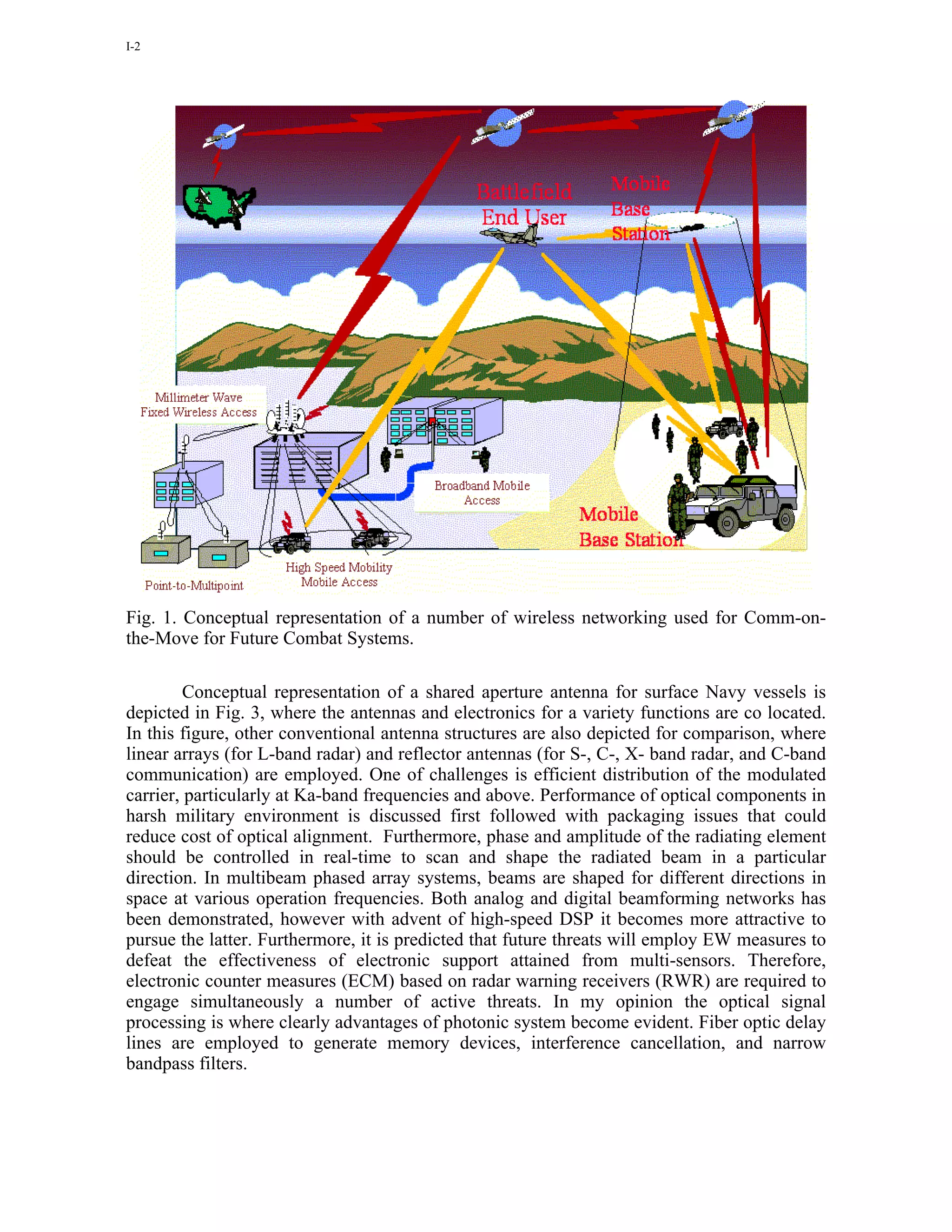
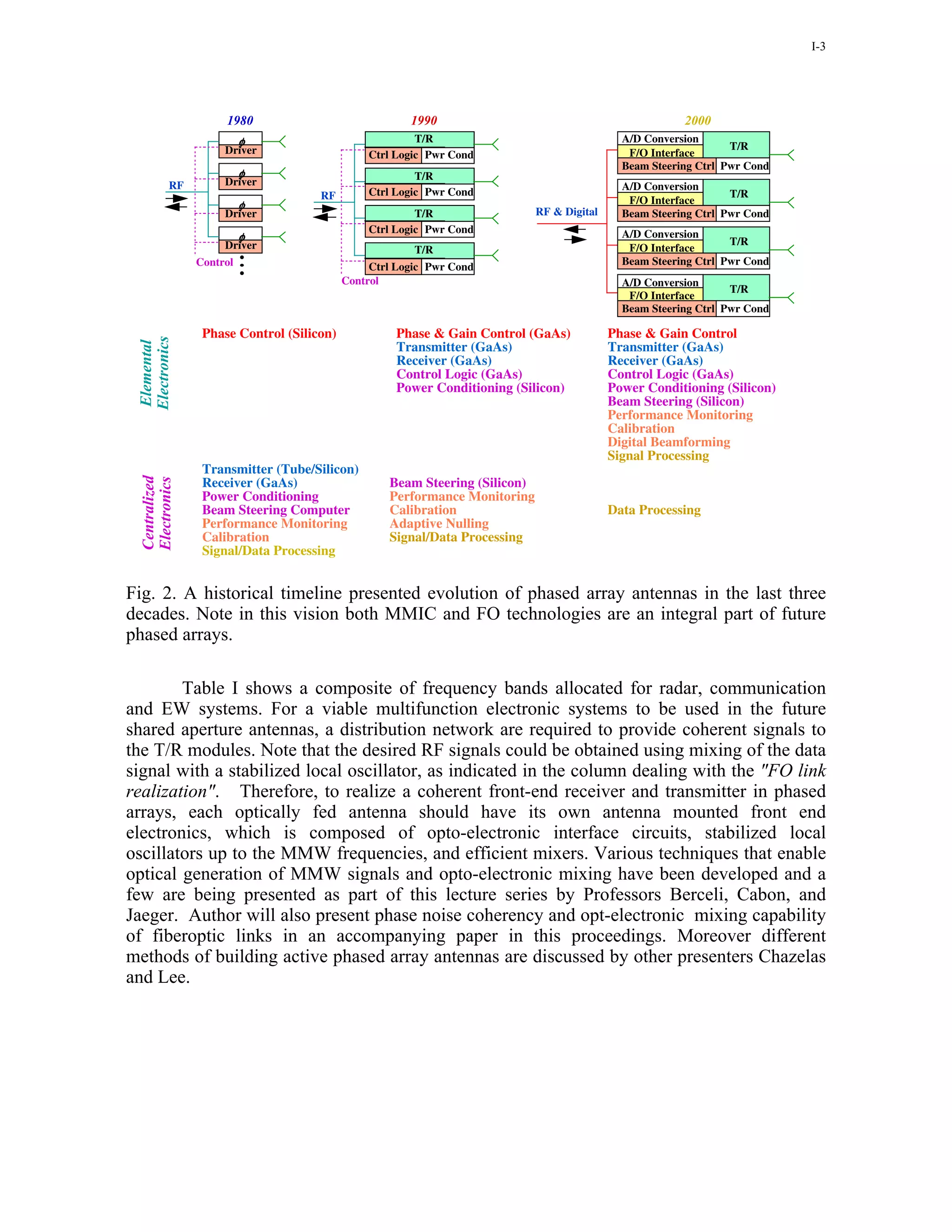
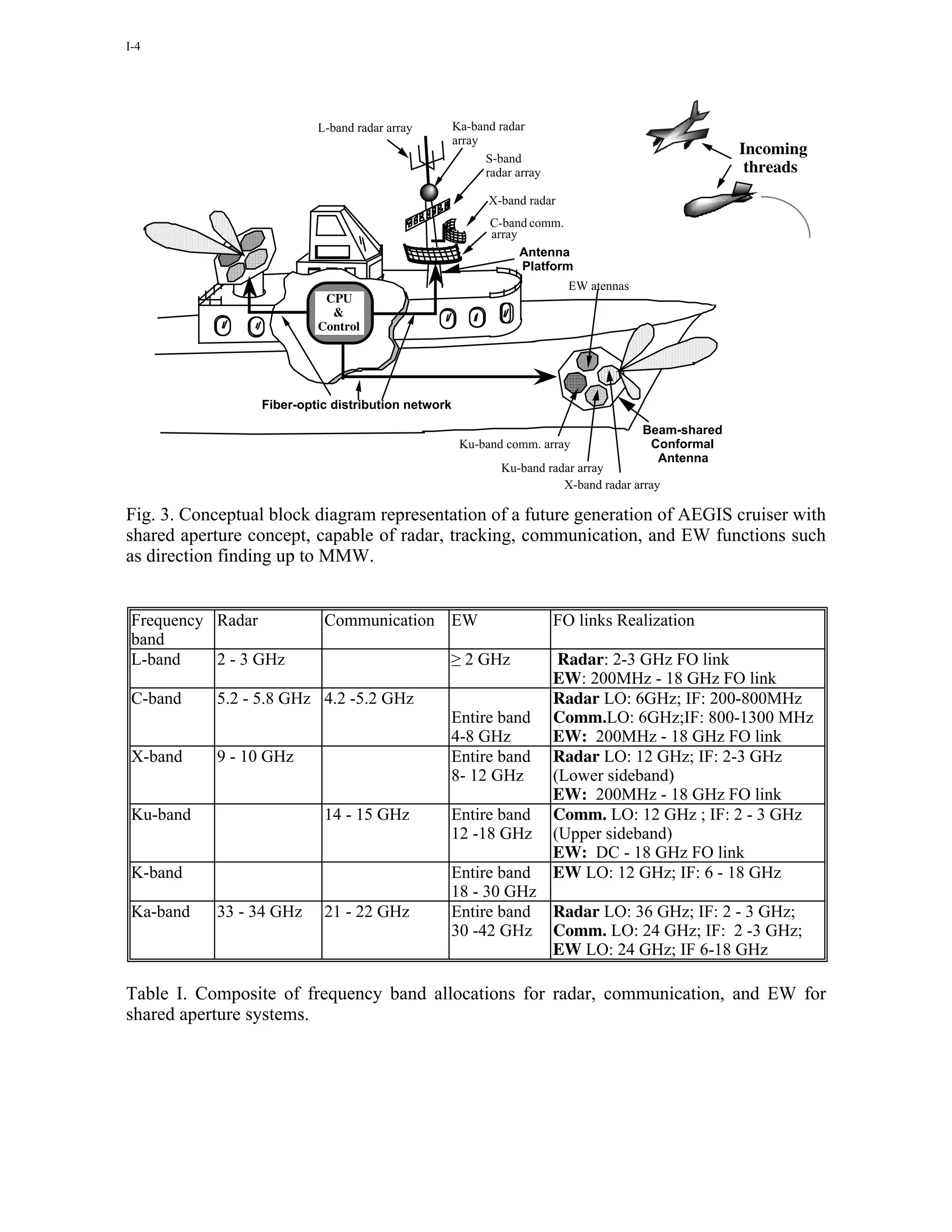
3.0 Fiberoptic Distribution for Phased Array Antennas
One of the simplest methods of providing FO links for antenna remoting is based on
the concept of direct replacement of the electrical interconnects. However, there are
challenges associated with reliability of optical components, cost of system integration, and
the architecture employed for achieving the best attributes possible.
Device Innovations and Reliability: A vast number of research work reported in literature
have focused on the device improvements to meet the performance requirement of
commercial fiber optic communication. Performance of sampled directly and externally
modulated fiber optic links operating at S-band is rendered in Table II, where the best
performance is achieved. For DFB laser monolithically integrated with EA modulator. The
performance of mode-locked laser is quite acceptable (The results of MZ modulator may
appear worse than what is reported in literature, but in this case a semiconductor laser with
optical power of only a few mW is used as a source. Monolithically integrated EA modulator
with sampled grating DBR laser (SGDBR) [1] has been developed where SFDR of 120
dB.Hz2/3 is achieved over a large tuning bandwidth. However, the harsh military environment
impose additional burden on the performance of lightwave technology components.
Directly Modulated Externally Modulated
FO Links FO Links
Mode- Ortel DFB/EA Sumitomo MZ
Loked Laser DFB Laser Modulator Modulator
Frequency 2.2GHz 2.5GHz 2.2GHz 2.5GHz
Gain (dB) -8 -44 -12 -40
IP3 (dBm) +17 +27 +14 +23
Noise Floor -142 -151 -151 -151
(dBm/Hz)
SFDR
101 86 103 90
(dB.Hz2/3)
Table II. Comparison of various COT fiberoptic links at S-band. Note the MZ modulator is
based on DFB laser as optical source.
Table III compares performance of passive optical components under harsh radiation
and temperature environment of space. As result of extreme temperature variation,
micobending losses will impact performance of fiber based products, whereas on insulated
waveguide pyroelectric effect introduces change in coupling factor. Moreover radiation
impacts losses due to absorption (i.e., generation of coloring centers) in optical fibers and
coupling losses due to change in index of refraction as result of photorefractive effect in
insulated waveguides. On the other hand, semiconductor based optical sources and amplifiers
suffer from change in bandgap due to temperature variation, whereas the Er: doped fiber
amplifiers (EDFA) suffer from the similar characteristics as optical fibers. There have not
been any siginifcant studies on the impact of temperature variation on EA modulator and
photodetectors, but one can predict that there will changes in bandgap and hence resulting in](https://image.slidesharecdn.com/en-028-all-120926115440-phpapp01/75/En-028-all-13-2048.jpg)
![I-7
harsh environments of space. Finally, directly modulated fiber optic links or externally
modulated systems using EA modulators, experience input impedance that corresponds to
high reflection coefficients (i.e., approximately short for laser diode and open for EA
modulator). To avoid high reflection loss, impedance matching circuits are needed to be
developed, which is not easy to accomplish over a large fractional bandwidth. Fig. 4 depicts
a designed structure of monolithically integrated optical source with EA modulator [2],
which is used for distribution of both LO signal and data signal.(The details of this source
performance is presented in an accompanying paper dealing with FO links.) This structure is
also based on cascading a number laser with monolithically long FP cavity in series, hence
increasing the forward P-N junction resistance, while maintaining the same RF current
modulating all the gain sections. In essence, since the input impedance of laser diodes is of
forward biased P-N diode is about 4Ω, by series combination of the impedance a level closer
to 50 Ω is achieved. Moreover a lower Qex factor is obtained, which simplify the matching
circuit design. Finally, the fiber coupling is achieved cost effectively by combining a number
of lensed fibers mounted on a silicon V-groove. This process will enable packaging a large
number of laser diode sources.
Integrated optical
Feedback mirror
feedback cavity
Reference and bond wires
data signal
Diamont
heat sink microstrip line
Laser
Ground Laser chip
Fiber lens Metal carrier
metalization
Silicon V-groove
fiber alignment
platform
FIbers Optical module
fixture
To antennas
Fig. 4. Conceptual representation of an optimized optical transmitter using eight series
mounted laser diodes with monolithically integrated external optical cavity coupled to the
lensed fibers using a Si V-groove fiber alignment system.
Architecture Innovations: In large aperture phased array antennas, RF signal could be down
converted to the IF signals for further processing at the centralized receiver. This
architecture, shown in Fig. 5, is the conventional one. The challenges for implementation of
optically controlled phased array using this architecture are: i) a high dynamic range fiber
optic links are required at ultra-high frequencies, ii) phase and frequency control needs to be
maintained in the distribution network all the way to the central processor, 3) as will be
shown a higher resolution for true time delay device are required. On the other hand, the T/R
Level Data Mixing architecture, shown in Fig. 6, provides a great opportunity to perform
down conversion of the RF signals to IF and avoid the limitations that are encountered in the
CPU level data mixing. The additional cost are: i) the need for stabilized LO at each element
to coherently down- or up-convert the received RF or IF signals; ii) increase in the number of
optical links; iii) the requirement of phase control in addition to TTD to obtain squint free](https://image.slidesharecdn.com/en-028-all-120926115440-phpapp01/75/En-028-all-15-2048.jpg)
![I-8
radiated beam. Nonetheless, experimental comparison of a 2x4 MMIC based C-band phase
array antenna was conducted, where a superior dynamic range was measured for T/R level
data mixing architecture over the CPU level one [3]. These apparent limitations were avoided
using cascaded ILPLL oscillator [4], self-oscillating mixer [5], opto-electronic mixer using
MLL [6]. The most important advantage of T/R level data mixing is its reduction of the
number of resolution bit required to generate a squint free beams. This issue is highlighted
next.
Optical n-bit Optical
Mod. TTD SSPA
Transmitter Receiver
Transmit
Oscillator
Synthesizer
OBFN T/R MODULE
Receive
Oscillator
Demod. Optical n-bit Optical
LNA
Receiver TTD Transmitter
CPU MODULE
Fig. 5. CPU Level Data Mixing architecture for transmit and receive mode operation. Note
true time delay devices are required for broadband operation without beam squint.
Optical n-bit Optical
Mod. Transmitter Receiver SSPA
TTD
Transmit
Oscillator
Optical Phase Optical
Synthesizer Shifter Receiver
Transmitter
Receive
Oscillator
Optical n-bit Optical
Demod. LNA
Receiver TTD Transmitter
CPU MODULE OBFN T/R MODULE
Fig.6. T/R Level Data Mixing architecture for transmit and receive mode operation, where
distributed local oscillators need to be synchronized to a frequency reference. Note both true
time delay and phase shifter devices are required for beam squint free operation in broadband
systems.
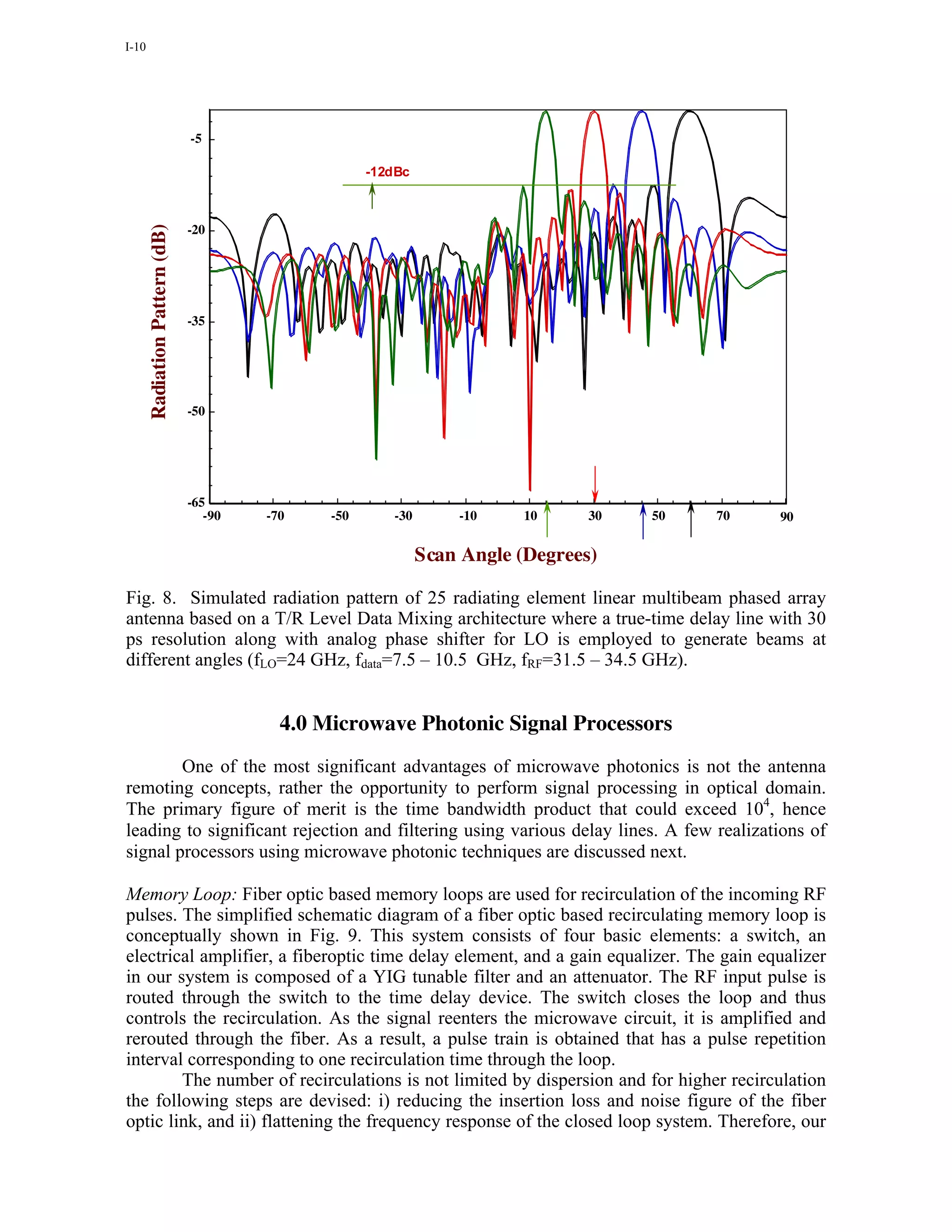
Fig. 7 depicts radiation pattern of a 25 element linear phased array (with λ/2
separation) designed for operation at center frequency of 33 GHz with bandwidth of 3 GHz
(i.e., each graph is composite of three simulated graphs at frequencies of 31.5, 33, and 34.5
GHz). The simulation results are for a CPU level data mixing. The required time delay is](https://image.slidesharecdn.com/en-028-all-120926115440-phpapp01/75/En-028-all-16-2048.jpg)
![I-9
achieved using a switched delay line TTD (true time delay device) with minimum time
resolution of 10 ps. As this simulation result indicates as the beam is pointed away from
broadside, sidelobe levels increase to only -6dBc and the main beam decreases by 2dB. On
the other hand, Fig. 8 depicts the simulated performance of the same phased array when it is
constructed based on T/R level data mixing. This structure employs a 2π analog phase shifter
based on the concept of cascaded oscillators [4] along with a TTD with a time resolution of
30 ps (i.e., decreasing the time delay number of bits by about factor of 4). As this figure
clearly represents no reduction in main beam peak level or the increase in side-lobe levels is
observed for any scan angles. In fact, the sidelobe levels are compatible with the expected
theoretical level of 13.6 dB for uniform array.
2dB
-5
-6dBc
-20
Radiation Pattern (dB)
-35
-50
-65
-90 -70 -50 -30 -10 10 30 50 70 90
Scan Angle (Degrees)
Fig.7. Simulated radiation pattern of 25 radiating element linear multibeam phased array
antenna based on a CPU Level Data Mixing architecture where a true-time delay line with10
ps resolution is employed to generate beams at different angles (fLO=24 GHz, fdata=7.5 – 10.5
GHz, fRF=31.5 – 34.5 GHz).](https://image.slidesharecdn.com/en-028-all-120926115440-phpapp01/75/En-028-all-17-2048.jpg)
![I-11
approach involves optimizing the performance of the fiberoptic delay element over the
bandwidth of 2-4 GHz. A fiberoptic link is established over 2-4 GHz with a measured
frequency response of the fiberoptic link has insertion loss of –11dB with flatness of 4dB
was. The fiberoptic link has a compression dynamic range of 134 dB.Hz and spurious free
dynamic range of 87 dB.Hz2/3. A low noise figure fiber optic delay element is capable of
recirculating a short electrical pulse as long as a millisecond, using 1 km optical delay line.
The spectral purity of the recirculated signal is evaluated using the phase coherency
measurement criteria. A plot of the phase noise degradation of the microwave carrier at three
different recirculation times and offset carrier is shown in Fig. 10, where the spectral purity
of the output pulses are shown after 10, 20, and 35 recirculations. The phase noise
degradation is measured for offset carrier frequencies of 10, 50 and 100 Hz.
SPDT Coupler
Amplifier
Switch
RF IN
RF OUT
Gain Equalizer
Delay Unit
Optical Optical
Receiver Transmitter
Fig. 9. Conceptual drawing of a fiberoptic based recirculating delay line. It is composed of a
SPDT switch, electronic amplifier, coupler, optical delay element, and gain equalizer.
Since the frequency response of the open loop is not, in practice, flat over the
bandwidth, for enhancing the performance of the memory loop, a gain equalizer is required.
The amplification of the recirculating signal can be realized in either the electrical [7] or the
optical domain. For broadband microwave signal processing, however, where the incoming
signals in the frequency range of 2-18 GHz are analyzed, pulse recirculation in the optical
domain is preferable to the electrical domain.](https://image.slidesharecdn.com/en-028-all-120926115440-phpapp01/75/En-028-all-19-2048.jpg)
![I-12
Fig. 10. Spectral purity and phase noise degradation compared to the input electrical pulse at
various offset carrier as a function of number of recirulations.
The most limiting factor that degrades the output signal of the optical delay element
is the noise build-up in the loop, whenever open loop gain is above unity. In particular,
flatness and the noise figure are the limiting factors of Fiber Optic Memory Loop (FOML).
The implication of non-flat frequency response of the delay unit is that the noise will
increase faster at frequencies where the loop gain is high. Therefore, the nonflat frequency
and high noise figure of the delay element will restrict the maximum number of recirculation
attainable by the memory loop. The maximum number of recirculations in the loop in terms
of the characteristics of the system components can then be numerically evaluated as a
function of gain flatness, C. Particularly, the maximum number of recirculations, nmax, is
limited to maximum number allowable by NFTmax, and the open loop noise figure NFB as
[7]:
n
NFTmax ≈ 1 (NFB-1) 1n 1-C +n
2 C 1-C
The implication of non-flat frequency response of the delay unit is that the noise will
increase at a faster rate at frequencies where open loop gain is greater than unity. Therefore,
the non-flat frequency response and high noise figure of the delay element will restrict the
maximum time delay attainable by the memory loop. Naturally, to overcome the nmax
limitation, while achieving long total time delays, nτ, one could increase the unit time delay,
τ, but the long unit delay will produce a void in the time domain for the short input pulses.
As an example, for the specified (S/N)out=10 dB in a fiberoptic based memory loop using a](https://image.slidesharecdn.com/en-028-all-120926115440-phpapp01/75/En-028-all-20-2048.jpg)
![I-13
commercial FO link (Ortel link depicted in Table II), the maximum number of recirculation
reduces from 954 for a flat frequency response to only 26 for a gain flatness of 1 dB.
Whereas in case of reactively matched optical transmitter, the maximum numbers are 3070
and 37, respectively, because of the lower loss and noise figure of the fiberoptic link. Using a
high gain reactively matched transmitter and an actively matched receiver leads to an
unprecedented number of recirculation. Once again as, the link flatness reduces to 1dB of
ripple, the maximum number of recirculation achieved would reduce to only 46 times. An
adaptive gain equalization technique can be used to suppress the effect of noise build up in
the system, which is enhanced by non flatness of the frequency response of the loop.
The maximum number of recirculation in the optical domain can be analyzed based
on the noise performance of the commercially available optical amplifiers. The noise build-
up in the optical system depends on many parameters such as optical power level, laser
modulation index, light coupling factors, and quantum efficiencies of electro-optic
transducers. Noise contribution of the spontaneous-spontaneous beat noise of the optical
amplifier to the overall noise can be minimized by a reduction of the enormous gain
bandwidth (>6000GHz) of the optical amplifier (to <100GHz).
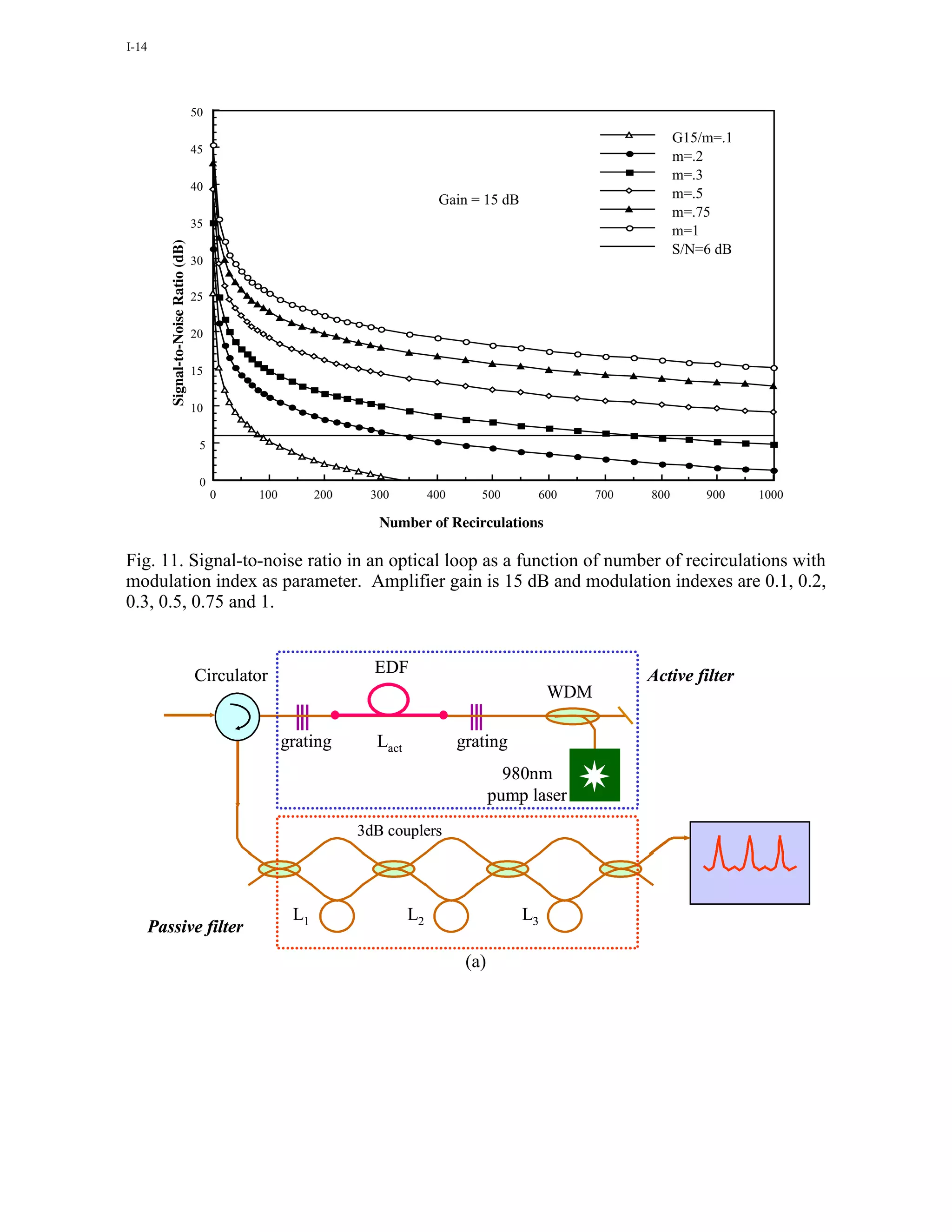
For the memory loop system with narrow optical bandwidth, the major noise source of the
system is signal-spontaneous beat noise. In this case, the maximum number of recirculations
in the optical memory loop is dependent on the signal level and modulation index of the
optical transmitter. As an example, a commercially available optical amplifier with the
following characteristics is considered. The optical amplifier has internal gain of 15dB,
saturation output power of 5 mW, noise enhancement factor of 2, and input and output
coupling efficiencies of 33%. The signal-to-noise ratio was calculated as a function of
number of recirculations with modulation index as a parameter. A plot showing the output
signal-to-noise ratio for the internal gain of 15 dB is depicted in Fig. 11. In this figure
modulation indexes of 0.1, 0.2, 0.3, 0.5, 0.75 and 1 are selected. Also shown here is the
output signal-to-noise ratio of 6 dB, which corresponds to the minimum signal-to-noise ratio
requirement for efficient detection. From this figure, based on a modulation index of 0.3,
and for signal-to-noise ratio to be degradated to 6 dB, the maximum number of
recirculations, as high as noptical= 750, is obtained. This number shows that when the
optical loop is operated at the proper bias and signal level for unit delay element of 1km,
time delay in the range of millisecond can easily be achieved. However, as the optical gain
increases, the number of optical recirculation diminishes precipitously.
Advanced Optical Signal Processing Techniques: The use of passive optical components
such as optical isolators, array wave guide grating, superposed array grating, and spatial light
modulators enable us now to perform a number of signal processing techniques to mitigate
interference [8- 10], and adaptive waveform generation [11]. The basic principle of these
techniques are based on translating spectrum to time using dispersive fibers or delay lines.
As the number of taps increases, increased resolution in frequency domain could be
observed. On the other hand, using mode-locke dpulses with short sampling period will
increase the time resolution. As the tap weights and unit time delay are adjusted, aribtary
waveform in time domain are generated that corresponds to the desired transfer function. Fig.
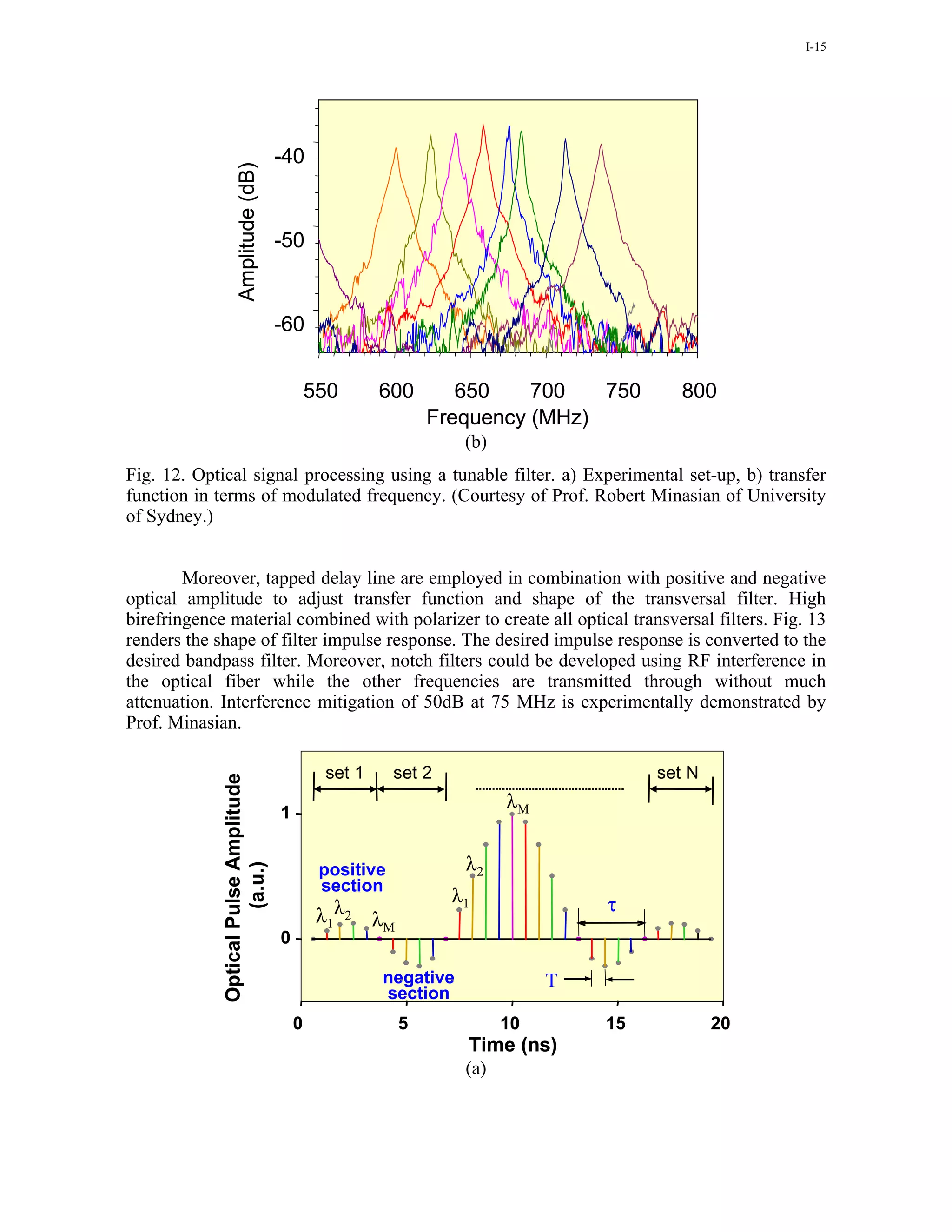
12 depicts structure of a tunable filter and a tunable filter Q as high as 800 has been
demonstrated by Prof. Minasian. Even though discrete grating arrays are simpler in design
and implementation, but for sampling bandwidth in the range of THz, superposed arrays are
quite practical [12].](https://image.slidesharecdn.com/en-028-all-120926115440-phpapp01/75/En-028-all-21-2048.jpg)
![I-16
Grating Positive Coefficient Section
Spectral Filters
Power τ Circulator λ1 λ2 λi λM
splitter
Photodetector
Time slot
Multiple Output
delay τ
Wavelength
Source
Photodetector
Negative Coefficient Section
Fig. Filter Impulse Response (FIR) using spectral time mapping. a) Desired signal in time
domain, and b) experimental set-up. (Courtesy of Prof. Robert Minasian of University of
Sydney.)
5.0. CONCLUSIONS
This paper provides a personal perspective of microwave photonics and its direction
of maturity. The direction of research is to develop novel devices that could meet high
performance and low cost expectation. The harsh military environment also impacts the
architecture of fiberoptic distribution networks. Among technologies that are unique to
microwave photonics is the issue of optical signal processing which could lead to very large
time-bandwidth products, hence resulting in high frequency selectivity. Memory loop
devices, transversal filters, tapped delay lines are attractive solution that commands nitch
market over the electrical signal processing techniques.
ACKNOWLEDGMENT
The author wishes to acknowledge the contribution of many of my students,
partciularly Dr. Reza Saedi, Dr. Xiangdong Zhang, Dr. Manocher Ghanevati. Author also
wishes to acknowledge contribution of Prof. Robert Minasian to the topics of transversal
filter and tapped delay line.
REFERENCES
[1] H.X. Shi, D.A. Cohen, J. Barton, M. Majewski, L.A. Coldren, M.C. Larson, G.A. Fish,
“Dynamics range of widely tunable sampled grating DBR lasers,” Electron Lett., Vol 38, pp.
180-181, Feb. 2002.
[2] A. S. Daryoush, K. Sato, K. Horikawa, and H. Ogawa, "Dynamic Response of Long
Optical Cavity Laser Diode for Ka-band Communication Satellites," IEEE Trans. Microwave
Theory and Techniques, Vol. 45, no. 8, pp. 1288-1295, August 1997.
[3] R. Saedi, W. Jen, N. Samant, A.S. Daryoush, D. Sturzebecher, P. Herczfeld, "Comparison
of CPU Level data Mixing to T/R Level Data Mixing Architectures in Optically Controlled
Phased Arrays," The 1993 International Microwave Symposium, Atlanta, GA, June 1993.
[4] X. Zhang and A.S. Daryoush, "Full 360o Phase Shifting of Injection Locked Oscillators,"
IEEE Microwave and Guided Wave Letters, vol. 3, no. 1, pp. 14-16, 1993.](https://image.slidesharecdn.com/en-028-all-120926115440-phpapp01/75/En-028-all-24-2048.jpg)
![I-17
[5] X. Zhou and A. S. Daryoush, "An Efficient Self-Oscillating Mixer for Communications"
IEEE Trans. Microwave Theory and Techniques, vol. 42, no.10, pp.1858-1862, Oct. 1994.
[6] A. S. Daryoush, K. Sato, K. Horikawa, and H. Ogawa, "Efficient Optoelectronic Mixing
at Ka-Band Using a Mode-Locked Laser," IEEE Microwave and Guided Wave Letters, Vol.
9, no. 8, pp. 317-319, August 1999.
[7] R. Saedi, A.S. Daryoush, and P. Herczfeld, "Fiberoptic Based Recirculating Memory
Loop" The 1992 IEEE International Microwave Symposium Digest, 1992 IEEE MTT-S
Microwave Symposium Digest, vol. II, pp. 677-680, Albuquerque, NM, June 1992.
[8] D.B. Hunter, R.A. Minasian, P.A. Krug, “Tunable Optical Transversal Filter Based on
Chirped Gratings,” Electron Lett., vol. 31, pp.2205-2207, 1995.
[9] J. Campany, D. Pastor, B. Ortega, “New and Flexible Fiberoptic Delay Line Filters using
Chirped Bragg Gratings and Laser Arrays,” IEEE Trans Microwave Theory Techn., Vol. 47,
pp. 1321-1326, 1999.
[10] X. Wang and K.T. Chan, “Tunable All-Optical Incoherent Bipolar delay-Line Filter
using Injection-locked FP laser and Fiber Bragg Gratings,” Electron Lett., vol. 36, no.24,
2000.
[11] A.M. Weiner et al, IEEE J. Quantum Electron, vol. 28, p. 908, 1992.
[12] R.A. Minasian, K.E. Alameh, and E.H.W. Cahan, “Photonics-based Interference
Mitigation Filters”, IEEE Trans on Microwave Theory & Techn., Special Issue on
Microwave and Millimeter-wave Photonics, Vol. 49, No. 10, pp. 1894-1899, 2001.](https://image.slidesharecdn.com/en-028-all-120926115440-phpapp01/75/En-028-all-25-2048.jpg)

![1-2
small part of the cavity, instead of modulation via the injected current, as usually made. To achieve such a
goal, the cavity of the semiconductor laser is separated into two parts: one is devoted to the laser gain, and
the second to the modulation (figure 1). It means that the p+ upper electrode of the laser is separated into
these two parts: a long one for gain purpose on which a current is injected, a short one for modulation on
which the microwave signal is applied. These two electrodes must be electrically isolated. Compared to
dynamic response of classical semiconductor laser, theoretical results [1] predicted a strong enhancement of
the resonance effects at the same frequency, with a lower decrease of the dynamic response at high
frequencies, 20 dB instead of 40 dB per decade (figure 2).
D. C. R. F.
InP P+
Grinsch MQW (1.55 µm)
InP N+
substrate (InP N+)
ground
Figure 1 : Two electrode laser diode for parametric modulation.
This device was fabricated at Thales TRT. It was an InP MQW DFB laser with two electrodes (same axis)
electrically isolated. Much attention was given to the isolation obtained by etching, and also to get low
parasitic contact resistance and capacitance of the short length modulation zone. Experimental results
confirmed theoretical predictions with the demonstration of a cut-off frequency over 30 GHz [2].
D. C. R.F.
REL. OUTPUT POWER (dB)
InP P+
Grinsch MQW (1.55 µm)
InP N+
substrate (InP N+)
ground
D. C. + R. F.
InP P+
Grinsch MQW (1.55 µm)
InP N+
substrate (InP N+)
ground
FREQUENCY (GHz)
Figure 2 : Direct modulation and parametric modulation characteristics of semiconductor laser diodes.
An alternative to this approach is the laterally coupled dual laser. This new solution is currently studied in
the frame of the FALCON TMR European project (coordination: prof. H. Lamela, university Carlos III –](https://image.slidesharecdn.com/en-028-all-120926115440-phpapp01/75/En-028-all-28-2048.jpg)
![1-3
Madrid). The principle is here to integrate inside the same laser cavity two parallel active zones. The first
fabricated prototype is a 1.3 µm MQW InP Fabry-Perot laser with two active regions defined by the two
parallel electrodes and by rib etching of the upper layer to get the optical confinement (figure 3). Depending
on the distance between the two ribs, the optical coupling between the two laser active zones can be adjusted.
GaInAs GaInAs
InP p +
Active layer (MQW)
InP n +
Substrate InP SI
Figure 3 : Schematic view of a laterally coupled semiconductor laser.
It was theoretically predicted that a strong enhancement of the bandwidth could be achieved by applying the
modulation current to one electrode and a DC current to the other one [3]. The bandwidth enhancement can
be explained by a phenomenon similar to the bandwidth increase of coupled oscillators. First experimental
results do not confirm theoretical bandwidth improvements. But a splitting of the optical modes into two
lines could be observed, the frequency separation depending on the electrodes biasing. This result can be
used to generate a microwave signal through the beating of the two optical modes into a high speed
photodetector. In this experiment, the frequency of the microwave signal could be tuned with the bias
currents injected into each active zone of the dual laser. The microwave signal frequency increased with the
difference between the two bias currents and was only limited by the cut-off frequency (18 GHz) of the high
speed photodetector. Nevertheless, due probably to the Fabry Perot multimode operation, the microwave
signal was not pure enough to be useful and DFB structures seem to be promising.
2.2 External modulation:
It is an interesting alternative to direct modulation. For this scheme a CW current is injected into the laser
diode and the modulation is applied to an external optical modulator. As a consequence the best (bias)
conditions can be used for each function (emission and modulation). To improve the noise, hence the
dynamic of the link, solid (YAG) lasers can advantageously replace the semiconductor (DFB) laser, if no
limitation in place is required. Among the effort to increase the performance of the optical modulators, the
bandwidth is an important feature. We can class modulators in two main types: electro-absorption and
electro-optic modulators. For the first type an electric field, modifies the transparency (or absorption) of a
III-V material for an optical signal wavelength close to its bandgap wavelength. Thanks to Franz Keldish
effect a change of bandgap energy occurs under applied voltage and for a good choice of signal wavelength,
the semiconductor material changes its transmission state from transparent to absorbing. Multiquantum well
PIN structures introduced into optical waveguides are used to increase this phenomenon (Quantum Confined
Stark Effect). With this kind of devices bandwidth above 40 GHz are obtained, combined to a modulation
voltage close to 1 V. The efficient modulation / voltage ratio is a consequence of a (resonant) exitonic effect
and thus the optical bandwidth of the modulator is limited to several 10 nm. In spite of a low modulation
voltage, which makes these devices attractive, they are in general strongly nonlinear and the quality of the
microwave optical link can be degraded.
It is the reason why electro-optic modulators, based on the modulation of the phase of the optical signal via
the electro-optic Pockels effect, is also under studies. To get an amplitude modulation, the electro-optic
device is based on the principle of the Mach-Zehnder interferometer: the optical signal is divided into two
arms (equal length) and recombined at the output. The device is fabricated in integrated optics, with an
electrooptic material. Electrodes are placed along one (or both) arms. When a voltage is applied to one arm, a
corresponding optical phase change is obtained; if the difference of phase at the output of the two arms is π,
a null occurs (which defines Vπ voltage). Different materials are used: LiNbO3, III-V, polymers... LiNbO3](https://image.slidesharecdn.com/en-028-all-120926115440-phpapp01/75/En-028-all-29-2048.jpg)
![1-4
exhibits the highest optical index variation with electric field. Even in this case, the electrode must be long
(over 1 cm) to get a Vπ voltage still rather high (~10V). The consequence is a high capacitance, and the only
solution to overcome this fundamental limitation is the travelling wave electrode. The basic idea is here to
transform the long electrode into a 50 Ω transmission line loaded on a 50 Ω impedance. In principle, if the
optical and microwave indices are equal, the bandwidth is unlimited. This is difficult to achieve with LiNbO3
because the microwave permittivity is far from the square of the optical index; for III-V materials the
condition optical index # microwave index is verified but these materials suffer from a lower electro-optic
effect. Polymer based modulators are under intense research because optical and microwave indexes are
equal and polymer can be deposed on metal leading to, in principle, ideal microwave microstrip lines.
Electro-optic effect is induced by chromophores introduced in the polymer. To get an electro-optic activity, a
poling procedure is carried out. Bandwidth over 40 GHz are obtained with the three types of materials. Due
to a special electrode design (LiNbO3 modulators) or advanced materials (polymer modulators), low Vπ (< 1
V) and high bandwidth electro-optic modulators are demonstrated [4, 5].
2.3 Optical control of microwave oscillators :
It consists of modifying the characteristics (amplitude, phase or frequency) of a millimetre wave signal
generated by the oscillator, thanks to the optical signal impinging on the oscillator. It is also possible, to
optically lock the frequency of the microwave oscillator. In optical injection locking, the optical control
signal is intensity modulated at a frequency close to the free running frequency of the oscillator (fundamental
locking), one of its harmonics (harmonic locking), or one of its subharmonic (subharmonic locking) [6]. The
modulated optical signal absorbed in the device active region gives rise to a current flow at the modulating
frequency, and this acts in a very similar way to direct microwave signal injection. The use of subharmonic
locking is suggested by the inherent nonlinearity of the active devices composing the oscillator, and it allows
to use a diode laser which cut-off frequency is far below the frequency of the microwave oscillator (also with
the possibility to neglect fibre dispersion effects). A fibre radio link was recently demonstrated based on this
principle, with 7.6 dBm microwave output power, the oscillator being locked using up to the 32th
subhamonic. The frequency was 10.6 GHz and the wavelength was 0.8 µm, the link being composed of a
GaAs VCSEL and a GaAs MMIC [7]. Because this technique is promising for simplicity, power, conversion
efficiency, intensive research are devoted to this topic for 1300 and 1550 nm operation, or for example at
University of Kent at Canterbury.
2.4 Generation of harmonics with laser non-linearities:
When biased under high current or modulated at a frequency close to the resonance frequency, a laser diode
is generally highly non-linear. This effect can be advantageously used to get harmonics of the modulating
microwave signal at the output of the link, if the speed of the photodetector is high enough and the length of
fibre low enough to overcome bandwidth limitations due to fibre dispersion effects. In practice, the laser bias
current is adjusted to match the resonance frequency of the laser to the microwave modulating frequency to
improve harmonics generation ; an electrical filtering at the output of the photodetector allows to select the
good harmonic. In terms of phase noise, the degradation (20.Logn, where n is the rank of the harmonic) is
similar to a system based on the transmission of the fundamental through the link and electrically multiplied
at the output, (or other systems based on a reference multiplication). For both cases, fibre-radio systems were
demonstrated [8, 9], the second solution being more tolerant to the fibre dispersion, but a more complex
microwave circuit (MMIC) is required. In principle this method could be extended to non-linear
photodetectors. But a photodetector (except for very small ones) is a very linear component compared to a
laser diode. Non-linear photodetector behaviour needs high optical power and low bias voltage and in
practice in a link, laser diodes non-linearities appear before photodetector ones.
2.5 Dual mode emitters:
Another class of the optical microwave or mm-wave generation techniques is based on the emission of an
optical spectrum consisting of only two discrete tones, separated by the mm-wave frequency. Mixing the two
phase-correlated tones at a square low photodetector provides a spectrally pure mm-wave carrier signal at
frequency fmm. Fiber dispersion only affects the phase of the detected mm-wave signal, and this approach can
operate over arbitrary lengths of standard fibre at 1550 nm.](https://image.slidesharecdn.com/en-028-all-120926115440-phpapp01/75/En-028-all-30-2048.jpg)
![1-5
A well-known system is the one adopted within the FRANS project, supported by the European Commission
ACTS programme, and developed within the RACE project MODAL [10]. This technique generates a two-
tone optical signal using a Mach-Zehnder modulator as an electro-optic mixer. Knowing that the Mach-
Zehnder Modulator has a raised cosine intensity response, when biased at the point of minimum optical
transmission, the response of the device on the optical field can be written as : Eout = Ein sin (π V/2Vπ ) [11],
leading to two optical modes.
Among the number of approaches which have been proposed and demonstrated to optically generate mm-
wave signals [see for example 12 – 32], a very promising solution based on optical heterodyning, was
developed at BT Laboratories. It consists of a master-slave Distributed Feedback (DFB) laser arrangement,
where the lasers are in a series configuration and each laser contributes a single mode for optical mixing in a
high speed photodiode [25, 32]. The electrical drive to the slave laser is at a subharmonic of the beat
frequency and generates a series of sidebands. The master laser mode injection locks one of these slave
sidebands which results in phase noise cancellation in the output signal.
It is also interesting to mention the works on optical Single Side Band generation to overcome penalties in
fibre radio system with data signal. It has been demonstrated that, by using an optical filter to suppress one of
the sidebands [33], in intensity modulation schemes, dispersion effects can be reduced by the elimination of
one sideband to produce an optical single-sideband. This method is limited by the filter characteristics and
can be quite complex to implement. To eliminate the need of optical filtering, a novel technique recently
proposed [29] uses only one dual-electrode Mach-Zehnder Modulator. The RF signal is applied to both
electronics with π /2 phase shift applied to one electrode. A DC bias voltage is also applied to one electrode
while the other DC terminal is grounded. The Mach-Zehnder modulator can be considered as two optical
phase modulators in parallel with drive signal π /2 out of phase and with DC voltage applied to one arm. By
tuning the DC voltage, modulator is biased at quadrature. The RF power degradation due to fibre dispersion
was observed to be only 1.5 dB when using the technique to send 2 – 20 GHz signals over 79,6 km of fibre.
Approximately at the same time, fully integrated millimetric single sideband lightwave source were
demonstrated [30] increasing the attractiveness of this technique.
Obviously the disposal of monolithic integrated dual mode sources is interesting for compactness, reduction
of parasitics, efficiency... One way, as said just before [30], is the monolithic association of a DFB laser and
a specially designed external optical modulator. One other way is the dual mode laser. DFB laser structures
for which the usual effort to lift the mode degeneracy was not taken into consideration are dual mode laser.
The coupling coefficient and the total laser length are the two main parameters governing the frequency
separation between the two modes. The mode separation is approximately given by the following
expression: ∆f ~ 1.5 c κ 2 / (π ne tanh(κL))
Where ∆f is the mode frequency separation of the DFB ; κ the coupling coefficient of the DFB structure and
L the total laser length. For a 60 GHz mode separation for example, we need a 2 mm long laser with a 9 cm-1
coupling coefficient. To reduce the laser length we need to reduce the coupling coefficient as well (below 3
cm-1 for a 1 mm long laser). But it seems difficult to control such reduced coupling coefficients from a
technological point of view and the laser could possibly turn into a multimode emission. A possible structure
designed with the aim of reducing the “effective” coupling coefficient using usual technologies compatible
with conventional coupling coefficients, consists of alterning DFB and FP sections pumped by a single
section source (figure 4). Using such a structure we can expect to get a reduced effective coupling coefficient
by increasing the FP section length. A square wave function will sample the DFB structure according to its
duty cycle. So, the refractive index of this structure will be equal to the refractive index of the conventional
DFB multiplied by the Fourier series expansion of the spatial square wave function. It turns out that instead
of having a single reflection coefficient centred around the Bragg frequency, this structure will generate a
periodic filter with a periodicity in terms of optical frequency.](https://image.slidesharecdn.com/en-028-all-120926115440-phpapp01/75/En-028-all-31-2048.jpg)
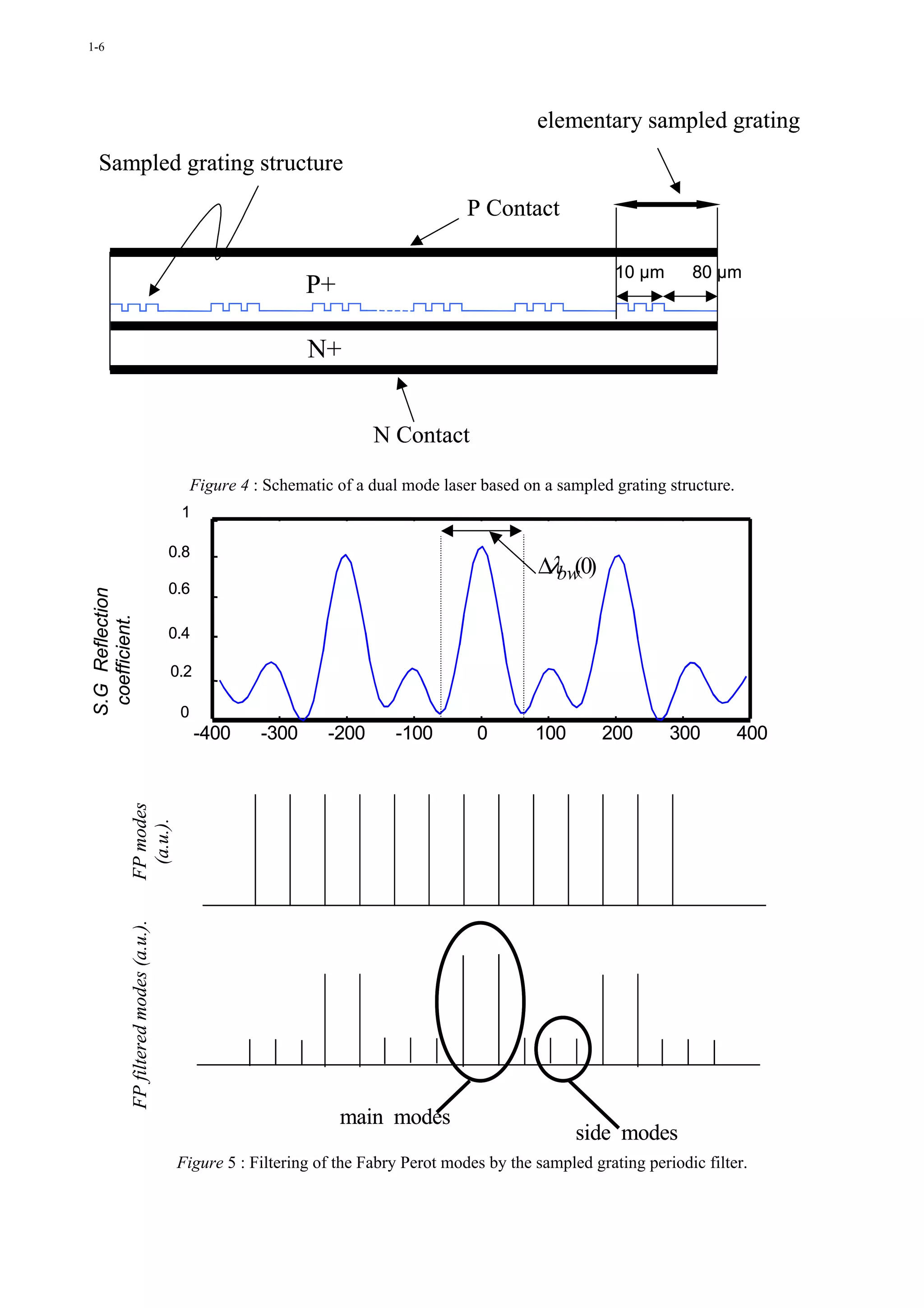
![1-7
This can be illustrated by the schematic given in figure 5 where we show the modes of a Perot Fabry cavity
and we superimpose the filter due to the periodic DFB section. Such a structure was modelled using the time
domain model. It was shown that a good design of this structure predicts theoretically a dual mode emission
with 60 GHz optical frequency separation and a dual-side mode suppression ratio of more than 35 dB [34].
3. Optical switching matrixes
An interesting example of microwave applications using optics is optical phased array antenna control. The
emerging direction of array antenna beam depends on delays or phases laws. It is defined by the path
differences between the physical plane of the radiating components and the virtual plane perpendicular to the
beam direction.
Delays, instead of phase shifts, are needed to insure frequency independent beam steering. Usually, true time
delays are obtained by the use of coaxial links or microstrip lines. In this case, the limitations are antenna
dimensions and instantaneous bandwidth. Optoelectronics is one of the most promising techniques that
allows antenna to fit both aerodynamic requirements and whole space survey. Different methods were
proposed : for example the use of high dispersion fibre in conjunction with a widely tunable optical source to
obtain the required delay variation [35], or systems where polarisation switching spatial light modulators
route the optical path directly or via a corner reflector to select the delay [36]. In one system studied by
Thales TRT, signal delay is optically obtained by associating switching matrixes with fibres of different
lengths. Architecture properties are characterized by both temporal dynamic and resolution. Due to losses,
the critical point in such systems is the number of fibre to waveguide interfaces. Thus, in order to reduce
losses one possible solution is to use architecture based on high order matrixes.
Numerous optoelectronic laboratories are currently enhancing technology and properties of such devices. In
particular, Westinghouse has developed a true time delay system using microwave and optical technology
[37]. Thales TRT proposes a system based on integrated switching matrixes. The use of guided optics allows
high order matrix implementation. Moreover, light offers an additional dimension which is wavelength. If
matrixes are strictly non-blocking, which means that each input can be connected to each output
independently, this dimension allows a reduction in the number of switching components proportional to the
number of optical wavelengths. With this architecture, it is possible to achieve more than 4000 different
paths with four 8*8 matrixes. It is characterized by a temporal dynamic of 4 ns for a resolution of 1ps.
Key components of this system are switching matrixes that fit the following specific conditions:
light polarization insensitivity
strictly non blocking matrix
equivalent intra-matrix path lengths
low power consumption.
low insertion loss
low excess noise (phase noise)
low cross-talk
short switching time
Due to high speed switching requirements, electro-mechanical (MOEMS) or thermo-optic effects (polymers)
cannot be used to fabricate the switching active elements. Semiconductor optical amplifiers (SOA) is an
attractive way because of its capability to high cross-talk, compensation of insertion losses and high speed.
But recent experiments performed at Thales TRT shown that this component increases strongly the phase
noise of microwave signals [38]. Consequently solutions using electro-optic switches driven by electrostatic
modulation, carriers depletion or injection must be explored.
Among possible materials, InP based are well established for 1.3 or 1.55µm wavelength applications. An
optical switching matrix is a photonic integrated circuit associating monolithically passive elements (optical
waveguide with bendings,…) and switching active elements. As an example, an InP optical waveguide,
grown by MBE or MOCVD on n type InP substrate, is constituted of a GaInAsP quaternary core layer
inserted between InP confinement layers with a lateral confinement obtained via a rib etching (figure 7).](https://image.slidesharecdn.com/en-028-all-120926115440-phpapp01/75/En-028-all-33-2048.jpg)
![1-8
4 µm
0.7 µm InP
0.5 µm
0.2 µm 1.15 µm InGaAsP
InP
Figure 7 : Example of optical InP passive waveguide for switching matrixes.
About active elements, we used in devices fabricated at IEMN the plasma effect, obtained by injection of
carriers in the optical waveguide, thanks to a PIN structure located by etching in the active zone. This effect
decreases the optical index almost linearly with the density of carriers (≅10-3 for 1017 cm-3). We studied
different structures : a kind of Electro-Optical Directional Coupler (EODC) that we called "cascade switch"
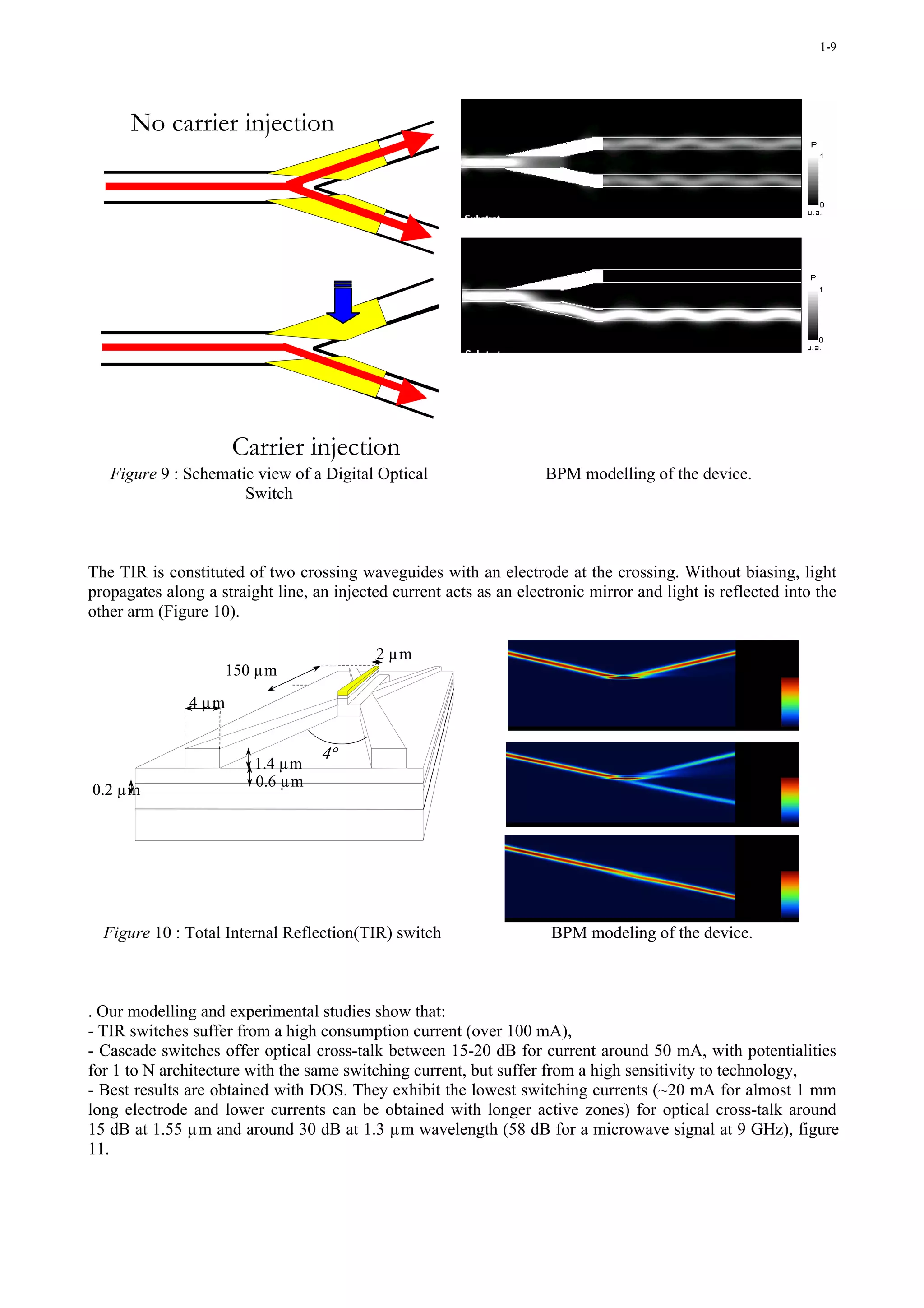
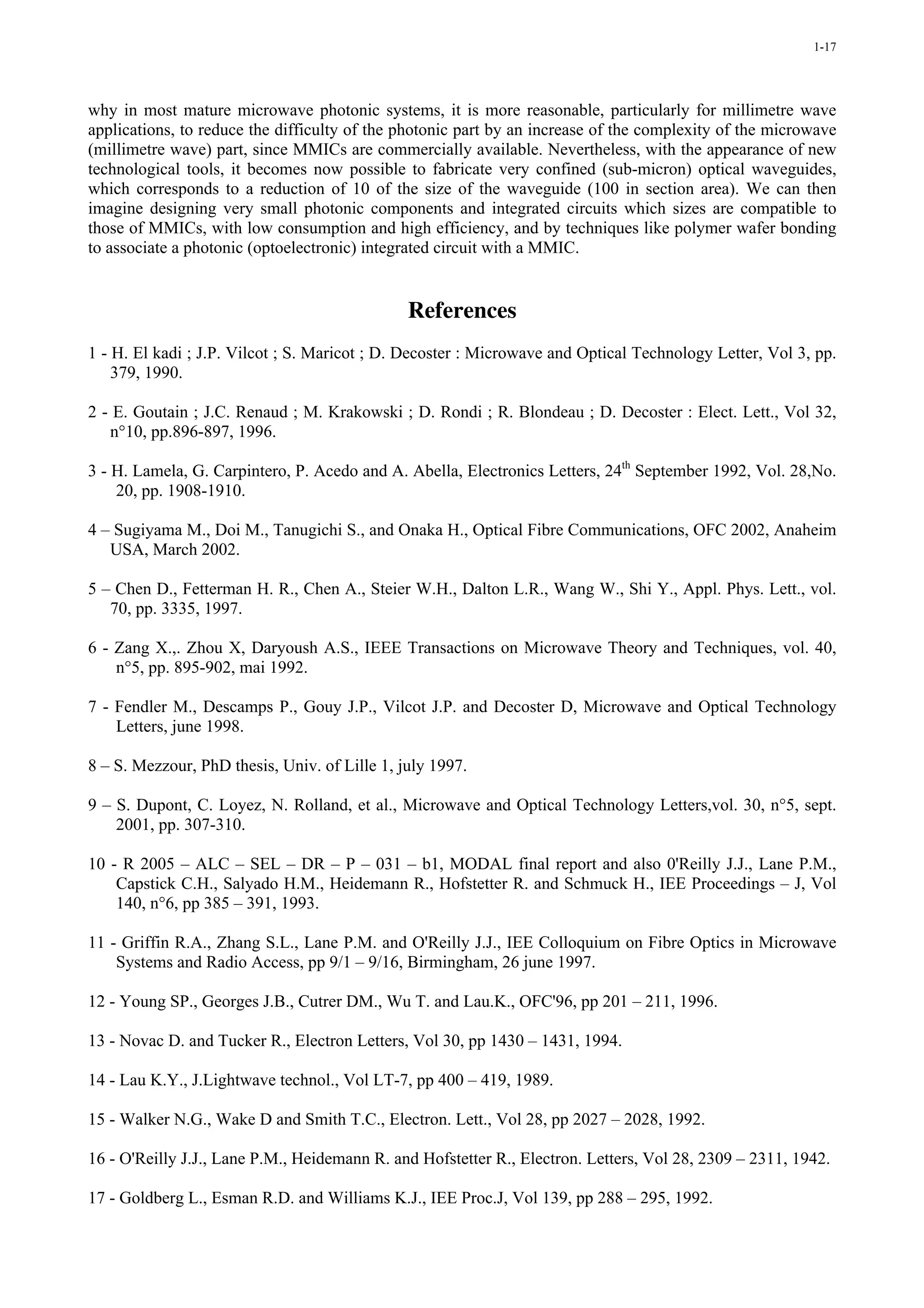
[39-40] based on mode coupling, Digital Optical Switches (DOS) based on adiabatic mode changes [41] and
a Total Internal Reflection (TIR) switch based on high reflection [42]. A 1 to 2 cascade switch (1 input, 2
outputs) is constituted of one active PIN waveguide placed closely between two passive waveguides playing
the role of 1 input and 2 outputs. When no current is injected, the optical input beam is coupled to the
extreme output waveguide. If current is injected into the current injection zone, the coupling is cancelled and
light goes on the waveguide located just before the injection zone, here the input waveguide. This scheme
can be extended to 1 to N optical switch: only one current injection will be required to obtain the light switch
to any of the N outputs (figure 8).
Figure 8 : Schematic view of a cascade switch Modelling of light propagation (2D Beam
Propagation Method) inside a cascade switch.
The technological fabrication [40] allows the monolithic integration of active and passive zones and is
composed of three main steps: p ohmic contact realisation of the current injection zone, etching of the
different guides, first level metallization and thinning and back N-metallization. The DOS is a Y junction
with an electrode on each output arms. Without bias current the light is divided equally between the two
arms. When a bias current is injected into one arm, optical index is reduced in this region, and light is pushed
toward the other arm (figure 9).](https://image.slidesharecdn.com/en-028-all-120926115440-phpapp01/75/En-028-all-34-2048.jpg)
![1-10
Electrical detected output power
Electrical detected output power
-40 -40
-50 -45
-60 -50
(dBm)
(dBm)
-70 -55
-80 -60
-90 -65
-100 -70
-110 -75
0 5 10 15 20 0 5 10 15 20 25
Injected current (mA) Injected current (mA)
Figure 11a: Electrical output power of a 9 GHz signal Figure 11b: Electrical output power of a 9 GHz signal
issued from the switched on DOS branch (solid line) issued from the switched on DOS branch (solid line)
and the switched off one (dashed line) @ 1.3µm. and the switched off one (dashed line) @ 1.55µm.
The difference between 1.55 µm and 1.3 µm wavelength cross-talk can be explained by band filling effects
occurring for an operation wavelength close to the quaternary core layer bandgap wavelength [41] At last it
was experimentally checked that the phase noise is not degraded by using DOS as shown on figure 12.
-60
-70
Noise power (dBc/Hz)
-80
-90
-100
-110
1 10 100 1000
Frequency from the carrier (kHz)
Figure 12 : Noise power level for at 9 GHz carrier@ 1.3 µm :
- gray line: switched signal (DC bias = 20 mA)
- black line: direct signal (DC bias = 0 mA)
4. High speed photodetectors
It is well known that high speed PIN photodiodes require short transit time in the active layer and small
capacitance. As a consequence, for very high speed (millimetre wave) applications, the absorbing GaInAs
region of InP photodiodes must be thin, typically 0.4 µm and less for cut off frequency higher than 60 GHz.
With vertical illumination so thin absorbing layer leads to small quantum efficiency (figure 13a). The well
known solution to overcome this trade off is the lateral illumination [43]. The photodetector is similar to an
optical waveguide with an absorbing core, and is called PIN waveguide photodetector (figure 13b).](https://image.slidesharecdn.com/en-028-all-120926115440-phpapp01/75/En-028-all-36-2048.jpg)
![1-11
hν p type ohmic contact
n type ohmic contact
p type ohmic contact
n type ohmic contact
E p+
E p+ nid
nid dabs n+
Edge illumination hν S.I.
hν
n+
S.I.
Figure 13a : Schematic view of a top illuminated Figure 13b : Schematic view of a PIN waveguide
PIN photodiode photodiode
4.1 First problem: the optical coupling.
To get a good coupling to the optical fibre, a multimode structure is more suitable (figure 14). A typical
epitaxy on InP semi-insulating substrate is then: a nid GaInAs absorbing layer between two (n and p types)
GaInAsP and InP confinement layers, with a GaInAs p-type contact top layer. As an example, devices
fabricated at IEMN exhibit a 4 µm etched rib waveguide, an input facet obtained by cleaving, with a total
device length ranging around 10 to 20µm. With a lens-ended fibre, quantum efficiency higher than 60%
without anti-reflection coating can be achieved with cut-off frequency over 60GHz [44].
Rib : 3.5 µm×20 µm
InP P (>1018 At/cm3) 0.5 µm
GaInAsP (1.3 µm) P (5.1017 At/cm3)
1.5 µm
GaInAs N (5.10 15 At/cm3) 0.3 µm
GaInAsP (1.3 µm) N (>1018 At/cm3) 1.5 µm
InP N (>1018 At/cm3) 0.2 µm
Figure 14 : multimode waveguide PIN photodiode
4.2 Second problem: the microwave or millimetre-wave access.
A semi-insulating substrate and a coplanar line improve the microwave access, by reduction of parasitics
(capacitance …) (figure 15). The semi-insulating substrate allows the monolithic integration of a passive
reactive network with the PIN waveguide photodiode to reduce the large impedance mismatch between the
PIN photodetector and the 50Ω of the microwave world in a small bandwidth, as experimentally
demonstrated for 30 GHz operating frequency by Thales TRT, in collaboration with IEMN [45].](https://image.slidesharecdn.com/en-028-all-120926115440-phpapp01/75/En-028-all-37-2048.jpg)
![1-12
Coplanar access photodiode surface area: 3 µm x 15 µm
ht
Lig
40 fF photodiode
300 pH serial inductor
capacitance
Figure 15 : coplanar microwave access. Monolithic integration of
PIN waveguide photodiode and inductor
4.3 Third problem: the power.
Power limitation (≅ 0dBm at 60GHz) [46] occur in so small devices, due to high density of photocarriers
killing the electric field in the intrinsic region and high photocurrent reducing the bias voltage in the external
circuit. These effects reduce the dynamic of the link. To solve this problem, two ways are possible : the
travelling wave photodetector with a long length (and hence volume) with electrodes designed to get a 50Ω
microwave line, and the uni-travelling carrier photodetector (figure 16) for which photodetection takes place
in a thin p-type highly doped GaInAs absorbing layer. Up to date results are very encouraging [47, 48] and
works are in progress at IEMN in collaboration with Thales TRT and Alcatel to get high speed, high power
and high quantum efficiency devices.
Barrière Absorption Collecteu r Su b-collecteu r
Energie
- - Dérive
hν
+
+
Compen sation diélectriqu e
X
Figure 16 : band structure of an UTC photodiode.
Only electrons pass through the collector.
4.4 Fourth problem: the reliability.
The direct illumination scheme used in these devices has some known impairements: input facet fabrication
with junction passivation is difficult to achieve with high reliability [49]. To overcome these impairments,
high speed edge illuminated, evanescently coupled PIN photodiode was demonstrated [50]. For this last
device, a taper was included in the input waveguide, leading to better alignment tolerance to the fibre. But
the tapered waveguide exhibits excess loss which reduces the sensitivity. It is the reason why an attractive
way is the use of a diluted multimode input waveguide, followed by the evanescently coupled PIN
photodiode. The diluted waveguide is made of very thin GaInAsP quaternary epilayers introduced in InP.](https://image.slidesharecdn.com/en-028-all-120926115440-phpapp01/75/En-028-all-38-2048.jpg)
![1-13
The distance between the quaternary epilayers decreases from the substrate to the top of the waveguide to get
a specific waveguide which can be compared to a half lens whose centre is on the top of the waveguide
(figure 17). Due to numerous technological parameters and targeted performances, the device was optimised
at IEMN using genetic algorithm coupled to a 2D – BPM [51]. It was fabricated at Opto+ and experimental
results shown that high responsivities (≅ 1 A/W), low polarisation dependence (<0,5 dB) and high alignment
tolerance (≅ ± 2µm) can be achieved at 1,3 and 1,55µm wavelength [52]. The cut-off frequency is in excess
of 3GHz and works are in progress to extend the bandwidth up to the millimetre wave frequency range.
P+ InP
nid GaInAs
N+ GaInAsP
N+ GaInAsP
N+ InP
1.3 µm N+ InP
N+ GaInAsP
N+ GaInAsP
or N+ InP
1.55 µm N+ GaInAsP
N+ InP
N+ GaInAsP
N+ InP
Figure 17 : multimode evanescent coupled PIN waveguide.
5. Specific microwave photonic functions: up and down conversion
5.1 Principle:
Up or down conversion is based on the existence of a non-linear element in a circuit. This element can be
purely electrical and associated to the optical (or optoelectronic) component or circuit, or inside the
optoelectronic component itself. We will examine various examples of non-linear functions at the emitter
stage or receiver stage, demonstrating their ability for up or down conversion. The characteristic parameter is
the gain conversion, which represents the comparison between the intensity of the converted line to the
signal line. The goal is here to get a gain conversion (and hence a non-linearity) as high as possible.
5.2 Emitter stage:
Semiconductors lasers can be non-linear (under particular conditions such as high bias current or signal
frequency close to the resonance frequency) but their characteristics are also degraded (noise...). To enhance
non-linear effects and keep a good quality of emitted signals, other solutions are possible such as the
association of a laser diode with an external modulator. The microwave signal is applied onto the laser and
the second one onto the optical modulator. By doing this, the amplitude of the optical signal is modulated
two times and contains the product of the two microwave signals amplitude. As a consequence, we find at
the output of a high speed photodetector the two lines of the applied microwave signals, but also the sum and
the difference of these two frequencies. Derived solutions are for example based on the use of one CW laser
diode associated with two external modulators in series to apply the microwave signals. Monolithic solutions
are also possible with (commercially available) DFB laser integrated with an electroabsorption modulator.](https://image.slidesharecdn.com/en-028-all-120926115440-phpapp01/75/En-028-all-39-2048.jpg)
![1-14
Another monolithic possible solution is the use of two-electrode lasers presented in section 2 for their
enhanced dynamic response. The basic principle is to apply a microwave signal on each electrode with
frequency respectively f1 and f2. Since the power-current characteristic depends strongly on the voltage
applied onto the short electrode, the output signal will be strongly non-linear and at the output of the
photodetector we measure the beat between the two frequencies. Our experiments have shown that the
conversion gain ranges from -3 dB to –17 dB [53].
5.3 Receiver stage:
Photodetectors are in general linear devices (except under high power and low bias voltage, see before). It
means that it seems difficult to use them directly as up or down converters. It is the reason why most of the
solutions at the receiver stage are based on the association of a specific electrical (microwave) circuit to the
photodetector. The optoelectronic component is then considered as a microwave signal source and the up or
down conversion is made electrically with classical microwave techniques. Since many optoelectronic
components are now based on InP materials (1.55 µm and 1.3 µm wavelength), their monolithic integration
with microwave circuits (MMIC) is impossible, except if devices suitable for 0.8 µm wavelength are
accepted. As an example, a possible solution is a specific integrated circuit associating Metal-
Semiconductor-Metal GaAs photodetector with a dual gate MESFET. In spite of a rather low quantum
efficiency due to shadow effects of electrodes, GaAs MSM photodetectors are known as high speed devices
for 0.8 µm wavelength applications, with easy monolithic integration with field effect transistors. The use of
dual gate MESFET allows to enhance the non-linear effect of the transistor and to separate the two input
ports corresponding to the two microwave signals to be mixed. In this MOMIC (Microwave Optical
Monolithic Integrated Circuit) fabricated at IEMN, one gate is electrically connected to one electrode of the
MSM exactly as a PIN-FET and the other gate is used for the second microwave signal. The ability of this
integrated circuit to up or down convert the frequency of microwave signal modulating the optical signal
detected by the MSM photodetector was experimentally demonstrated [54] with conversion gain around –3
dB at 10 GHz.
The objective to monolithically integrate the non-linear microelectronics with the photodetector whatever the
optical wavelength (0.8 µm, 1.3 µm or 1.55 µm) is, led to use an heterojunction phototransistor (HPT) as
optoelectronic mixer. This device can be considered as a high speed photodetector with internal gain due to
transistor effect. It is also an heterojunction bipolar transistor (HBT) with a base-collector junction used as a
photodiode and combines monolithically the properties of an HBT and a photodiode. High speed transistor
and photodetector are obtained with short transit time in GaInAs p+ base and n- collector layers. Although
high speed demonstrations were made with top illuminated devices, edge illumination is suitable for high
quantum efficiency and millimetre wave operation. Following previous works [55], this scheme was adopted
at IEMN, since epilayers structures are compatible with an optical waveguide. For the devices fabricated at
IEMN, a GaInAsP quaternary layer was introduced between GaInAs collector and InP sub-collector to get a
multimode waveguide, figure 18. No quaternary layer was introduced in the emitter-base junction to keep its
electrical properties. As expected, this device is a millimetre wave photodetector with internal gain (≅5dB at
40GHz) and high quantum efficiency (60% without AR coating) [56, 57]. But it is also an efficient
optoelectronic mixer thanks to the non-linear behaviour of the transistor under suitable bias voltage [56, 57,
58]. More precisely, experiments carried out with a 1 GHz modulated optical signal, different optical powers
(from 0 to 1 mW at the output of the fibre) and electrical DC base bias currents, shown an improvement of
more than 30 dB for very small optical powers which can be explained by the gain non-linearities of the
device.](https://image.slidesharecdn.com/en-028-all-120926115440-phpapp01/75/En-028-all-40-2048.jpg)
![1-15
InP
Emitter
1.5 µm
InGaAs Base
Polyimide Emitter Base
InGaAs Collector InP InGaAs
Collector
InGaAs
InP Substrate
Figure 18 : Schematic view of a heterojunction Band structure of a heterojunction phototransistor.
phototransistor with base contact (3T-HPT).
These non-linearities can be used to mix an amplitude modulated optical signal with an electrical one applied
on the base terminal. Figure 17 shows the result of such an experiment. The intermediate frequency (IF) of
the modulated optical signal is 1 GHz (with a 10 dBm power on the laser) and the local oscillator frequency
(LO) is 18 GHz (with a power level of -20 dBm applied on the base). The electrical spectrum exhibits the
central band at 18 GHz and the two first sidebands at 17 GHz (LO-IF) and 19 GHz (RF=LO+IF).
Another experiment was carried out with IF=8 GHz (0 dBm on the laser) and 500 MHz < LO < 10 GHz
(with a power level of -10 dBm). The up-conversion gain (compared to the base-collector junction) versus
LO and LO+IF is presented on figure 19. The HPT optoelectronic mixer exhibits a 6 dB up-conversion gain
around LO=500 MHz and gain can be observed up to LO=7 GHz.
Figure 19 : Conversion gain (compared to the base-collector junction) of the mixing between an optical
signal modulated at IF=8 GHz and an electrical signal applied on the base modulated at 500 MHz<LO<10
GHz (power level of -10 dBm).
For comparison, Lui, Seeds and Wake [58] reported down-conversion using a two-terminals edge-coupled
InP/InGaAs HPT, with a maximum 7 dB down-conversion gain when IF=500 MHz, RF=2.5 GHz and LO=3
GHz. Suematsu et al. [59] reported a top-illuminated three-terminals HBT up-converting mixer with a
conversion loss of 4 dB when IF=3.2 GHz, RF=30 GHz and LO=26.8 GHz. These experiments show that
InGaAs / InP HPTs are promising devices to transmit a data signal up-converted to a millimetre-wave signal
thanks to a mixing with a signal delivered by a local oscillator. More recently, C. Gonzales [60] and G.
Eisenstein [61] demonstrated also very efficient mixing experiments using HPTs.](https://image.slidesharecdn.com/en-028-all-120926115440-phpapp01/75/En-028-all-41-2048.jpg)
![1-16
6. Hybrid versus monolithic integration
Microwave Monolithic Integrated Circuits are now fabricated in GaAs foundries and allow to associate, on
the same substrate, a lot of different passive or active components, to get a given or several microwave
functions on the same chip. Monolithic integration leads to a lot of advantages : compactness, reduction of
parasitics, increasing functionality... and we could hope to get the same advantages from the monolithic
integration of optoelectronic or photonic components, with microwave components to get Microwave
Optoelectronic Monolithic Integrated Circuits (MOMICs). This is possible in pure microwave circuits
because there is a technological compatibility (epitaxy, process...) between the various components of a
MMIC. Unfortunately, this technological compatibility does not exist between the various optoelectronic
(and microwave) components. For example, the structure of a high speed laser is completely different to the
one of a PIN photodetector or field effect transistor. It is the reason why, in spite of a lot of technological
works and researches in this field, it exists only a few examples of mature (industrial) photonic or
optoelectronic integrated circuits. A well known (and may be to date the only), commercially available
photonic integrated circuit, is a DFB laser integrated to an electroabsorption modulator. Even in this modest
circuit (two components) complex technological steps are required. Optoelectronic circuits, associating
optoelectronic components and microelectronics are not commercially available. This situation is due to
completely different epitaxial structure for the optoelectronic components (2-3 µm thick) and
microelectronic components (0.1 µm thick for a field effect transistor). The most advanced optoelectronic
integrated circuits are probably those based on the integration of an Heterojunction Phototransistor and
Heterojunction Bipolar Transistor, because these devices have the same structure, except some geometrical
aspects. Here the epitaxy and the process are almost the same. The difference between microelectronic and
optoelectronic devices is controlled by the design of the mask. Several high speed photoreceivers and non
linear photo-mixers or photo-oscillators were experimentally demonstrated, but up to now, to our knowledge,
no optoelectronic integrated circuit is commercially available.
The consequence is that optoelectronic industry has chosen the way of self-aligned flip-chip mounting
technique on silicon mother-board. The basic idea is here to fabricate each component (optoelectronic,
photonic...) needed for a circuit, using mature single component technology and to assemble them on a
specific silicon substrate. The main problems are then: how to align the optical (optolectronic) components
along the same optical axis and how to make the electrical (microwave) connections.
The first difficulty was solved using preferential silicon etching. The silicon substrate carries preferentially
etched V-grooves with the angle α =54.74° between the (100) and (111) crystal planes. Passive alignment of
single mode fibre and waveguide devices can then be achieved. Photolithography of Si mother board allows
the precise etching of V-grooves for the fibre alignment and other V-grooves for the positioning of the
waveguide device. To get the alignment compatibility of the photonic device with the silicon mother board,
special alignment indentation, self aligned with the waveguide stripes are achieved on the chip in the III-V
material photonic device [62].
The second difficulty resides in the electrical (microwave) interconnection. One technique, compatible with
the mother-board self aligned packaging, is to etch a V-groove in the silicon designed to include electrical
transmission lines and solder stripes to contact and fix the electro-optic waveguide device. To reduce
parasitics, the flip-chip interconnection can use small solder bumps (~20 µm in diameter). It allows to
connect the pads of the two chips face to face, and operation up to millimetre frequency range occurs if no
other effects introduce frequency limitations [63, 64].
7. Conclusion
Good performance improvements were obtained for various microwave optoelectronic and photonic devices
during these last 10 years. Nevertheless, further works are still needed to fulfil all system requirements, for
example: low noise laser, high bandwidth and low drive voltage optical modulator, high linear emitters and
receivers, high speed - high cross talk – low consumption and insertion loss optical switching matrixes… No
doubt that, by using together recent technological advances and modelling tools, and, may be, new concepts,
it will be possible to reach these goals.
Another main aspect of the microwave photonic functions is to take advantage of hybrid or monolithic
association of components to reduce parasitics, improve compactness, increase the functionality... Knowing
that technological compatibility does not exist, the industrial production of Microwave Optoelectronic
Monolithic Integrated Circuits, seems to date difficult, except may be for very special cases. It is the reason](https://image.slidesharecdn.com/en-028-all-120926115440-phpapp01/75/En-028-all-42-2048.jpg)


![2-1
Optoelectronic Components and Integration Devices:
From Concepts to Applications
D. Jäger and A. Stöhr
Gerhard-Mercator-Universität Duisburg
ZHO - Optoelektronik
Lotharstrasse 55, D-47057 Duisburg, Germany
e-mail: Stoehr@oe.uni-duisburg.de
D.Jaeger@oe.uni-duisburg.de
SUMMARY
The field of optics-microwave interactions can generally be defined as the study of high-
speed photonic devices operating at microwave, millimeterwave or even THz frequencies and
their use in microwave or photonic systems. In this multidisciplinary field at the interface
between microwave techniques, ultrafast electronics and photonic technologies, typical
investigations include, for example, high-speed and microwave signal generation, processing
and conversion as well as the distribution and transmission of microwave signals via
broadband optical links. From pioneering experiments in the 70´s, this field of microwave
photonics has paved the way for an enabling novel technology with a number of innovative
and commercially important applications.
This paper is intended to give an overview on this multidisciplinary field of microwave
and millimeterwave photonics addressing specifically high speed optoelectronic components
and their integration technologies and giving a glance on a few key microwave applications.
The first chapter gives as an introduction an overview on the field of microwave and
millimeterwave photonics and its significance for different microwave techniques. The second
chapter is devoted to the principles of microwave optical interaction devices starting with the
basics of optically vertical and optical waveguide structures. Moreover, lumped elements as
well as traveling wave devices are discussed furtheron. The photonic microwave component
family includes photodetectors, laser diodes, modulators, mixers, etc. where different physical
interactions can be employed. In particular, recent advances in electroabsorption (EA) devices
such as electroabsorption modulators (EAM) and electroabsorption photodetectors (EAD) as
well as EA transceivers (EAT) and photomixers (EAX) are discussed in chapter three together
with the results from experiments. The fourth part addresses optoelectronic integration
techniques such as monolithic integration of different functions but also fiber chip coupling
techniques. It is followed by a few interesting examples of photonic microwave signal
processing components and modules in chapter five. The sixth chapter is particularly devoted
to basic characteristics of microwave optical links and in the last chapter several examples of
optical microwave system applications are presented.
1. INTRODUCTION
Within the last decade the field of optics-microwave interactions has attracted growing
interest worldwide. The specific term of microwave photonics was introduced in 1991 and
used to describe novel optoelectronic components based upon the interaction of traveling
optical and microwaves [1,2]. In the following, the merging of microwave and photonic
Paper presented at the RTO SET Lecture Series on "Optics Microwave Interactions", held in
Jouy en Josas, France, 2-3 September 2002; Duisburg, Germany, 5-6 September 2002;
Budapest, Hungary, 9-10 September 2002, and published in RTO-EN-028.](https://image.slidesharecdn.com/en-028-all-120926115440-phpapp01/75/En-028-all-47-2048.jpg)
![2-2
technologies was foreseen to be a new approach for future fiber radio communication systems
where the RF signal is transmitted over optical carriers [3]. Since then the field of RF
optoelectronics and photonics rapidly broadened: Since 1996 International Topical Meetings
on Microwave Photoncis (MWP) are being held annually [4] and 1995 was the first year of an
IEEE MTT Special Issue on Microwave Photonics now being published regularly [5].
Microwave photonics is an innovative multi- and interdisciplinary field combining and
transfering different technologies. In particular, microwave technologies are used and
employed in photonics and photonic technologies are utilized in microwave techniques.
Moreover, in specific areas novel synergistic concepts have been developed.by merging both
technologies which particularly holds for the field of optoelectronics as their interface. As a
result of ever increasing frequencies the term microwave stands here for GHz or THz
frequencies in the frequency and equivalently for ps- or fs-time scales in the time domain.
This paper is intended to give an overview on together with recent results ranging from
devices and technologies to some specific systems under investigation. In particular, the
following topics will be addressed by way of key examples of the synergetic mixture of the
two technologies involved: (i) Ultrafast photonic components such as optical modulators and
detectors with special emphasis on traveling wave devices and including integration
technologies. (ii) Concepts and examples of microwave signal processing by way of using
photonic technologies. (iii) Broadband and analog optical links for high-speed interconnects.
(iv) Microwave photonic systems based upon the merging of microwave and optical
technologies.
(a) (c)
(b) (d)
Fig. 1 Optoelectronic device family: Basic microwave-optical interaction devices: (a) Photodetector, (b)
light emitting or laser diode, (c) optical modulator with electrical control, and (d) electrical
modulator/device with optical control [1,2,6,7]
2. CONCEPTS OF MICROWAVE PHOTONIC DEVICES
Recent advances in the development of high speed optoelectronic devices together with the
broadband and low loss transmission capability of optical fibers have in large part been
responsible for the global growth of broadband communications. In particular, rapid progress
has been made in the development of photodetectors and modulators that may be the key
elements in the future ubiquitous high speed optical internet where the optical fiber is coming
closer and closer to the customer. In the following an overview on the state of the art of ultra-
fast photonic components is given with special emphasis on novel electroabsorption devices
and, secondly, future trends in this emerging field of technology are addressed.](https://image.slidesharecdn.com/en-028-all-120926115440-phpapp01/75/En-028-all-48-2048.jpg)
![2-3
In Fig. 1 the four basic optoelectronic interaction devices are sketched. Here two types can
be recognized: (i) Two port devices as converters between optical and electrical signals: the
photodetector (PD) and the laser or light emitting diode (LD or LED) in Fig. 1 (a) and (b),
respectively; (ii) Three port devices such as the electro-optical modulator (MOD) or the
optically controlled electrical modulator in Fig. 1 (c) and (d), respectively. Please note that
the two elements in Fig. 1 (c,d) are a kind of optoelectronic transistor.
Two basic concepts of microwave optical interactions may further be distinguished, see
Fig. 2. As can be seen, the difference is due to different propagation directions of the optical
wave. In Fig. 2 (a) the optical wave is traveling normally to the semiconductor surface, i. e.
parallel to the flow of the electrical charges. This leads to a design condition where the optical
interaction length is coupled and related to the distance the charge carriers are traveling.
Hence, in a photodetector – as an example - the absorption length cannot be designed
independently from the transit time. In Fig. 2 (b) the optical wave is traveling parallel to the
surface so the penetration depth is independent from the transit time in the example of the
photodetector.
Fig. 2 Microwave optical interaction devices with vertical (a) and horizontal (b) propagation of the
lightwave.
For high-speed – electrical - operation electronic devices as shown in Fig. 2 are usually
scaled down with respect to the lateral dimensions of the electrical contacts in order to
decrease the device capacitance and to decrease correspondingly the RC time constant thus
enlarging the cut-off frequency. This procedure is usually limited by power considerations,
because smaller devices will lead to smaller operating powers. A solution of this problem is
the use of propagation effects of the electrical signal, i. e. to include electrical wave
propagation phenomena in the design of the electronic device as well as has been described in
[6] and already used in the design of high-speed integrated circuits such as RFICs and
MMICs (cf. the well known traveling wave amplifiers), see Fig. 3. According to the design of
such traveling wave devices the electrical contacts are realized in form of well known
microstrip or coplanar transmission line. As can be seen, in these traveling wave (TW)
devices wave propagation effects in the electrical as well as in the optical domain are utilized.
The concept is based on the fundamentals of nonlinear optics where from a fundamental point
of view interaction always takes place during wave propagation. Obviously, the bandwidths
of these elements are not limited by “RC time constants”.](https://image.slidesharecdn.com/en-028-all-120926115440-phpapp01/75/En-028-all-49-2048.jpg)
![2-4
light
µ-wave
Fig. 3 Traveling wave concept
Moreover, at high frequencies the packaging of high-speed devices or circuits has basically
to include electrical wave propagation effects, for example the characteristic impedance of the
electrical interconnect. Additionally, the transit time and wave propagation effects of space
charges have also to be regarded, especially in the development of high-speed devices. In
optics on the other hand, wave propagation is the fundamental physical basis and no lumped
elements exist up to now. As a consequence, the design of optical and photonic components
usually include optical waveguides (see Fig. 2) and element dimensions are always large with
respect to the wavelengths in optics.
In summary, in microwave photonic components an interaction between electrons, holes,
electrical fields and photons take place which can be regarded as microwave-optical
interactions. Consequently, different technologies meet and may - in a synergetic mixture - be
merged in order to develop novel concepts with great advantages.
3. MICROWAVE PHOTONIC COMPONENTS
In the following, some key microwave optical interaction devices are discussed [7-9].
3.1 Electroabsorption modulators – Electroabsorption modulators (EAM) provide a great
potential for low voltage operation, large bandwidth and monolithic integration with other
components such as laser diodes. In Fig. 4 an EAM is sketched which has been designed for a
wavelength of 1.55 µm using InP based semiconductor materials [9,10]. The EAM resembles
electrically a pin diode, optically a waveguide is realized where the core is made of a MQW
material [11-13] here sandwiched between InP cladding layers for 1.55 µm. The element in
Fig. 4 is a lumped element with a coplanar input contact.
Experimental results of different devices are shown in Figs. 5 and 6. In Fig. 5, the
characteristics of two digital devices exhibiting a bandwidth of ca 10 GHz and > 40 GHz,
respectively, are shown. Note that non-optimised structures have been studied. Alternatively,
a traveling wave design leads to a cut-off frequency of > 70 GHz [10]. In Fig. 6 the frequency
dependence of a lumped EAM for sensor application and the results of SFDR measurements
are plotted.](https://image.slidesharecdn.com/en-028-all-120926115440-phpapp01/75/En-028-all-50-2048.jpg)
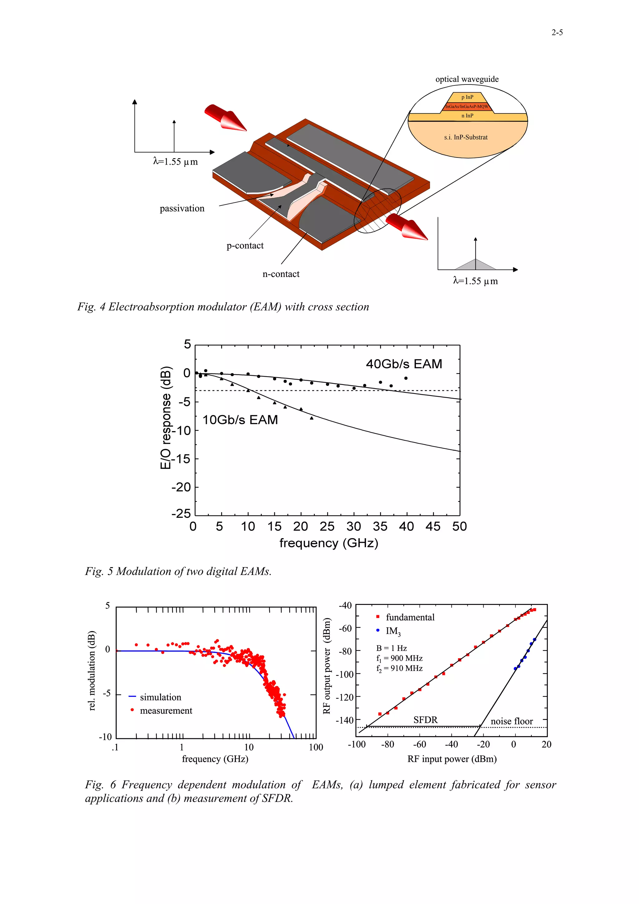
![2-6
3.2 Electroabsorption detector - Due to the electroabsorption mechanism, i. e. the
generation of charge carriers, the EAM can also be used as an – electro-absorptive -
photodetector (EAD). A bandwidth of >170 GHz is experimentally demonstrated (Fig. 7) for
a traveling-wave pin diode with an active multiple quantum well region. The traveling wave
design [14] again includes an optical waveguide and an electrical coplanar transmission line
along the optical signal path, see Fig. 3: In this case there is no optical output and no electrical
input. Experimentally, a heterodyne set-up has been used where two optical input signals with
a corresponding difference frequency are fed into the optical waveguide of the EAD. The
photodetection process leads to a photocurrent at the difference frequency measured after
down-conversion with a spectrum analyser.
0
10
0
0
output power (dBm)
-10
-20
-30
-40
25 50 75 100 125 150 175 200
frequency(GHz)
Fig. 7 Frequency response of a traveling-wave 1.55µm photodiode using electroabsorption in the
MQW active material of the optical waveguide
Recently, a traveling wave photodetector has been shown to work up to 460 GHz as
measured using an SIS mixer (a superconducting Josephson junction) in a THz-antenna
system for radio astronomy [15]. Here the photodetector together with the two laser diodes
work as a photonic local oscillator
3.3 Electroabsorption mixer - Due to the inherent nonlinearity of the photodetector where
the photocurrent is proportional to the square of the electric field of the optical wave, this
electroabsorptive device can further directly be employed as a photomixer (EAX).
Experimental results for up-conversion at 60 GHz are shown in Fig. 8. In this experiment,
again a heterodyne set-up has been used where the two laser diode signals are separated by 60
GHz and one laser diode is additionally modulated at 2.6 GHz. Obviously, the electrical
output signal exhibits the RF carrier frequency as well as the side bands due to modulation.](https://image.slidesharecdn.com/en-028-all-120926115440-phpapp01/75/En-028-all-52-2048.jpg)
![2-7
- 20
upconverted downlink sign (dBm)
- 40
- 60
- 80
54 56 58 60
frequency (GHz)
Fig. 8 Optoelectronic mixing in a photodetector, here an electroabsorption photomixer (EAX)
3.4 Electroabsorption transceiver – From the physics of electroabsorption it is concluded
that the EAM can simultaneously be used as a modulator and a photodetector where for
communication techniques the electrical up- and downlink signals of the device have to be
frequency multiplexed. Such a dual function EAM is called electroabsorption transceiver
(EAT), [16], Fig. 9. The multifunctional characteristics of such an EAT are finally
demonstrated in different fiber wireless systems for broadband communications, see below.
bias voltage (V)
-2 -4 -6 -8
0 1.2
transmission (dB)
sensitivity (A/W)
sensitivity (A/W)
-10 λ=1.55µm 0.8
λ=1.51µm
-20 0.4
-30 0
0 -1 -2 -3 -4
bias voltage (V)
Fig. 9 Photodetection and modulation properties of an electroabsorption modulator. The device is
called an electroabsorption transceiver (EAT)
3.5 Electroabsorption SEED element - An EAT can further be used to generate artificial
optical nonlinearities such as optical bistability [17] which gives rise to switching, logic and
memory effects. From the physical point of view this nonlinearity is caused by the internal
feedback between the modulator and the photodetector properties of the device. It has been
shown that this characteristic nonlinearity may be useful for multiple-GHz A/D conversion.](https://image.slidesharecdn.com/en-028-all-120926115440-phpapp01/75/En-028-all-53-2048.jpg)
![2-8
3.6 Microwave laser diodes - Up to now laser diodes are usually not made using a special
design for microwave applications [18]. In particular, no traveling wave structures are applied
although the electrical contact size is already close to the electrical wavelength for
frequencies of about 10 GHz. As a result, since several years the cut-off frequency is only
about 30 GHz and there is no breakthrough at higher frequencies.
4. OPTOELECTRONIC INTEGRATION TECHNOLOGIES
In an optoelectronic TW device [7,8,9] an optical waveguide (e. g. a strip loaded or a
burried waveguide) is used for optical wave propagation and an electrical transmission line (e.
g. microstrip or coplanar waveguide) for guiding the microwave, usually in the same
direction. In the region where the electrical fields overlap, the optoelectronic interaction
occurs. Note that a dc bias may additionally be applied to control the operating point. From a
physical point of view the interaction is a nonlinear or active process. As discussed above, the
photodetector and the laser diode are basic examples of two-port devices where optical power
is converted into electrical power and vice versa. Typical three-port devices are electrically
controlled optical modulators/switches or optically controlled microwave modulators/-
switches. Due to the inherent nonlinearity these devices are further used for optoelectronic
mixing of input electrical and/or optical signals where the output signal can be electrical or
optical. As a result, such microwave optical interaction devices show a variety of
optoelectronic functions where in special devices different functions may be achieved
simultaneously.
A novel multifunctional device has recently been presented, the electroabsorption
modulator integrated into the structure of a hetero-bipolar transistor (HBT), [19]. Such a
device (Fig. 10) includes the common transistor characteristics as well as the modulator
behaviour leading to a novel approach to optoelectronic integrated devices and circuits.
Fig. 10 SEM picture of an HBT-EAM
A further key integration technology is the optical coupling of the light between the
optical waveguide and the external connection which usually is the optical fiber. This
technique of fiber chip coupling includes the processing of V-grooves into the substrate or](https://image.slidesharecdn.com/en-028-all-120926115440-phpapp01/75/En-028-all-54-2048.jpg)
![2-9
mother board and the tapering of the optical fiber [20] A further important technology is
related to the adjustment and fixing of the fiber with respect to the optical waveguide. A result
of measurement is shown in Fig. 11 where a coupling loss of less than 1 dB is achieved for a
MFD of about 1.5 µm. It should finally be mentioned that high frequency electrical coupling
of coplanar lines with coaxial connectors requires also a careful design of wire bonding.
8
coupling efficiency (%)
20
coupling loss (dB)
6
4
50
measured
2
calculated
0 100
0 2 4 6 8 10
MFD (µm)
Fig. 11 Fiber chip coupling: coupling loss versus mode field diameter (MFD)
5. PHOTONIC MICROWAVE SIGNAL PROCESSING
In the following a few examples of optically controlled microwave devices and modules
are discussed. The physical mechanisms are due to the optical generation of free charge
carriers in a semiconductor leading to a control of some key electrical parameters determining
the microwave properties.
5.1 Photonic microwave phase shifter/time delay control - In Fig. 12 electrical trans-
mission lines- microstrip and coplanar – are sketched where the strip or the center conductor
metal forms a Schottky contact with the semiconductor [6,7]. As a result the high capacitance
per unit length gives rise to a slow mode behaviour and the electrical wavelength or the phase
velocity are given by the width of the depletion region of the contact. This thickness of the
space charge region furtheron depends critically on the applied reverse bias voltage (electrical
control of the phase velocity and the delay time). When a fixed bias voltage is applied using
an external series resistor, the voltage drop across the depletion layer can also be changed by
absorption of an optical signal in the space charge region. As a result, the time delay is
controlled optically and because it is a usual transmission line a true time delay shift occurs.
V0 V0
(a) (b)
Fig. 12 Optically controlled phase shifter and time delay control using a Schottky contact
microstrip line](https://image.slidesharecdn.com/en-028-all-120926115440-phpapp01/75/En-028-all-55-2048.jpg)
![2-10
5.2 Photonic ultrawide band (UWB) pulse generation - Fig. 13 elucidates an optically
controlled generation of microwave pulses. The structure consists of a stripline resonator in
the center with two gaps on each side. On the left hand side a dc or RF source is connected
charging the resonator. On the right hand side an optoelectronic switch (OES) – the second
gap - is provided which can optically be switched on in order to connect the output port of the
resonator directly to an integrated antenna. Two operating scenarios can be distinguished: (i)
Using a dc source the resonator is charged and by closing the OES a pulse is generated
traveling to the antenna. The temporal width of the pulse is given by the length of the
resonator (frozen wave generator). Please note that specific pulse forms are generated given
by the structure of the charge line. (ii) Using a RF source the resonator is also charged and a
standing wave of large amplitude, depending on the quality factor of the transmission line, is
established. When the OES is optically closed, the standing wave will become a propagating
wave and a short ultra broadband (UWB) pulse is generated and radiated using, for example, a
broadband slot antenna [21,22]. This technique is a kind of pulse compression [23] known
from nonlinear optics and soliton theory.
DC
light
Fig. 13 Optoelectronic switching of a microwave resonator to obtain UWB signals
5.3 RF spectrum analyser - By using the techniques of 5.1 and 5.2 in an 2-dim or even 3-
dim array parallel microwave signal processing becomes possible. Fig. 14 shows a microwave
circuit where the input signal is divided into several channels and where each channel
contains a time delay (T) and an amplitude (a) control using optical techniques as above
mentioned. When the output signals are finally combined to a common connection a
transversal filter results. In contrast, when the individual channels would be connected to
antennas, a phased array antenna system results.](https://image.slidesharecdn.com/en-028-all-120926115440-phpapp01/75/En-028-all-56-2048.jpg)
![2-11
Popt
T1 a1
T2 a2 filter
. .
. .
. .
. .
. .
. .
. .
. .
Ti ai
phased array
Fig. 14 Microwave signal processor
6. BROADBAND FIBER OPTICAL LINKS
An analog or digital - optical link consists of an optical transmission medium (preferably
a fiber) and optoelectronic converters on both sides, see Fig. 15. The great advantage of such
an optical link is that due to the broadband low-loss transmission capability the optical fiber
(see Fig. 15) can ideally be used to transmit microwave signals and therefore replace other
lossy metallic waveguides, see Fig. 16. Here different techniques have been explored. For
example, on the transmitting side a cw laserdiode and an external modulator (electrooptic or
EAM) and on the receiving side an optoelectronic photodetector can be used. Besides the
bandwidth a key parameter of such a link is the link loss which depends on the conversion
efficiencies of the optoelectronic elements, the optical coupling efficiencies and the
attenuation and dispersion of the transmission medium [24]. Note that a link gain can easily
be achieved when an optical amplifier (EDFA) and/or external modulators, preferably on both
sides, are being used [24]. For high-speed and broadband operation the a. m. TW microwave
photonic devices can succesfully be employed.
e o
o e
optical fiber
(free space)
Fig. 15 Optical interconnection replacing an electrical cable](https://image.slidesharecdn.com/en-028-all-120926115440-phpapp01/75/En-028-all-57-2048.jpg)
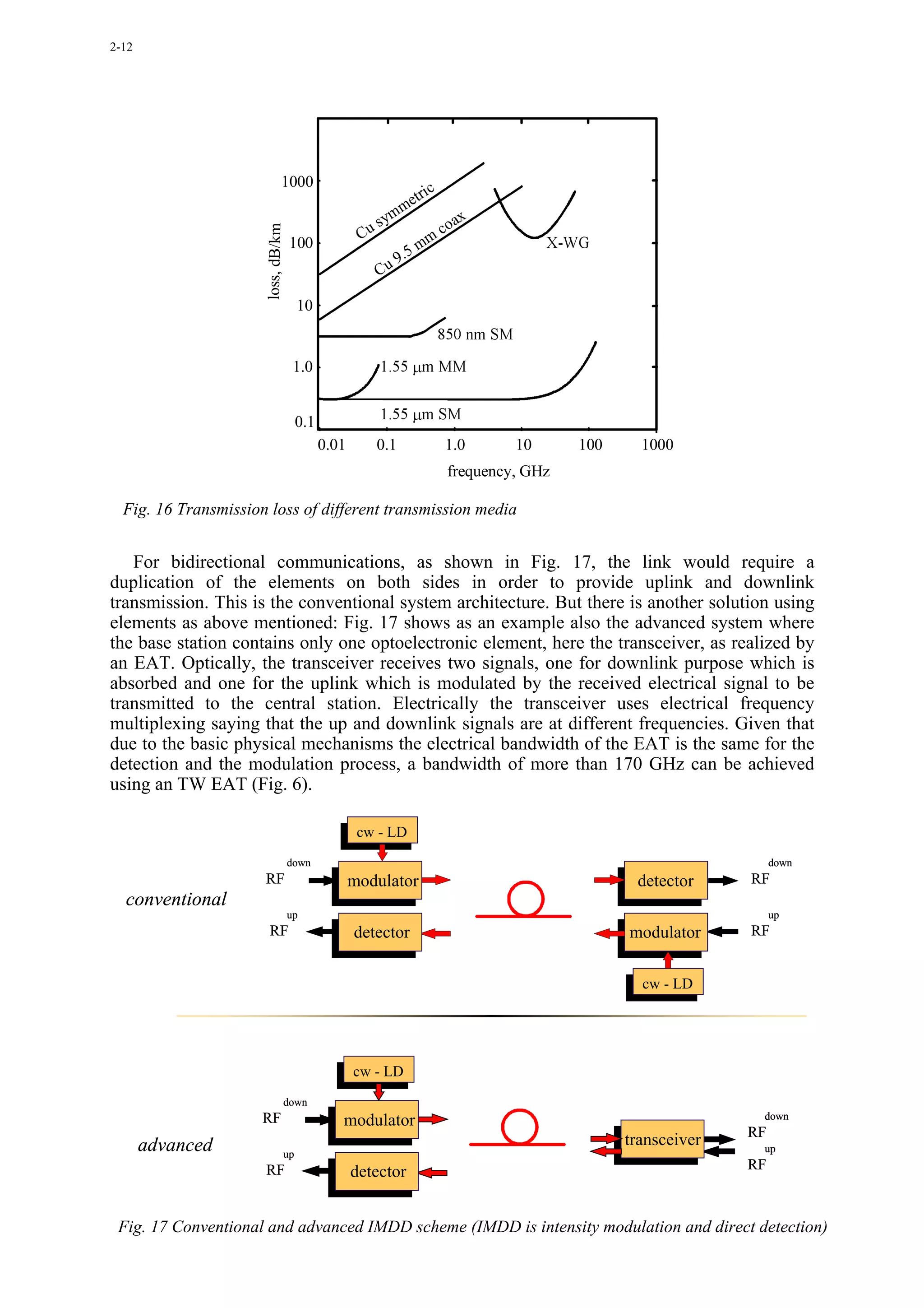
![2-13
7. MICROWAVE PHOTONIC SYSTEMS
Broadband fiber optic links are regarded to be basic building blocks for different
microwave systems where specific advantages of the optical interconnections and optical
signal processing capabilities are utilized. A few areas of significant applications are reviewed
in the following.
7.1 Photonic local oscillators - Transmitting two optical wavelengths by using two frequency
locked lasers or a two mode laser and mixing the two optical signals in a photodetector/-mixer
emulates a microwave local oscillator where the difference frequency is photonically
generated by heterodyne techniques and where wavelength tuning provides a bandwidth of
several THz depending on the bandwidth of the detector [25]. Note also that an optically
induced phase shift is directly transferred into the electrical domain. Fig. 18 shows a module
fabricated for radioastronomical antennas; the module consists of a traveling-wave
photomixer connected to a dc bias circuit with appropriate filters, a slot line antenna and a
quasi optical lens to focus the radiated beam at 460 GHz into an He cooled SIS mixer.
Fig. 18 Photograph of a photonic local oscillator module
7.2 EMC sensor - When the modulator at the end of a fiber is driven by an electrical input
signal at the given position, the received optical signal can be used to measure the electrical
signal quantitatively at the transmitter side and a field sensor results. Fig. 19 shows the circuit
diagramme of such an E-field sensor for EMC applications. The sensor head consists of a
dipole antenna. The output signal is fed into a transimpedance amplifier driving an EAM. The
optical input signal at 1.55 µm is delivered by a laserdiode in the remote unit which contains
also the photodiode to measure the output signal from the EAM in the sensor head. The dc
bias for the amplifier as well as for the operating point of the EAM is provided by a
photovoltaic cell (PVC) in the sensor head. A second laser diode in the read-out unit generates
the necessary optical power.](https://image.slidesharecdn.com/en-028-all-120926115440-phpapp01/75/En-028-all-59-2048.jpg)
![2-14
laserdiode λ=840 nm
(energy) PVC-array
laserdiode λ=1.55 µm planarer
(signal) Monopol
electroabsorption
modulator
transimpedence
transimpedence
amplifier
amplifier
interface
photodiode
Fig. 19 EMC sensor [26,27]
7.3 Electrooptic sampling and optoelectronic testing - Using electrooptical properties of a
semiconductor substrate (Fig. 20) an incoming optical beam is modulated by an applied
electrical field and the reflected optical signal can be used to determine the electrical field at
the position of the interaction. This set-up can directly be used to measure electrical fields,
e.g. in integrated circuits, with high spatial resolution (2-dim field mapping, [28,29]) and
without any mechanical contact. Moreover, characteristic sampling techniques have been
presented where optical pulses in the pico- or femtosecond range are applied giving a
measurement bandwidth in excess of 100 GHz. In a recently presented sensor, a
microminiaturized modulator chip working in reflection mode and coupled to the end of a
fiber has been applied to measure electrical fields in free space, again with high spatial
resolution. Such a fiber sensor is used for contactless high-speed testing of integrated circuits
or antenna radiation patterns [13] similarly to the EMC sensor mentioned before.
GaAs, InP
Laser beam
Fig. 20 Principle of electrooptic sampling](https://image.slidesharecdn.com/en-028-all-120926115440-phpapp01/75/En-028-all-60-2048.jpg)
![2-15
7.4 Hybrid fiber-coax (HFC) systems - In cable TV (CATV) techniques the RF signals
received from TV satellites are converted into the optical domain and fed into a fiber to be
transmitted over long distances with only small attenuation. The received optical signals are
converted back into the electrical domain and guided to the costumer via coaxial cable. This
HFC technique using again the advantages of the optical fiber transmission is continuously
installed in major cities around the world where the uni-directional technique is replaced more
and more by bi-directional links in order to establish a back channel, e. g. for multimedia
applications.
7.5 Fiber-radio systems - It is agreed that fiber-radio access will provide a solution to the
demands for a wireless connection to the costumer (“last or first mile problem”). For
broadband services the frequencies are in the millimeterwave range, for example at 40 GHz or
60 GHz. Such a concept is based upon an optical link between the central office and the base
stations in a picocellular structure which results from the high free space attenuation of the
millimeterwave signal. As an example, 60 GHz fiber radio links have been demonstrated
providing 155 Mbps and using EAMs for half-duplex and EATs for full-duplex transmission
in a WDM ring network [30-32]. It is foreseen that for next generation broadband photonic
communication networks, the electroabsorption modulator (EAM) and the electroabsorption
transceiver (EAT) will be key elements. Experimentally, full duplex transmission in a WDM
ring network and electrical frequency division multiplex (EFDM), as sketched in Fig. 21,
have been studied. Here two CW LDs at different wavelengths are used to drive the
modulator function of the EAT in each base station (BS) addressed by the optical wavelength
(WDM technique). The other two LDs are externally modulated in the central station (CS) to
provide the downlink transmission. These signals are absorbed in the EATs of the base
stations to feed the wireless link. The electrical FDM technique is obvious from Fig. 17:
downlink and uplink RF frequencies are 59.6 GHz and 60 GHz, respectively. The
transmission quality at a data rate of 156 Mbps is finally determined and evaluated by a bit
error rate tester (BERT).
λ= 1580nm SMF
LD U1
DPSK
λ=1570nm 59.6GHz
LD U2 λ W-EDFA (demod .) BERT
(2.6 GHz)
O
E
M A
λ= 1540nm
A LO, 57GHz
U D
LD D2 EAM T
X M
DPSK
λ= 1530nm
60GHz PRBS
LD D1 EAM Att. (mod.)
(156 Mbps )
(3.0 GHz)
(BS)
59.6GHz
DPSK (MT)
PRBS (mod.)
(156 Mbps ) (2.6 GHz)
PD
DPSK
LO, 57GHz λ 59.6GHz (demod .) BERT
(2.6 GHz)
amplifier D O
DPSK E
E A
BERT (demod .) SMF A LO, 57GHz
M D
(3.0 GHz) 60GHz T
U M
X DPSK
60GHz PRBS
L-EDFA Att. (mod.)
(156 Mbps )
(3.0 GHz)
(CS) (BS)
(MT)
Fig. 21 Full-duplex 60 GHz mm-wave fiber wireless network employing an electroabsorption
transceiver (EAT) as a key photonic component in the base station (BS)
7.6 Antenna systems – A major application of optical link technology is the remoting of
antenna systems and, particularly, the optical control of array antennas, see for example](https://image.slidesharecdn.com/en-028-all-120926115440-phpapp01/75/En-028-all-61-2048.jpg)
![2-16
Refs. [33] and [34]. In the receiving mode a millimeterwave camera with photonic
interconnection is obtained. Different applications in imaging are foreseen.
8. CONCLUSIONS
In the past decade the field of microwave and millimeterwave photonics has become a key
technology extending from components and modules to systems with important applications
The driver has been twofold: On one hand the broadband low-loss and high-speed transmision
capability of optical fibers has led to a considerable interest in their use for distributing and
controlling micro- and millimeterwave signals. On the other hand the breakthrough in the
design and demonstration of several ultra-broadband photonic components has paved the way
for wideband and high efficiency optoelectronic converters being important building blocks
for microwave optical links. As a result, it can be foreseen that this multidisciplinary field of
microwave photonics will continously be expanded and lead to further novel concepts due to
the synergetic merging of different technologies.
In this contribution specific high-speed and broadband photonic components based upon
the physics of electroabsorption have been discussed. In particular, electroabsorption
modulators, photodetectors, mixers and transceivers have been presented. The
multifunctional properties of the transceiver elements have been proven to be especially
interesting. The performance of these elements has been demonstrated for example in a fiber-
wireless WDM ring network by BER measurements; but the advantages will generally hold
for other optical links with bi-directional transmission properties as well. The great advantage
of this concept is that in the base station (in the sensor head or at the antenna side) just a
single photonic component serves simultaneously as a converter for downlink and uplink
communication and information transport. It is therefore concluded that these elements may
play a significant and key role in fiber coupled wireless microwave and mm-wave networks
and for high date rate transmission services such as in multimedia techniques.
Acknowledgement – The authors wish to thank Professor K. Kitayama, Osaka University
and T. Kuri, Communications Research Laboratory, Tokyo, for their contribution to this work.
REFERENCES
[1] D. Jäger, “Traveling-Wave Optoelectronic Devices for Microwave and Optical Applications”,
1991, Proc. of Progress in Electromagnetics Research Symposium (PIERS), p. 327,
[2] D. Jäger, “Microwave Photonics”, in “Optical Information Technology”, S.D. Smith and R.F.
Neale (eds.), Springer Press 1993, pp. 328-333
[3] D. Polifko and H. Ogawa, “The Merging of Photonic and Microwave Technologies”, Microwave
Journal March 1992, pp. 75-80
[4] “International Topical Meeting on Microwave Photonics”, Techn. Digest, Kyoto 1996, Duisburg
1997, Princeton 1998, Melbourne 1999, Oxford 2000, Long Beach 2001
[5] IEEE Trans. Microwave Theory and Techn., Special Issues on Microwave and Millimeterwave
Photonics, Sept. 1995, Sept. 1997, July 1999, June 2001
[6] D. Jäger, “Characteristics of traveling waves along nonlinear transmission lines for monolithic
integrated circuits”, 1985, Int. J. Electron., vol. 58, pp. 649-669
[7] D. Jäger, R. Kremer, and A. Stöhr, “Traveling wave optoelectronic devices for microwave
applications,” 1995, IEEE Int. Microw. Symp. Digest, vol. 1, pp 163-166](https://image.slidesharecdn.com/en-028-all-120926115440-phpapp01/75/En-028-all-62-2048.jpg)
![2-17
[8] D. Jäger, R. Kremer, A. Stöhr, “High-Speed Traveling-Wave Photodetectors, Modulators and
Switches”, 1995 IEEE/LEOS Summer Topical Meeting, Keystone, USA, pp. 23-24, 1995. D.
Jäger, R. Kremer, “Traveling-Wave Optoelectronic Devices for Microwave Applications”,
Topical Meeting on Optical Microwave Interactions, pp. 11-14, 1994.
[9] D. Jäger, R. Kremer, O. Humbach, and A. Stöhr, “Traveling-Wave Optoelectronic Devices for
Microwave Photonics”, Emerging Optoelectronic Technologies, Conference Proceedings, Editors:
A. Selvarajay, B.S. Sonde, K. Shenai, and V.K. Tripathi, ISBN: 0-07-462397-4, pp. 409-413,
Bangalore, July 1994, (invited paper).
[10] T.H. Wood, “Multiple Quantum Wells (MQW) Waveguide Modulators”, J. Lightwave Technol.,
no. 6, p. 743, 1988.
[11] O. Humbach, A. Stöhr, U. Auer, E.C. Larkins, J.D. Ralston, and D. Jäger, “Strained-Layer
Multiple Quantum Well InGaAs/GaAs Waveguide Modulators Operating at 1µm”, IEEE
Photonics Technology Letters, vol. 5, no. 1, pp. 49-52, January 1993.
[12] A. Stöhr, O. Humbach, S. Zumkley, G. Wingen, G. David, B. Bollig, E.C. Larkins, J.D. Ralston,
and D. Jäger, “InGaAs/GaAs Multiple Quantum Well Modulators and Switches”, Optical and
Quantum Electronics, vol. 25, pp. 865-883, August 1993, (invited paper).
[13] N. Mineo, K. Nagai, T. Ushikubo, “Ultra-Wideband Electro-Absorption Modulator Modules for
DC to Millimeter-Wave Band”, Topical Meeting on Microwave Photonics, pp. 9-12, Jan. 2002.
[14] A. Stöhr, R. Heinzelmann, A. Malcoci, and D. Jäger, “Optical Heterodyne Millimeter-Wave
Generation Using 1.55µm Traveling-Wave Photodetectors,” IEEE Transactions on Microwave
Theory and Techniques, vol. 49, no. 10, part. 2, pp. 1926-1933, October 2001.
[15] A. Stöhr, A. Malcoci, F. Siebe, K. Lill, P. van der Waal, R. Güsten, and D. Jäger, “Integrated
Photonic THz Transmitter Employing Ultra-Broadband Traveling-Wave 1.55µm Photodetectors”,
Int. Topical Meet. on Microwave Photonics, MWP 2002, (submitted).
[16] A. Stöhr, R. Heinzelmann, T. Alder, and D. Jäger, “Electroabsorption Transceiver (EAT) for
Fiber-Wireless Networks,” International Topical Workshop on Contemporary Photonic
Technologies 2000 (CPT’2000), Tokyo, January 2000.
[17] D. Jäger, “Large optical nonlinearities in hybrid semiconductor devices”, J. Opt. Soc. Am. B/vol.
6, pp.588-594
[18] D. Tauber et al., “The Microstrip Laser Diode”, Phot. Techn. Lett. vol. 10, no. 4, pp. 478-480
(1998)
[19] M. Schneider, T. Reimann, R. Heinzelmann, A. Stöhr, P. Velling, S. Neumann, R. M. Bertenburg,
F.-J. Tegude, and D. Jäger, “A novel 1.55 µm HBT-Electroabsorption modulator,” Tech. Digest,
2001 Int. Top. Meeting Microw. Phot. MWP `01, Long Beach, Jan. 2002
[20] T. Alder, A. Sröhr, R. Heinzelmann, and D. Jäger, “High Efficient Fiber-to-Chip Coupling Using
Low-Loss Taperewd Single Mode Fiber,” IEEE Photon. Techn. Lett., vol. 12, no. 8, pp. 1016-
1018, 2000
[21] R. Heidemann, Th. Pfeiffer, and D. Jäger, “Optoelectronically pulsed slot line antennas,”
Electron. Lett. Vol. 19, pp. 316-317, 1983
[22] P. Paulus, W. Brinker, and D. Jäger, “Generation of microwave pulses by optoelectronically
switched resonators”, IEEE J. Quantum Elecgtron. Vol. QE-22, pp. 108-111, 1986
[23] P. Paulus, L. Stoll, and D. Jäger, “Optoelectronic pulse compression of microwave signals”, IEEE
Trans. Microw. Theory Techn., vol. MTT-35, pp. 1014-1018, 1987
[24] D. Jäger, “Advanced microwave photonic devices for analog optical links”, 1998, Int. Top.
Meeting on Microwave Photonics Digest, Princeton, pp.
[25] A. Stöhr, R. Heinzelmann, K. Hagedorn, R. Güsten, F. Schäfer, F. Siebe, H. Stüer, P. van der
Waal, V. Krozer, M. Feiginov, D. Jäger, “Integrated 460GHz Photonic Local Oscillator,”
Electron. Lett., vol. 37, no. 22, pp. 1347-1348, Oct. 2001.
[26] R. Heinzelmann, A. Stöhr, M. Groß, D. Kalinowski, T. Alder, M. Schmidt, and D. Jäger,
“Optically powered remote optical field sensor system using an electrabsorption modulator”,
1998, IEEE Int Microw. Symp. Digest, pp. 1225-1228
[27] A. Stöhr, R. Heinzelmann, R. Buß, and D. Jäger, “Electroabsorption Modulators for Broadband
Fiber Electro-Optic Field Sensors”, in Applications of Photonic Technology 2, Eds. G.A.
Lampropoulos and R.A. Lessard, Plenum Press, New York, pp. 871-876, ISBN 0-306-45808-X,
August 1996.](https://image.slidesharecdn.com/en-028-all-120926115440-phpapp01/75/En-028-all-63-2048.jpg)
![2-18
[28] G. David, R. Tempel, I. Wolff, and D. Jäger, “Analysis of Microwave Propagation Effects using
2D Electro-Optic Field Mapping techniques,” Optical Quantum Electron. Special Issue, pp. 919-
931, 1996
[29] G. David, P. Bussek, U. Auer, F.-J. Tegude, and D. Jäger, “Electro-Optic Probing of RF-Signals
in Sub-µm MMIC-Devices,” Electron. Lett., vol. 31, no. 25, pp. 2188-2189, 1995
[30] K. Kitayama, A. Stöhr, T. Kuri, R. Heinzelmann, D. Jäger, and Y. Takahashi, “An approach to
single optical component antenna base stations for broadband millimeterwave fiber-radio access
systems,” IEEE Trans. Microw. Th. Techn, vol 48, no. 12, pp 2588-259, December 2000.
[31] K. Kitayama, T. Kuri, R. Heinzelmann, A. Stöhr, D. Jäger, and Y. Takahashi, “A Good Prospect
for Broadband Millimeter-Wave Fiber-Radio Access System - An Approach to Single Optical
Component at Antenna Base Station,” in IEEE MTT-S International Microwave Symposium and
Exhibition, pp. 1745-1748, Boston, June 2000.
[32] Stöhr, K. Kitayama, and D. Jäger, “Full-Duplex Fiber-Optic RF Subcarrier Transmission using a
Dual-Function Modulator/Photodetector”, IEEE Transactions on Microwave Theory and
Techniques, vol. 47, no. 7, pp. 1338- 1341, July 1999.
[33] M. Y. Frankel and R. D. Esman, “True Time-Delay Fiber-Optic Control of an Ultrawideband
Array Transmitter/Receiver with Multibeam Capability”, IEEE Trans. Microwave Theory Techn.
vol. MTT-43, no. 9, pp. 2387-2394, September 1995
[34] P. J. Matthews, P.-L. Liu, J. B. Medberry, M. Y. Frankel, and R. D. Esman, “Demonstration of a
Wide-Band Fiber-Optic Nulling System for Array Antennas”, IEEE Trans. Microwave Theory
Techn. vol. MTT-47, no. 7, pp. 1327-1331, July 1999.](https://image.slidesharecdn.com/en-028-all-120926115440-phpapp01/75/En-028-all-64-2048.jpg)
![Click here to view slide presentation presented in PDF format 3-1
Wireless and Optics – A Survey and Overview of
Broad Band Fiber-Fed Radio Systems
J. J. Lee
Raytheon Electronics Systems
R2-V518 PO Box 902, El Segundo CA 90245, USA
jjlee8@west.raytheon.com
Abstract – This paper was prepared for NATO’s RTA Lecture Series No. 229
presented at the workshop of Optics-Microwave Interactions held in September 2002.
This lecture reviews recent developments of fiber-fed radio systems, an emerging
technology using fiber optic networks to distribute broad band RF and MMW signals
for mobile and wireless systems over long distance and within small cells.
------
This lecture note is a supplement to the vugraphs package (see attachment)
presented at the workshop. Basically, it is a condensed version of the text portion
(annotation) attached to the vugraphs (Power Point charts).
What is “Fiber Radio?” Fiber Radio is a fiber-fed radio system using fiber optic links or
networks to distribute video, voice, and data for mobile and wireless applications.
Antenna remoting is an example where MMW subcarriers at 18, 24, 38, or 60 GHz
with information are transmitted from central office to base stations. This emerging
technology has been demonstrated for applications such as community
communications and pico-cell wireless systems for both uplinks and downlinks
broadcast carrying CATV, WLAN signals and data ranging from 2 to 156 Mbps.
According to a McKinsey report, August 2001, the market trend for this industry is
hard to predict at this point. In general, the telecom markets have slumped for the last
few years. The slowdown was caused by over-capacity and unrealistic forecast.
Numerous start-ups were funded five years ago, but many stocks dropped by 80
percent or more in value since then. Many US companies have suffered great losses.
However, the demand for broad band services is for sure increasing. It is estimated
that the growth rate may reach 25 percent a year. Thus the over-capacity or glut may
be absorbed in a few years. It can be safely remarked that the “fiber-radio” technology
is attractive, but it is not a huge mature market yet.
1. Applications of Fiber-Radio Systems
Several fiber-radio system architectures have been studied and demonstrated. A
typical infrastructure concept was reported by Wake, et al [Optical Generation of
MMW Signals … in IEEE Trans. MTT, p.2270, 1995]. He described a system where
an optical fiber system with optical couplers (splitter) was used to distribute radio
signals with MMW subcarriers broadcast over many pico-cells (200 m range) for
community services.
Paper presented at the RTO SET Lecture Series on "Optics Microwave Interactions", held in
Jouy en Josas, France, 2-3 September 2002; Duisburg, Germany, 5-6 September 2002;
Budapest, Hungary, 9-10 September 2002, and published in RTO-EN-028.](https://image.slidesharecdn.com/en-028-all-120926115440-phpapp01/75/En-028-all-65-2048.jpg)
![3-2
More details of similar system concepts were provided by Ogawa el al [MMW Fiber
Optic Systems for Personal Radio Communications, IEEE Trans. MTT, p. 2285,
2002]. They studied and conducted an experiment reporting that excellent
performance of IF links with 70 MHz QPSK and 300 MHz FM on 26 GHz subcarriers
were obtained. For downlinks from central office to base stations, several modulation
schemes were discussed. For uplink from base stations to central office, low
frequency lasers and photodetectors could be utilized because data rate and traffics
were not as high as downlinks.
Han, Kim, and Chung at Korea Advanced Institute of Science and Technology studied
a multi-purpose fiber optic access network, where CATV, PCS, and base band signals
were multiplexed and carried by 10 km optical fibers to various nodes for distribution.
They presented the RF performance of various services with geographical and
technical specifications.
Ahmed, et al [37-GHz Fiber-Wireless System for Distribution of Broad Band Signals,
IEEE, MTT, p. 1431, 1997] conducted an experiment using 36 GHz carriers to
broadcast audio, video, and CATV signals over short distance, establishing the
feasibility of fiber-radio links for wireless systems.
Fiber-fed radio systems can also be used to study the geographic arrangement of
base stations for optimum reception. Arrendonda, et al [Techniques for Improving In-
Building Radio Coverage Using Fiber-Fed Distribution Antenna Networks, IEEE AP-S
Symp, p. 1540, 1996] conducted a statistical study on diversity, placement, and
number of antennas in a fast fading Rayleigh environment for performance
improvement. They compared systems and data characteristics at 900 MHz, 1.8 and
1.9 GHz, and found that multiple distributed antennas improved coverage, reduced
dynamic range required, and eliminated deep fades.
Fiber-fed radio systems may include a photonic network to distribute local oscillator
signals. High frequency channels with external modulators and low frequency
channels with direct modulators can be combined and distributed through the optical
fiber system for various mixing and conversion functions. Photonics will be a key
technology to reduce the size and weight of a complex LO distribution system for
broadcast, multicast, or point to point connections.
2. Components of Fiber-Radio Systems
Several charts are included to cover the components of the fiber-fed radio systems,
including MMW sources, transmitters, modulators, WDM, couplers, amplifiers, and
detectors.
To be reviewed first are the schemes and performance issues of antenna remoting
using direct and external modulators in the photonic links. The talk will discuss how to
improve link performance with increase of laser power and photodetector output
current in a link with external modulator for MMW subcarriers distribution.](https://image.slidesharecdn.com/en-028-all-120926115440-phpapp01/75/En-028-all-66-2048.jpg)
![3-3
To overcome the difficulty in producing high quality MMW sources by conventional RF
means, one may consider optical generation by heterodyne methods (beating two
optical lines) or using mode-lock lasers. Vieira et al [A Mode-Locked Microchip Laser
Optical Transmitter for Fiber Radio, IEEE MTT, p. 1882, 2001] offered such a
solution.
At the output side of the link, extracting 60 GHz MMW signals with a photodetector is
not an easy task when efficiency, cost, and reliability are taken into account. One
example was given by Rohde el al [Optical-MMW Converter for 60 GHz Radio-over-
Fiber Systems.]
JDS Uniphase is one of the major companies developing key photonic components for
photonic and fiber-fed radio systems. A complete photonic network requires many
components, including laser sources, modulators, dense WDM, couplers (optical
splitters), amplifiers, optical switches, etc. Examples will be given to realize the
dimension and complexity of the key devices required for the system.
3. Issues and Performance Parameters of Fiber-Radio System
Several charts are provided to recognize the fact that the performance of a photonic or
fiber-fed radio system will be judged by the same set of parameters commonly used
and defined by the RF designers. These are gain, noise figure, signal to noise ratio,
dynamic range, bandwidth, third order intercept point, etc. Photonic links with COTS
(Commercially Off The Shelves) components for wide band and narrow band
requirements will be compared with a standard RF amplifier channel using typical wide
band COTS devices. It can be seen that it is still a challenging task to develop a
photonic link that can compete with a conventional RF channel using the same set of
performance parameters mentioned.
It can be summarized that fiber-radio is an emerging technology that will become more
attractive to distribute MMW broad band signals for wireless and mobile applications.
The demand for such systems is increasing for regional and community networks, but
so far no major venture capitals are rushing into the market yet. In other words, no
market “pain” or “killer application” has been identified to foresee a major shift in the
market trend for such products. Technology for laboratory demo is maturing, but lot
more product development is required to produce low cost and robust (reliable) MMW
and RF photonic components. In addition, it is necessary to further improve the
performance of fiber optic links for RF designers to accept and use photonics. There
are many photonic scientists, but it appears that engineering schools need to train
more students to become photonic system engineers.](https://image.slidesharecdn.com/en-028-all-120926115440-phpapp01/75/En-028-all-67-2048.jpg)

![Click here to view slide presentation presented in PDF format
4-1
RF Photonics for Beamforming and Array Applications
J. J. Lee
Raytheon Electronics Systems
R2-V518 PO Box 902, El Segundo CA 90245, USA
jjlee8@west.raytheon.com
Abstract – This paper was prepared for NATO’s RTA Lecture Series No. 229 presented
at the workshop of Optics-Microwave Interactions in September 2002. This lecture
focuses on the applications of RF photonics for array antennas in signal distribution,
beamforming, beam control, and antenna remoting. Examples are given to discuss the
requirements, benefits, and design approaches of photonics for phased array antennas.
The first demonstration of using photonics for a dual band array was conducted in 1990.
Later a wide band conformal array controlled by photonics was built and tested. This
example talks about the optical control of phased arrays by using fiber-optic links for RF
and data remoting and a time-shift beamforming network for wide instantaneous
bandwidth. Last, the talk will illustrate how photonics can be used to form a wide band
feed system for multibeam arrays.
1. Background
This lecture note is supplemented with a set of vugraphs (attachment), and these charts
are now summarized with the following annotations. Why RF photonics? There is
growing interest in applying photonic technology to phased arrays for signal distribution,
beamforming, and antenna remoting [1-6]. Recently, significant progress has been made
in the reduction of RF to optics conversion loss. As a result, antenna systems can benefit
in the areas of wide instantaneous bandwidth, immunity to EMI, lower transmission loss
for data remoting, and eventually reduction in size and weight as a goal.
Since 1980 Raytheon and HRL have been funded by DARPA and AFRL to demonstrate
several wide band arrays and feed networks using photonic technology. The concept of
wide band arrays centers on the usage of a true time delay beamforming network. A
large array is usually divided into many subarrays, with each subarray supported by a
programmable delay line. Within each subarray, phase shifters are used on the element
level, where 360 degree phase shift is provided to tilt the wave front for a given scan
angle.
The first dual band array (X- and L-band) was demonstrated in 1990. The L-band array
has 8 elements while the X-band array has 32 elements. Each array was divided into four
subarrays. A four-channel fiber optic true time delay feed network was built to scan the
beam for both frequency bands. The delay line is a 3-bit assembly consisting of a 1:8
divider with 8 lasers followed by eight fibers with different precut lengths. Scan
performance will be shown to illustrate that there is no beam squint (angular change)
when the frequency was switched from one band to the other by using the same set of
photonic delay lines for beam steering.
Paper presented at the RTO SET Lecture Series on "Optics Microwave Interactions", held in
Jouy en Josas, France, 2-3 September 2002; Duisburg, Germany, 5-6 September 2002;
Budapest, Hungary, 9-10 September 2002, and published in RTO-EN-028.](https://image.slidesharecdn.com/en-028-all-120926115440-phpapp01/75/En-028-all-69-2048.jpg)


![4-6
5. Multi-beam Photonic Array Feed
Photonics can also be used to support a multibeam wide band feed for array antennas.
The main advantage is to reduce the complexity of the array front end. This is
accomplished by replacing multiple sets of discrete phase shifters at the array element
level with a simplified fiber optic Rotman lens supplemented with a RF heterodyne
technique for fine scan. The feed “engine” can be used for both transmit and receive
operations. On receive, the signal across the aperture is conjugatedly matched at the
front end by a reverse phase gradient produced by the transmit network.
This development was motivated by the need to reduce the number of antennas on many
airborne and shipboard platforms. Conventional techniques to achieve multiband and
multibeam capabilities are impractical because of the size, weight, packaging density,
and high cost of the beamforming networks. Packaging is difficult because of the small
element spacing required for a typical 3:1 bandwidth array. It is a major challenge to
package multiple sets of phase shifters, drivers, and control lines in the space available
behind each element. Also, phase shifters are usually lossy, complex, and expensive to
fabricate. In addition, heat dissipation imposes a heavy burden on the mechanical and
thermal designs needed to achieve dense module packaging. Thus, innovative multibeam
feed and independent beam scan concepts are needed.
The new beamforming system uses a simplified Rotman lens configuration
supplemented with a RF heterodyne system to provide continuous scan. The
configuration consists of a few feed ports to point the beams in the general directions
over a ±60° range, and the heterodyne system scans the beam over a small region
around the discrete offset angles. This phase-locked RF mixing feed combines the signal
distribution and beam scan unit into one beamformer for both transmit and receive
operations, thereby replacing the multitude of phase shifters, drivers, and beam control
circuitry conventionally used. Heterodyne approaches had been studied before, but none
has focused on the aspect of wide band and multibeam applications [7-16].
The basic architecture of the multifunctional, wide band beamformer will be discussed,
using a 16-element array with five feed ports as an example. Each port covers a 30-
degree sector over the ±60° scan range in the azimuth plane. Within any sector, each
beam is steered by a heterodyne phase-locked loop, which constrains two frequencies ω1
and ω2 to produce a constant beat frequency, ω0, radiated by the linear array. Frequency
ω1 is fed into the constrained lens as a reference signal. To a first order approximation,
this signal provides a uniform amplitude and certain phase distribution across
16 elements along the pick-up side of the Rotman lens. The second frequency, ω2, from
an offset feed port supplies the desired phase gradient along the same 16 elements to
steer the beam in the desired direction when the phase front is transferred to the array
aperture. These two frequencies will mix to produce the constant ω0. However, the
spatial phase gradient is not affected by the heterodyne process. By varying ω2 and ω1 the
phase gradient along the aperture and, hence, the beam direction, can be changed. By
exciting other feed ports, one can use the same heterodyne process to generate multiple
beams with different pairs of RF frequencies.](https://image.slidesharecdn.com/en-028-all-120926115440-phpapp01/75/En-028-all-74-2048.jpg)
![4-7
Next, the issue of bandwidth and beam broadening is considered. It can be shown that,
to a first order approximation, the amount of beam squint normalized to its local
beamwidth for a given bandwidth ∆f 0 is given by
∆θ o N ∆fo d R f
= Sinθ R 1 − 2 (1)
BW 2 f MAX d o fo
where N is the number of elements, fMAX is the highest operating frequency of the
antenna, and fo is the current operating frequency. The element spacing is assumed to
be do = λMIN/2 where λMIN is the wavelength corresponding to fMAX. A criterion to define
the bandwidth is to restrict the squint (absolute value) to be less than one quarter or one
half of the beamwidth. So one can set
∆θ o N ∆fo d R f2
= Sinθ R 1 − <0.5 (2)
BW 2 f MAX d o fo
to calculate the maximum size of the array (N) for a given bandwidth (∆f o/f max) in terms of
feed angle θR, relative element spacings, and vice versa. Note that when f2 is equal to f0
without heterodyne, the system degenerates into a conventional Rotman lens with infinite
bandwidth, consistent with the definition of a true time delay beamformer. Also, when f2
is varied to go above or below fo the beam will deviate from the normal setting θo,
scanning to the right or left depending on the frequency variation. This is the basic
principle of the heterodyne beam scan system.
6. Fiber Optic Implementation
The space feed can be replaced by bundles of fibers precisely cut to produce perfect
wave fronts for the directions associated with the feed ports. The fiber version of the feed
makes the system compact and foldable. Using light sources of different colors will
provide high isolation between independent beams. A special case of the system was
described in [16], in which one set of equal-line-length fibers represents the central
reference port and another set of unequal-line-length fibers of incremental length ∆L
generates the phase gradient required to scan the beam by frequency control through a
phase-locked loop. Multibeam operation is achieved by using laser light of different colors
to carry control signals for each beam while sharing the same fiber feed system. This
sharing is made possible by the use of optical wavelength division multiplexers (WDMs),
which allow light signals of different wavelengths to be combined, passed through the
common feed system, then separated at the output to generate independent,
noninteracting beams.
The transmit (TX) manifold can be used for receive by producing a conjugate phase front
to mix with the incoming wave. The TX “engine” produces an outgoing wave with a
slightly offset ω0 to heterodyne with the receive signal by another set of mixers. The IF
outputs at the elements can then be added in phase with a summing network and sent to
the remote site by digital photonics for further filtering and processing. Again, multiple
beams can share the same beamforming manifold to reduce cost and complexity. The
receive signal does not go through the entire beamforming manifold in the reverse
direction. Hence, the overall noise figure is not degraded by the total loss of the
beamformer in the transmit path. This is especially significant when the photonic
conversion loss is still high. With the new design, the receive path bypasses most of the](https://image.slidesharecdn.com/en-028-all-120926115440-phpapp01/75/En-028-all-75-2048.jpg)


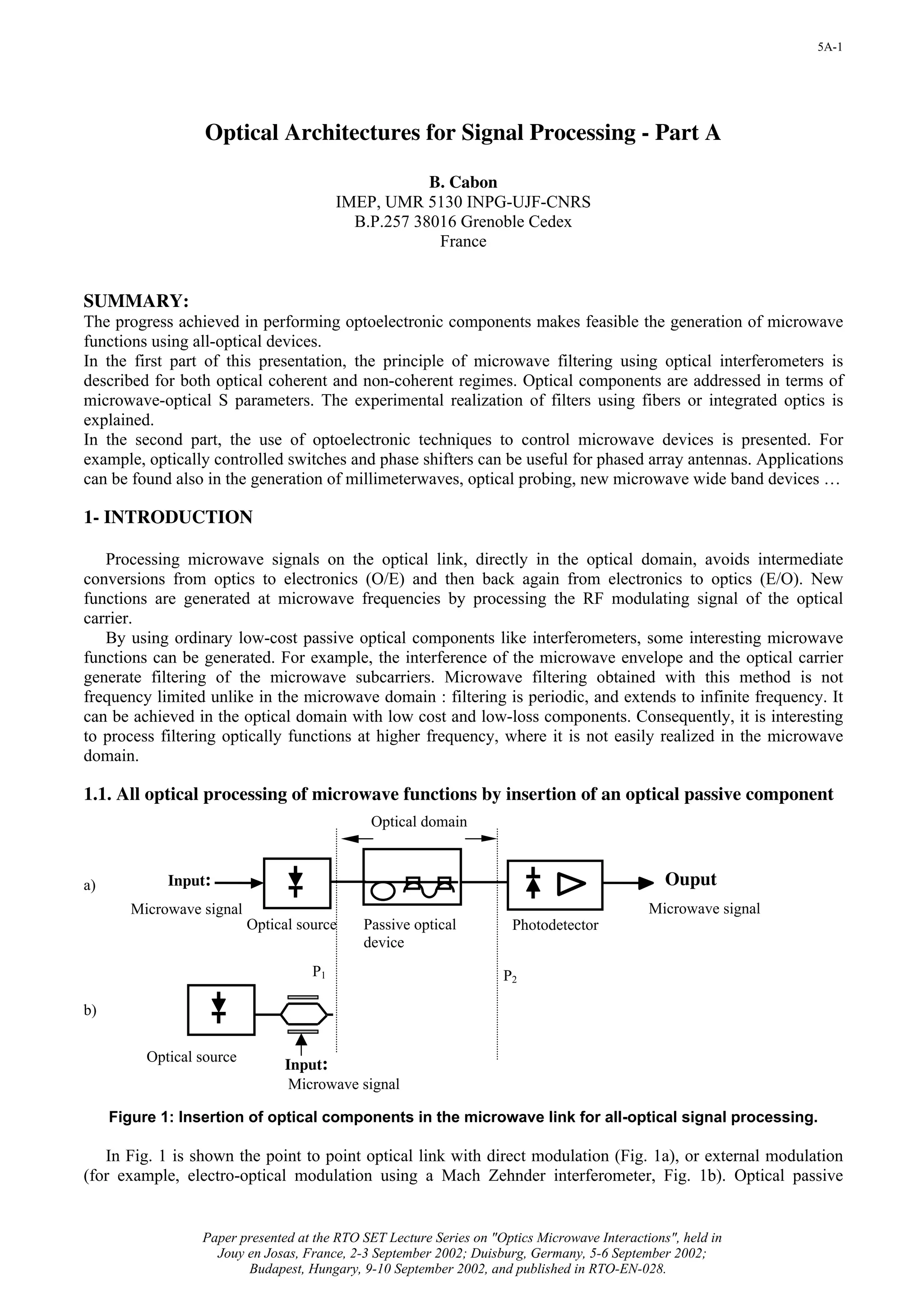
![5A-2
devices can be inserted between planes P1 and P2 for achieving optical processing of the microwave subcarrier.
A passive interferometer inserted there, and made either of fibers and couplers or integrated optical
waveguides, can realize microwave filtering. This solution is presented in section 2. In section 1.2, we discuss
the transfer function of the filter in terms of S parameters and their variations with frequency.
1.2. Measurement of the optoelectronic scattering parameters
We consider here the external modulation, where the optical intensity is modulated at a microwave
frequency (modulation index m).
It is convenient to define the optoelectronic S parameters as in microwave. The optical scattering waves (ai,
bi) at each port, i , of the optical device, related to modulated optical intensity (envelope of the carrier) are :
a i = I ai m cos(ω m t + ϕ ai ) and b j = I bj m cos(ω m t + ϕ bj ) , where ϕai is the phase of the microwave
envelope at port i, related to the incident wave a, and ϕbj relates to the emergent wave b. Iai is the incident
optical intensity at port i, Ibi the emergent optical intensity at this port.
The optoelectronic S parameters of the optical device can then be defined as :
b I bi
Sij, opt = i = exp j(ϕ bi − ϕ aj ) . (1)
aj I aj
These S parameters defined with the optical intensity can be measured with a microwave Vector Network
Analyzer and its lightwave extension (Fig. 2).
The intensity of the light emitted by a DFB laser source (1300 nm) is modulated at the microwave
frequency fm by a microwave source modulating a MZ external modulator (E/O conversion). At the output of
a rapid photodetector (O/E conversion), a synchronous detection is operated by the Vector Network Analyzer.
The photocurrent detected by the photodetector is compared to a reference signal. The optoelectronic S
parameters are then obtained. The microwave frequency response, the insertion loss, the group delay, etc. are
finally derived.
Assuming a linear operation of E/O and O/E converters, then the optoelectronic transfer function S21, opt (fm) of
the optical device in the planes P1-P2 can be obtained by measurements. A preliminary calibration is done,
then the E/O and O/E are extracted. The global transfer function Tglobal is then measured in the reference
planes P3-P4 and then, the final transfer function requested in the reference planes P1-P2 is finally derived :
Tglobal (f m )
S21, opt (f m ) = . (2)
TE / O (f m ).TO / E (f m )
Microwave
Source Vector
Network
Analyzer
Optical O/E
E/O
Device
P3 P1 P2 P4
Optical domain
Figure 2: Measurement of optoelectronic S parameters
2- GENERATION OF MICROWAVE FILTERING
The solution presented here is based on interference (coherent regime and incoherent regime) using a
directly modulated distributed feedback laser diode (DFB LD) and a passive unbalanced Mach-Zehnder
(UMZ) interferometer [1]. Other solution has been presented that uses cascaded passive Mach-Zehnder (UMZ)
interferometers [2].
The microwave filter consists of a single optical unbalanced Mach-Zehnder interferometer, which is
composed of two optical directional 3dB-couplers separated by two unequal optical paths L1 and L2, when](https://image.slidesharecdn.com/en-028-all-120926115440-phpapp01/75/En-028-all-80-2048.jpg)
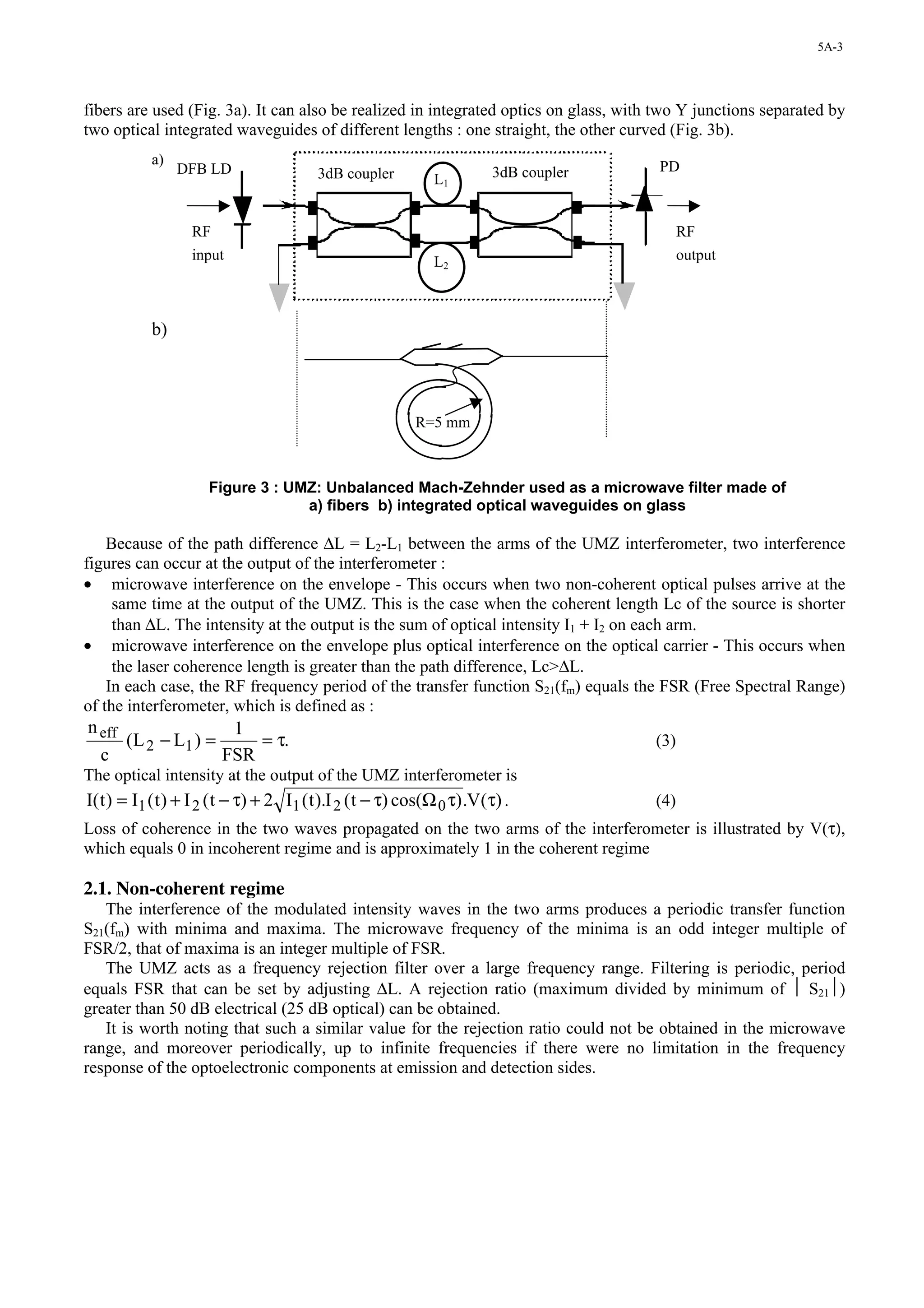
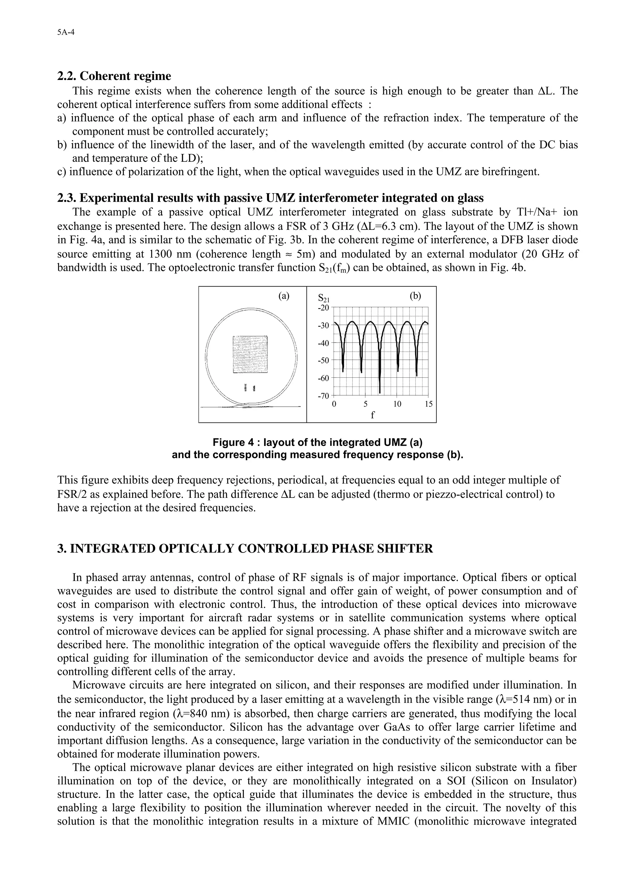
![5A-5
circuits) and OEIC (optoelectronic integrated circuits). The silicon technology chosen offers a large maturity
and allows a high integration level while the SOI technology (used here for monolithic integration) is very
promising for microwave applications, because of the low propagation loss. The optically passive controlled
devices can be further co-integrated with MMIC on silicon, to realize sub-systems like optically controlled
VCO, amplifiers...
3.1. Optical controlled microwave switch on bulk silicon
Here a high resistive (5000 Ω.cm) is used and aluminum coplanar lines are etched on top of it.
The gap (see Fig. 6) inserted in the signal line acts as a microwave phase shifter and as a switch, both
controlled by the light emitted by a laser diode (λ = 840 nm). Note that here, only a bulk silicon substrate is
used and illumination is made on top of the cell. The gap size is of the order of 16µmX100 µm. After on-wafer
calibration, S parameters have been measured for both dark (“off”) and illuminated (“on”) states.
The variations of S21 with frequency are shown in Fig. 5 in the "off" and "on" state.
Figure 5 : S21(f) for the microwave switch on bulk silicon
A large on/off ratio can be obtained; the value is 20 dB around 6 GHz with 15mW of optical power,
and the insertion loss is around 8 dB.
3.2. Optically controlled switch integrated on a SOI type structure
Here, we discuss optical integration of the illuminating waveguide.
Guided wave optics based on Silicon-On-Insulator have gained interest since they offer low cost and well
established technology [3] and they are compatible with monolithic microwave integrated circuits in CMOS
and BiCMOS technology that works now in the GHz range. The etched buried channel optical waveguide used
here and realized in this technology has been fabricated at CEA/LETI in Grenoble [4] and the fabrication
procedure has been given in details in Ref. [5-6]. In the final integrated structure of Fig. 6, the polysilicon gap
inserted in the signal strip of a coplanar waveguide is optically controlled by the monolithically integrated
optical waveguide embedded in the SOI structure. Here, two illuminating conditions are compared : top fiber
illumination with optical power of 2.4 mW and integrated illumination with optical power of 2 mW. It can be
concluded from Fig. 7 that the same switching performances can be observed whatever the way of illumination
is.](https://image.slidesharecdn.com/en-028-all-120926115440-phpapp01/75/En-028-all-83-2048.jpg)
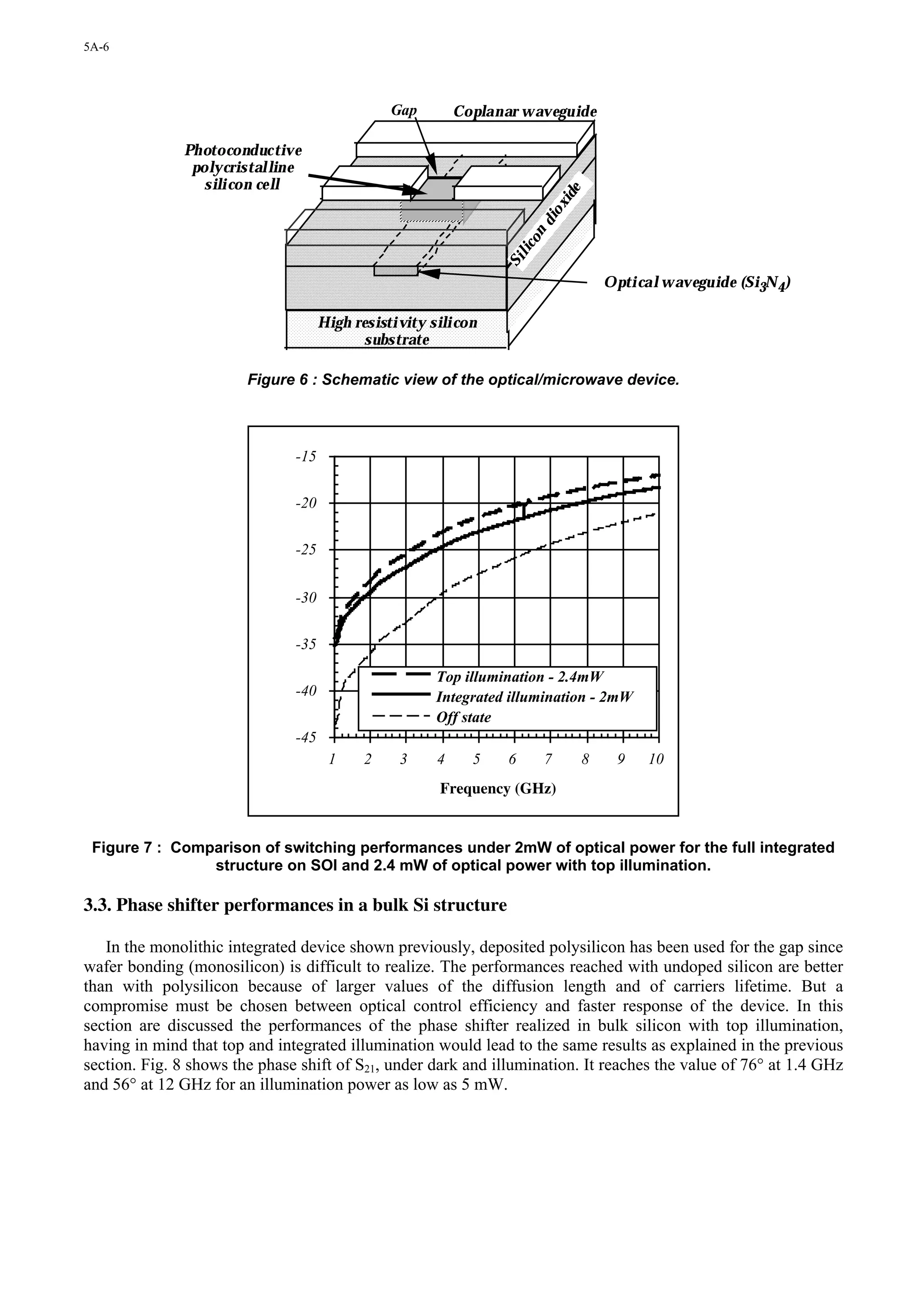
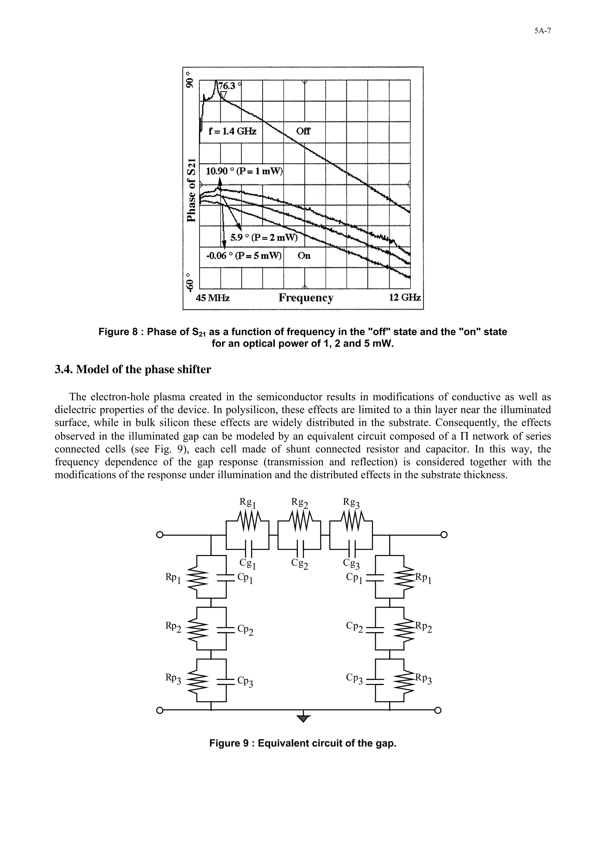
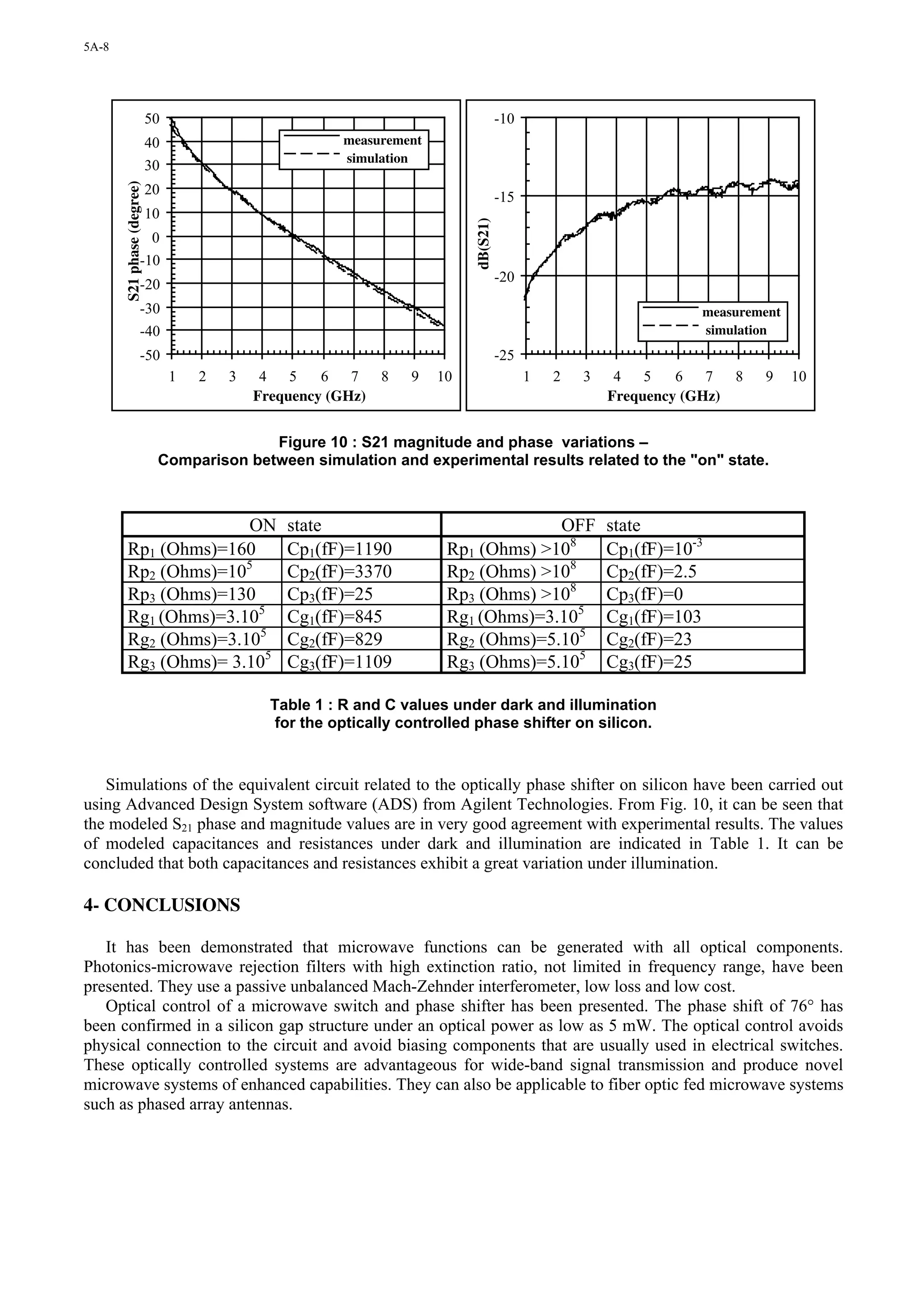
![5A-9
References
[1] An Ho Quoc, “Etude et Réalisation de Dispositifs Tout-Optiques pour le Traitement de Signaux Rapide”,
PhD thesis, INPG Grenoble, France, July 1996.
[2] T.A. Cusik, S. Iezekiel, R.E. Miles, S. Sales, J. Capmany, “Synthesis of All Optical Microwave Filters
Using Mach Zehnder Lattices”, IEEE Trans. on Microwave Theory Tech., vol. MTT-45, pp. 1458-1461,
August 1997.
[3] U. Hilleringmann and K. Goser, “Optoelectronic System Integration on Silicon, Photodetectors and VLSI
CMOS Circuits on One Chip”, IEEE Trans. Electron Devices, vol. 42, pp. 841-845, 1995.
[4] P. Mottier, “Integrated Optics at LETI”, International Journal of Optoelectronics, Vol. 9, Nr 2, pp. 125-
134, 1994.
[5] S. Chouteau, B. Cabon and J. Boussey “Integrated Optics on Silicon substrate for Microwave
Applications”, 28 th European Microwave Conference, Amsterdam 6-8 October 1998, Proc. pp. 70-74.
[6] S. Chouteau, J. Boussey, B. Cabon, A. Illiadis, “Optoelectronic Microswitch on SOI Based Structure”,
IEEE International SOI Conference, 1995, Proc. pp. 40-41.](https://image.slidesharecdn.com/en-028-all-120926115440-phpapp01/75/En-028-all-87-2048.jpg)

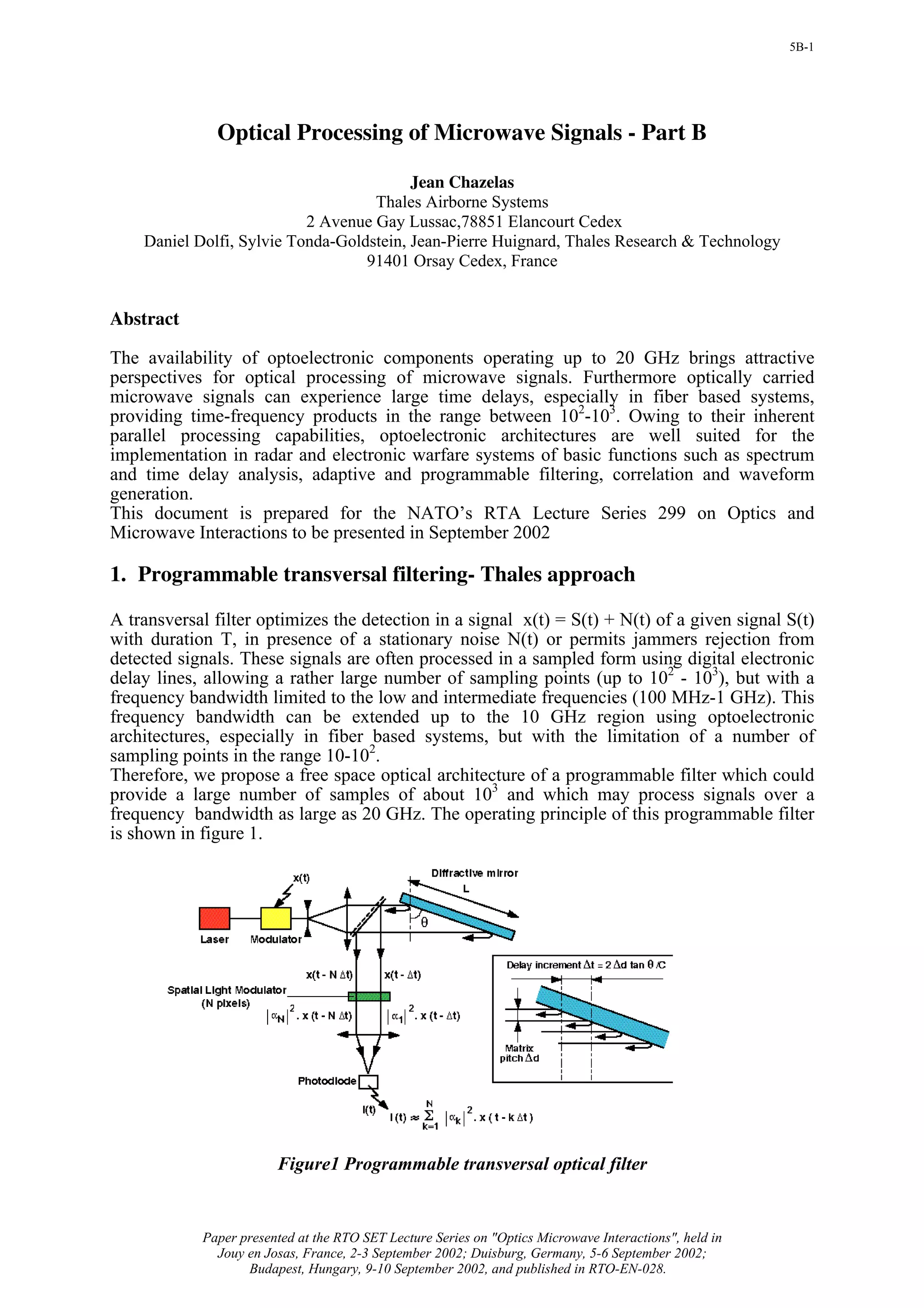
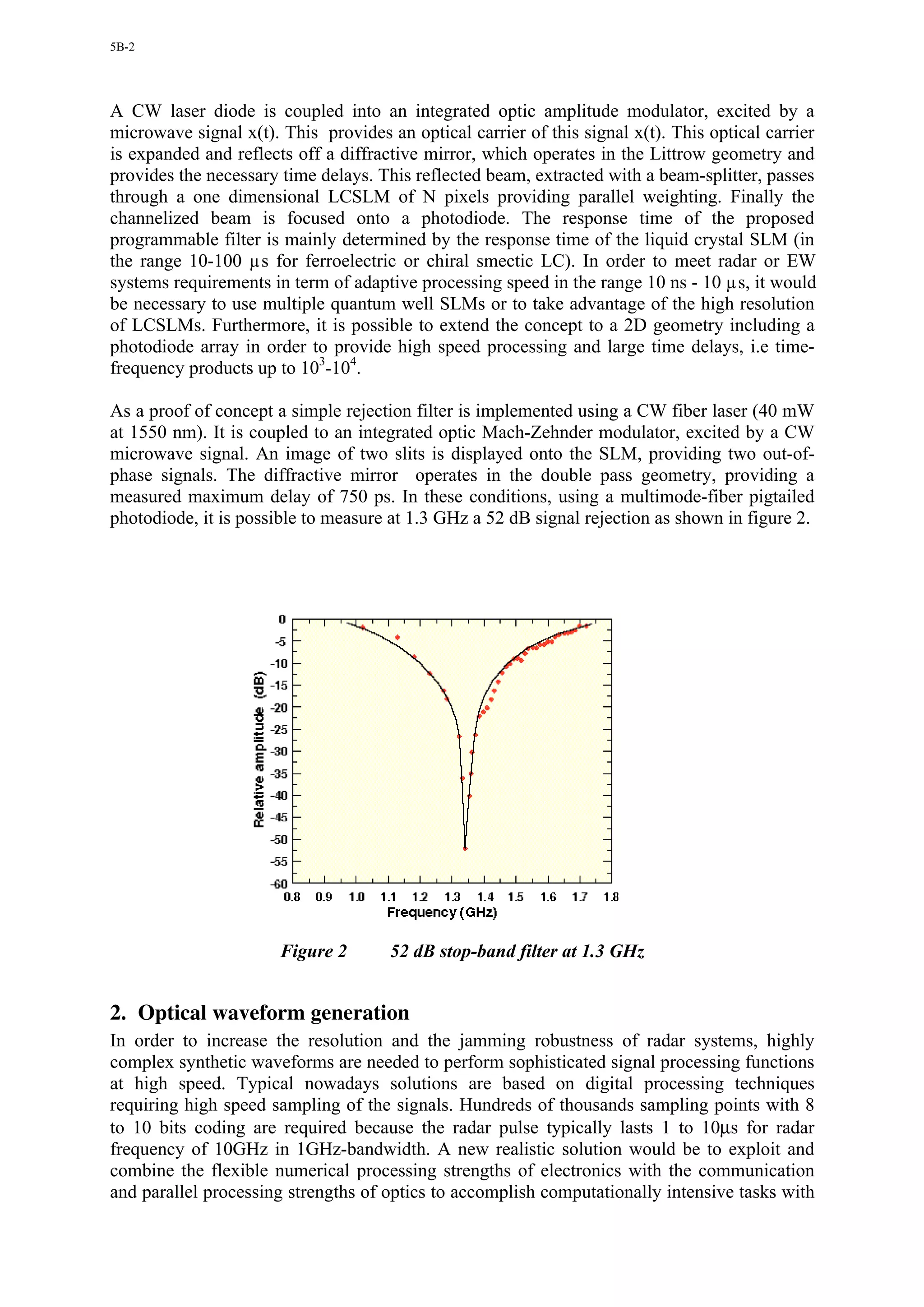
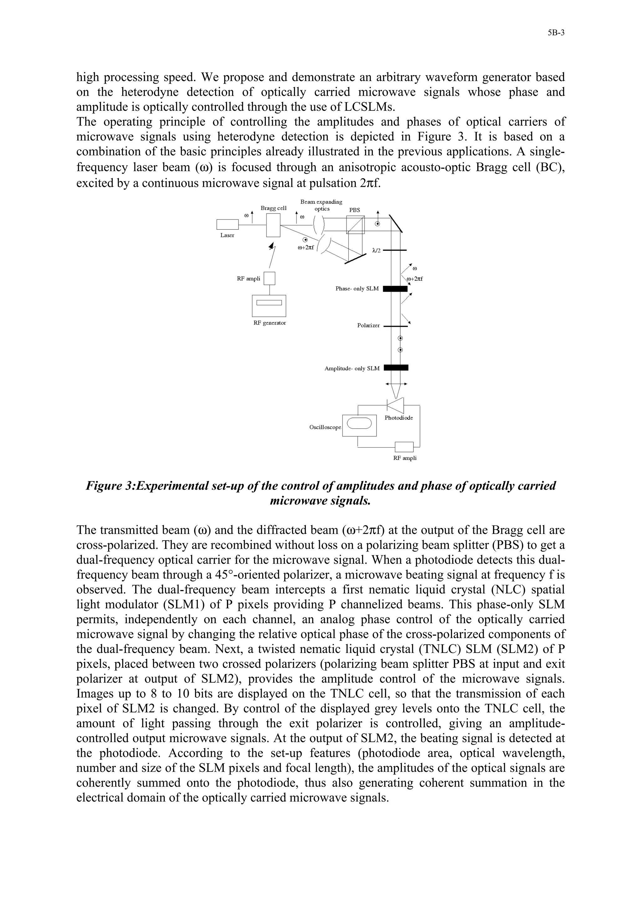
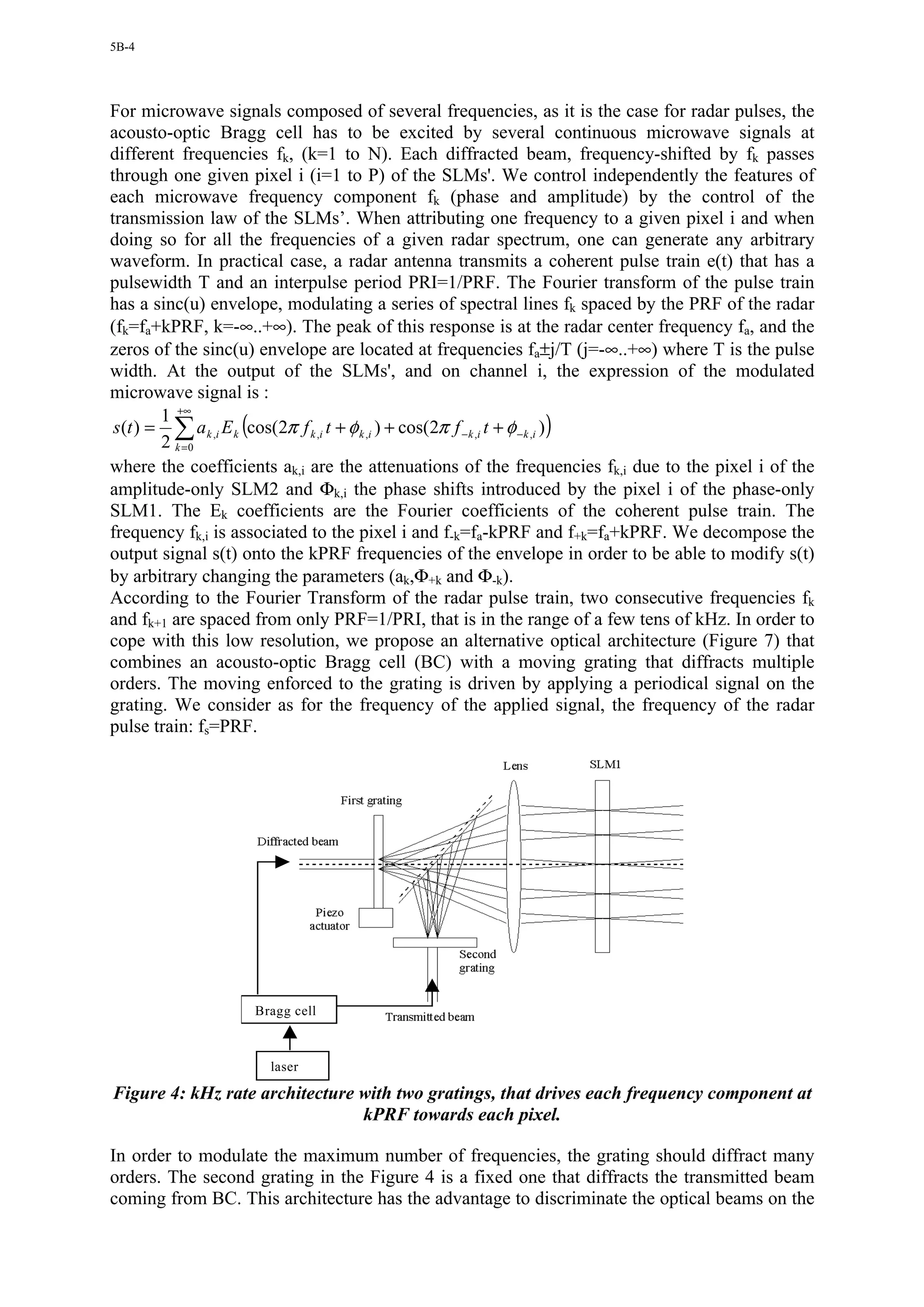
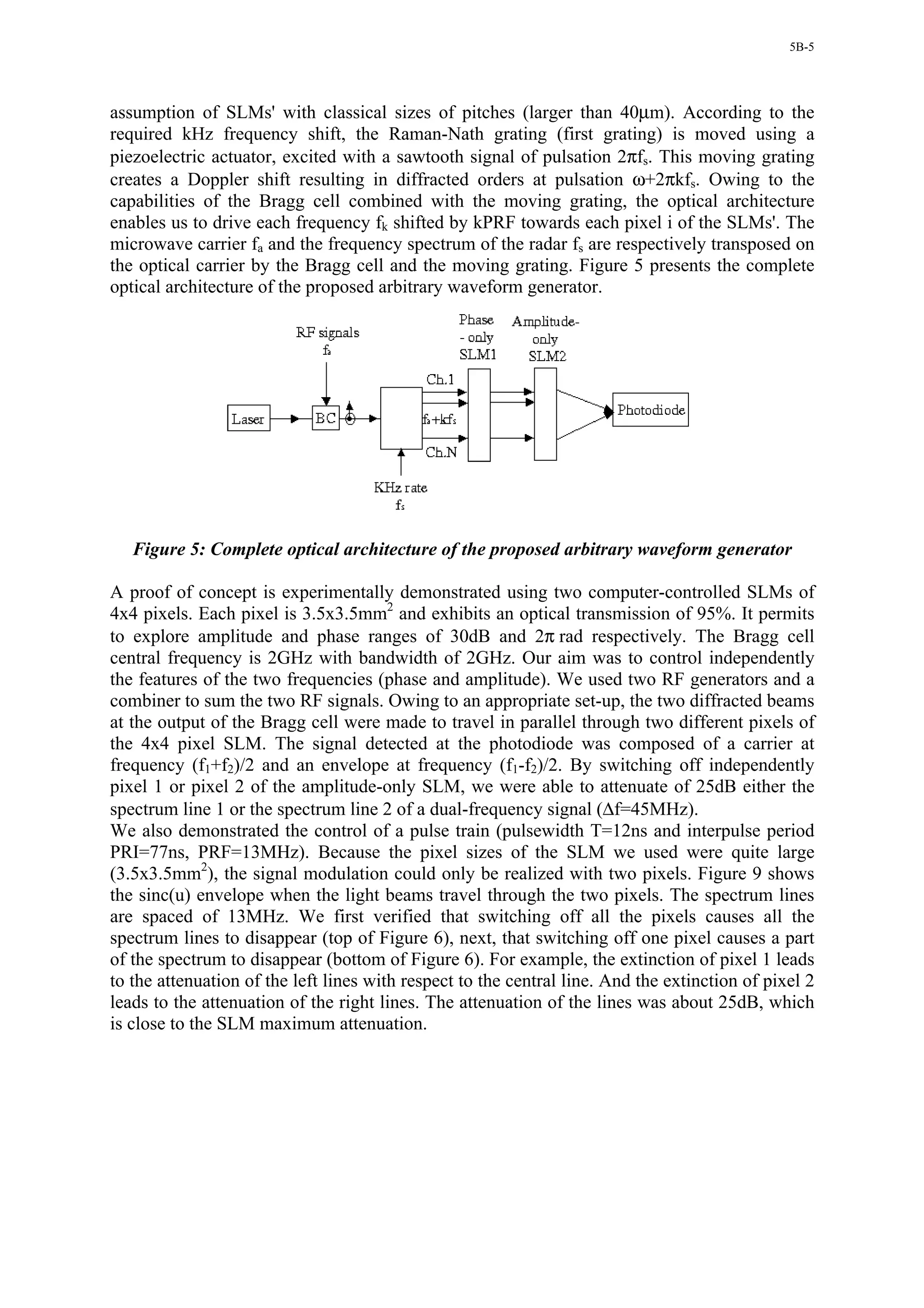
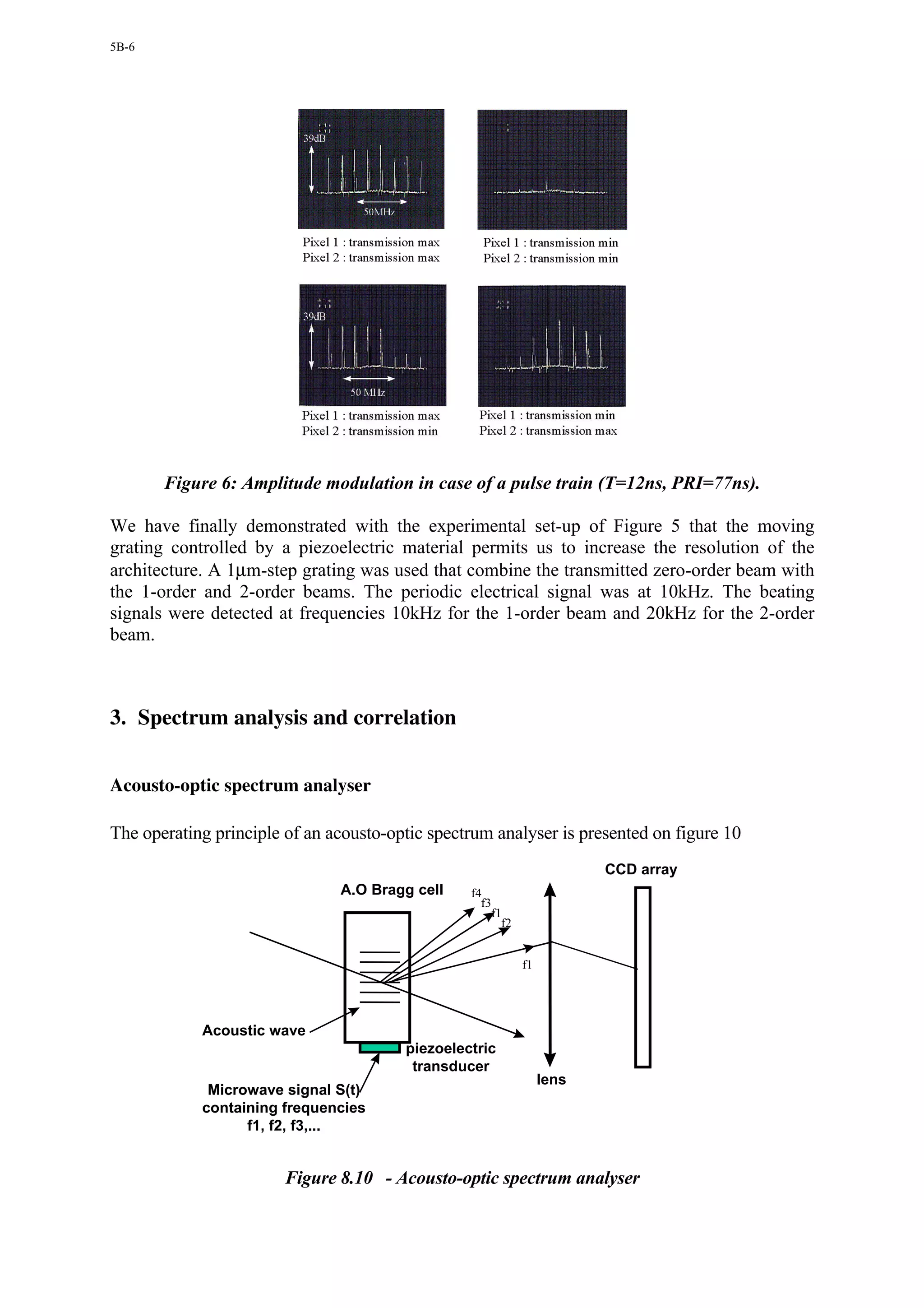
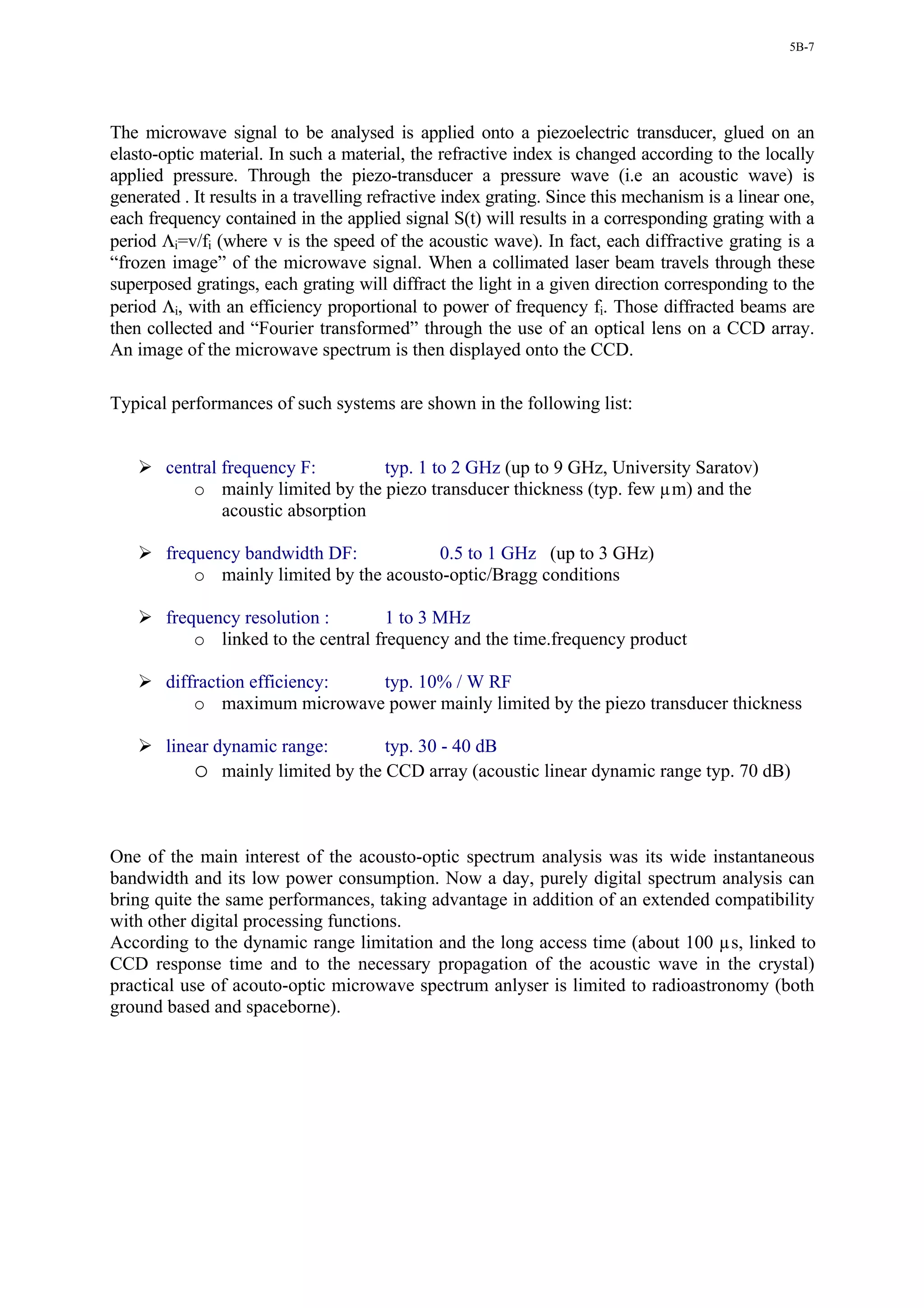
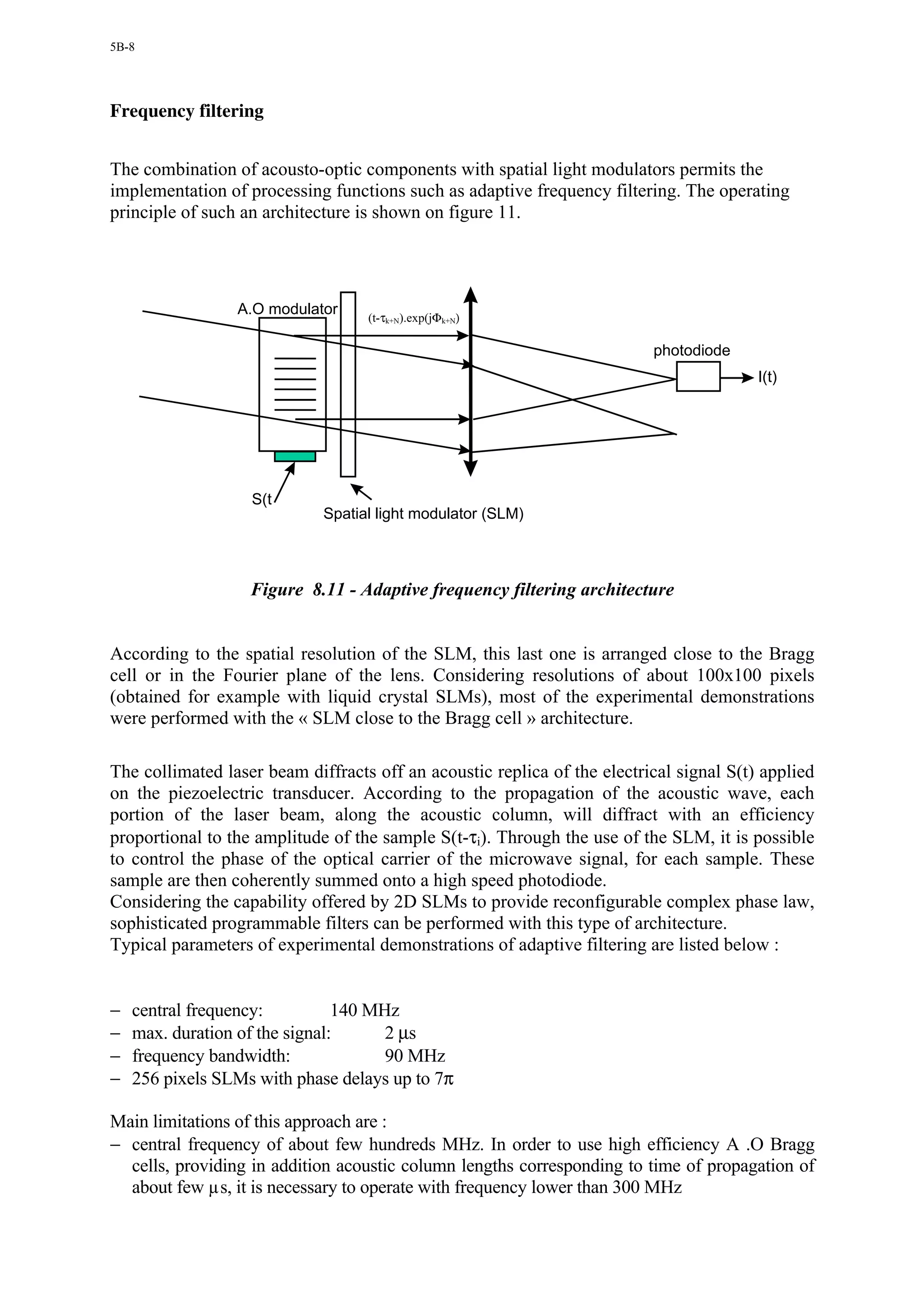
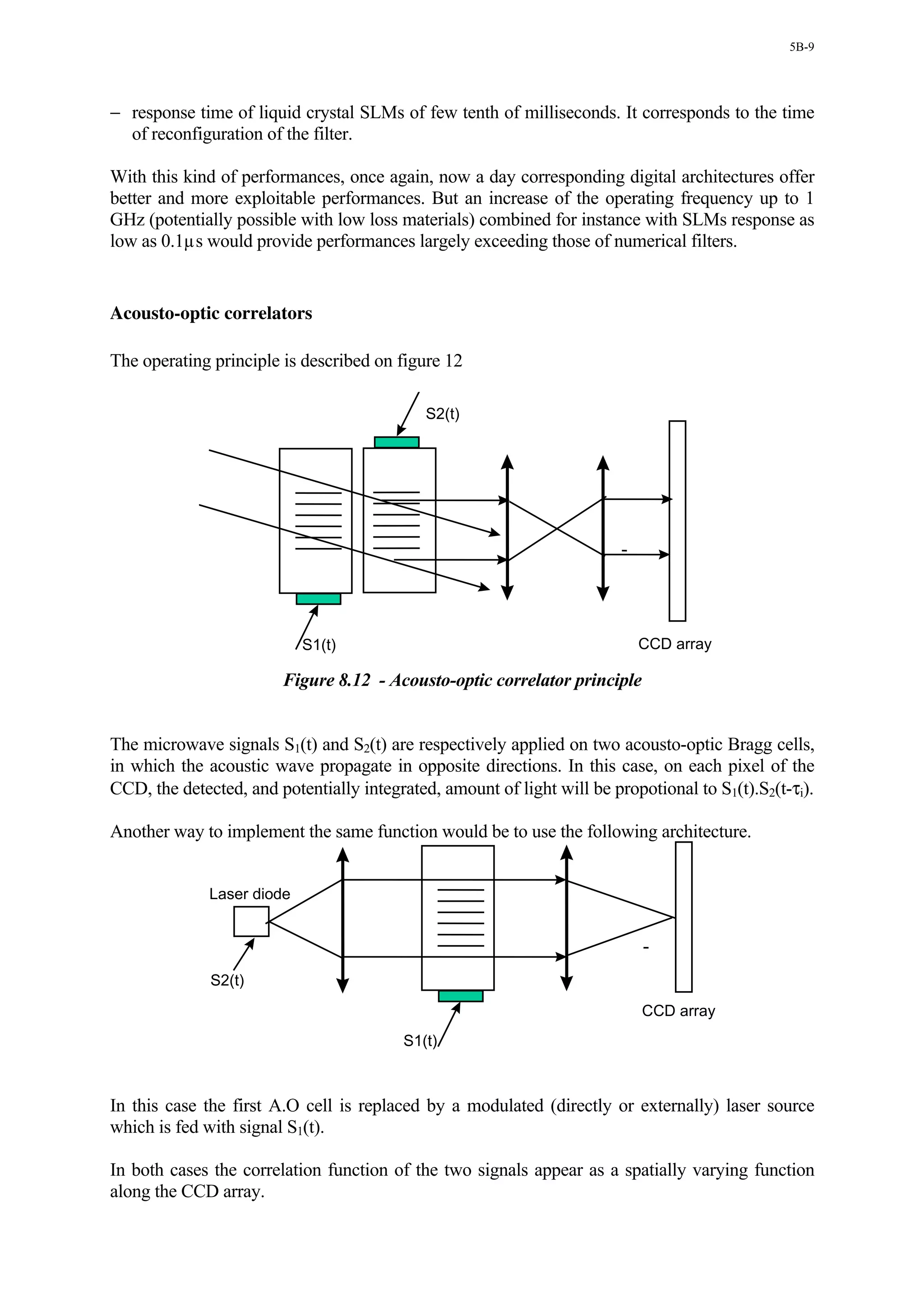
![6-1
Opto-Microwave Signal Processing:
Up and Down Conversion Techniques
Tibor Berceli
Márk Csörnyei
Budapest University of Technology & Economics
1111 Budapest
Goldmann György tér 3, Hungary
1. Introduction
This application note introduces the concepts of opto-microwave signal processing used in several
communication systems today. Emphasis is placed on optical-microwave up- and down conversion
techniques.
In today’s and future mobile- or local area networks (LAN) there is a need for optically supported network
technologies with a few sophisticated central stations serving a big number of quite simple and cheap optical
terminals, such as small base-stations in millimeter-wave optical-wireless local multipoint distribution systems
(LMDS), computer or CATV networks. The right answer for all of these challenges is the subcarrier
modulated optical transmission.
The subcarrier optical data transmission method offers several advantages over the generally applied TDMA
(time division multiple access) system. In a TDMA system the transmitters of the stations are operated on a
time sharing basis. In the receivers direct optical detection is used. In a high bit rate data communications
network a digital signal processing system with complete capacity should be applied both in the transmitters
and in the receivers. That is a big disadvantage which limits the future enhancement of the network capacity.
In case of the subcarrier type optical data communications the transmission capacity of the network can be
increased by applying new subcarriers, and thus the digital signal processing system can be kept with
unchanged bit rate. The transmitters are used in a continuous operation and in the receivers a heterodyne type
detection can be applied which provides a lower noise figure. The continuous operation of the transmitters
makes possible several connections working at the same time.
The present method used for reception is rather complex and therefore somewhat troublesome because it
applies a tuned filter. Utilizing an opto-microwave mixer there is no need for a tuned filter and thus it is
suitable for monolithic integration.
1.1. SUBCARRIER TYPE DATA COMMUNICATIONS
The principle of the subcarrier type data communications is presented first. Each transmitter has its own
subcarrier frequency (or frequencies); however, the receivers are tuned to make connection with any
transmitter. Thus there is no need for switching in the network because the requested connection is established
by tuning the receiver to the wanted subcarrier frequency.
To establish a connection between the stations a signaling channel and a central control unit are applied [1],
[4]. An individual subcarrier serves for that purpose applying on/off modulation with a low bit rate and time
sharing for the transmitters and receivers. A control unit has a photodetector for the reception of the calling
signals coming from the transmitters. The control unit emits ringing signals and control signals for the
receivers. The control signal contains the information which subcarrier frequency has to be received by the
specific receiver.
The block diagram of the transmitter is shown in Fig. 1. The information signal is modulating the subcarrier
frequency. The signaling information is transmitted in a similar way. The subcarrier frequency of the signaling
channel is the same for all of the transmitters and receivers. That common signaling channel is used on a time
sharing basis. However, the subcarrier frequencies of the information channels are different.
Paper presented at the RTO SET Lecture Series on "Optics Microwave Interactions", held in
Jouy en Josas, France, 2-3 September 2002; Duisburg, Germany, 5-6 September 2002;
Budapest, Hungary, 9-10 September 2002, and published in RTO-EN-028.](https://image.slidesharecdn.com/en-028-all-120926115440-phpapp01/75/En-028-all-101-2048.jpg)
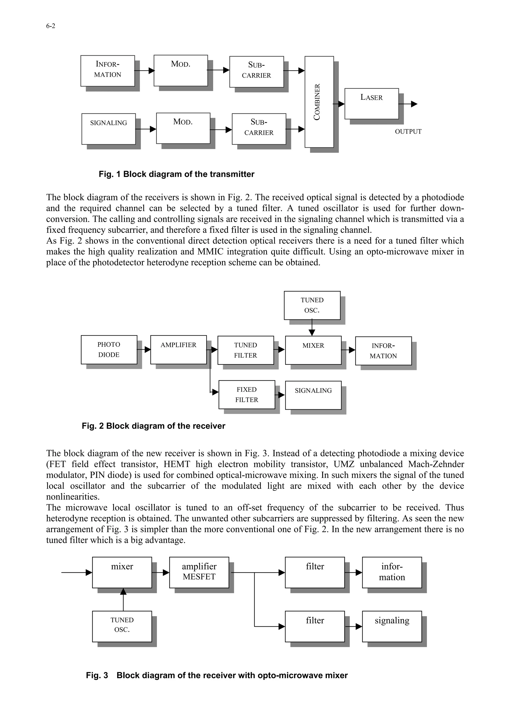
![6-3
2. Opto-microwave mixing by MESFETs
This chapter presented here concerns the mixing of a microwave signal with a modulated optical signal in a
MESFET. A brief theoretical analysis of the mixing mechanism is given in terms of the input signal
parameters and device characteristics. Experimental results for the IF response of the MESFET as a function
of RF frequency, incident optical power, optical modulation depth and gate bias voltage are shown.
The basic motivation for the research presented here is the chip-level integration of microwave and photonic
components. It is demonstrated that a microwave signal can be mixed with a modulated optical signal in a
MESFET, the most commonly used device in MMIC’s, for the up- and down-conversion of microwave
signals.
2.1. PHOTORESPONSE OF THE MESFET
The following discussion is based on recent work by Malone and Paolella at.al. [1] and [3] related to the
internal photovoltaic effect in the MESFET, which gives rise to photoresponse in the device. In the internal
photovoltaic effect, illustrated in Fig. 4, the absorbed photons modulate the channel-substrate barrier, thereby
modulating the channel height. In effect, the light acts as an “optical gate.” We take advantage of this effect to
mix an optical signal with a microwave signal in the device.
Fig. 4 Internal photovoltaic effect in a GaAs MESFET. The difference in doping level between the epi
and substrate layers produces a potential barrier in the standard MESFET, as shown in (a). When
illuminated the potential barrier is reduced, as depicted in (b), thereby increasing the channel height
(optical gate).](https://image.slidesharecdn.com/en-028-all-120926115440-phpapp01/75/En-028-all-103-2048.jpg)
![6-4
The drain-source current photoresponse for a MESFET was measured as a function of gate-source voltage.
The optical signal can be derived from medium power laser operating at 850nm. An optical attenuator controls
the power to the MESFET. The optical signal is routed to the MESFET via a cleaved output fiber positioned
over the MESFET.
The measured results are presented in Fig. 5. The drain current photoresponse is determined by the
measurement of the drain current in the dark and the drain current under illumination, and is expressed as
I ph = I d (illuminated ) − I d (dark) (1)
Fig. 5 Drain current photoresponse of the MESFET as a function of gate-source voltage
The photoresponse of the drain current is due to the internal photovoltaic effect and is given as
I ph = g mV ph (2)
where gm is the transconductance of the device. Vph is the optically induced photovoltage[1],[14], which can
be written approximately as
V ph ≈ c1 (L0 )P + c1 p(L0 ) (L − L0 ) + ...
( p −1)
(3)
where L is the optical intensity, and L0 is the optical intensity at the operation point. The higher power terms
are omitted. The coefficients c1 and p depend on the specific MESFET. To obtain the coefficients, the
photovoltage was measured as a function of optical intensity. The measured relationship was approximated
using a curve fitting method.
In Fig. 5 the maximum optical intensity of 3.5mW is used as the 0dB reference, and for each successive curve
the intensity is attenuated by 3dB. Under small signal conditions the photoresponse follows the
transconductance (gm) of the device, which is essentially constant with gate bias from 0 to -0.5V. The
photoresponse is dominated by the product of the internal photovoltage and gm when no external resistance is
connected to the gate (i.e., Rg=0). As optical intensity is increased, there are contributions to the
photoresponse from the substrate photocurrent and the photoconductive current in the channel. The internal
photovoltage which is an exponential function will be large resulting in a significant photoresponse well
beyond the pinch-off.
2.2. MIXING MECHANISM IN THE MESFET
The mixing effect is the result of the device nonlinearities. In general all elements of the internal equivalent
circuit exhibit some nonlinearity, however the dominating factor is the nonlinearity of the drain-source current
versus gate-source voltage characteristics. A small effect is obtained from the nonlinear gate-source
capacitance as well.](https://image.slidesharecdn.com/en-028-all-120926115440-phpapp01/75/En-028-all-104-2048.jpg)
![6-5
The drain-source current is expressed as a power series of the gate-source voltage at a constant drain-source
voltage
( ) 2
( )
I d = I db + a1V gl + a 2 V gl + a3 V gl + ...
3
(4)
where a1,a2 and a3 are coefficients that depend on the drain-source voltage and Idb is the dc quiescent point. Vgl
is the gate-source voltage under illumination.
The effect of illumination on the drain-source current is taken into account by introducing the optically
induced photovoltage Vph which is dependent in the light intensity. Thus in case of illumination the gate-
source voltage is the sum of the electrically applied voltage and the photovoltage
V gl = V g + V ph . (5)
The lightwave illuminating the device is modulated:
L = L0 [1 + m cos(ω1t )] (6)
where L0 is the average optical intensity, and ω1 and m are the modulation frequency and depth, respectively.
A microwave signal is simultaneously applied across the gate and source
V g = Vs 0 cos(ω 2 t ) + V gb (7)
where Vs0 is the amplitude, ω2 is the angular frequency of the microwave signal, t is the time, and Vgb is the
biasing gate-source voltage.
Thus the gate-source voltage under optical illumination is the sum of the electrically and optically induced
voltages
V gl = V gb + V ph 0 cos(ω1t ) + Vs 0 cos(ω 2 t ) (8)
where Vph0 is the amplitude of the photovoltage
V ph 0 = c1 pm(L0 )P. (9)
The mixing product in the drain-source current at the intermediate frequency ω2-ω1 is obtained by substituting
(5) into (4)
I dmix = a 2V ph 0Vs 0 . (10)
For this result we assume that the second order nonlinear term of (4) is much larger than the higher order
terms (i.e. small-signal case). This simplified theoretical derivation shows the dependence of the mixing
product in the drain-source current on all the parameters of the microwave input Vs0, optical input L0, and m,
as well as the device characteristics, a2, c1, and p.
The other nonlinearities of the device can also influence the mixing product; however, their contribution is
small. Nevertheless, some effect is obtained from the nonlinearity of the gate-source capacitance. The two
signals, i.e. the electrically and the optically induced signals are mixed in the nonlinear gate-source
capacitance and then they are amplified due to the transconductance of the device. The capacitive mixing
product in the drain-source current is expressed as
I dnux / cap = αccVs 0V ph 0 / 2 (11)
where α is a coefficient presenting the part of the optically induced voltage Vph which effects the gate-source
capacitance, and cc=∂Cgs/∂Vg being the derivative of the gate-source capacitance with respect to the gate-
source voltage. The parameter cc, represents the part of the photovoltage which influences the gate-to-source
capacitance. That influence was measured and a curve fitting method was used to obtain cc. The parameter α
was estimated based on the construction of the FET used. The mixing products in the drain-source current are
presented in Fig. 6 based on the measurements performed recently to determine the elements of the MESFET
under optical illumination [1]. In Fig. 6 the conversion ratio is plotted with and without capacitive mixing as a
function of the gate-source voltage. The conversion ratio is defined as
Cr = I dmix Vs 0V ph 0. (12)
As seen in Fig. 6 the contribution of the nonlinear gate-source capacitance is quite small. Some noticeable
effect is only observed around the minimum conversion ratio where the drain-source current nonlinearity
produces a small mixing product.](https://image.slidesharecdn.com/en-028-all-120926115440-phpapp01/75/En-028-all-105-2048.jpg)
![6-6
Fig. 6 Conversion ratio as a function of the gate-source voltage with and without capacitive mixing
2.3. COMPARISON OF “DIRECT” AND “INDIRECT” MIXING
There are two basic experimental setups concerning the MESFET as an O/E up- or down-converting front-end
in the optical receiver. In an “indirect” mixing configuration (Fig. 7), the MESFET serves as a detector for the
optical signal and the up- or down- conversion is performed in a conventional Schottky barrier mixer.
However, by taking advantage of the inherent nonlinearities of the MESFET, both detection and frequency
conversion of the modulated optical signal can be achieved in the device. This direct mixing approach, shown
in Fig.8, is in the focus of this note.
In both of the setups of Fig. 7 and 8 an 850nm wavelength laser can be used. This wavelength is defined by
the photosensitivity of the GaAs. The light is directly modulated by the RF Source 1 and positioned on the
gate fingers of the MESFET. In case of commonly used microwave transistors, the device should operate with
a reverse bias, for example with 0.5 volt at the gate and a drain-to-source voltage of 2 volts. As shown in eq. 9
and 10, the IF or the upconverted term of the drain current is dependent on the optical modulation depth m.
For the indirect mixing configuration, shown in Fig. 7, the MESFET was used as an optical detector. The
detected signal from the MESFET was mixed with the signal from RF Source 2 in an additional mixer. As a
baseline of comparison, indirect mixing can also be accomplished with a PIN photodetector in place of the
MESFET (the conventional optical detection followed by microwave mixing).
For the direct mixing configuration, in addition to the optical input, a signal from RF Source 2 was applied to
the gate of the device and the IF output was measured at the drain using a spectrum analyzer with an
appropriate resolution.
2.4. EXPERIMENTAL MIXING RESULTS
As an example there are some experimental mixing results for direct mixing with MESFET as an opto-
microwave mixer and for indirect mixing accomplished with p-i-n photodetector and a Schottky barrier mixer.
The MESFET in the example [1] is an ITT GTC213-1 with four 75µm wide gate fingers, a gate length of
0.8µm and a dopant concentration of 3x1017 cm-3. The device was operated with a reverse bias. For the direct
mixing approach, the signal from an 850nm wavelength laser with an 8GHz bandwidth was directly
modulated by an RF source and conveyed to the MESFET by an optical fiber. To maximize the IF response,
100% modulation depth was used on the laser, which has an average optical output power of 1.8mW.](https://image.slidesharecdn.com/en-028-all-120926115440-phpapp01/75/En-028-all-106-2048.jpg)
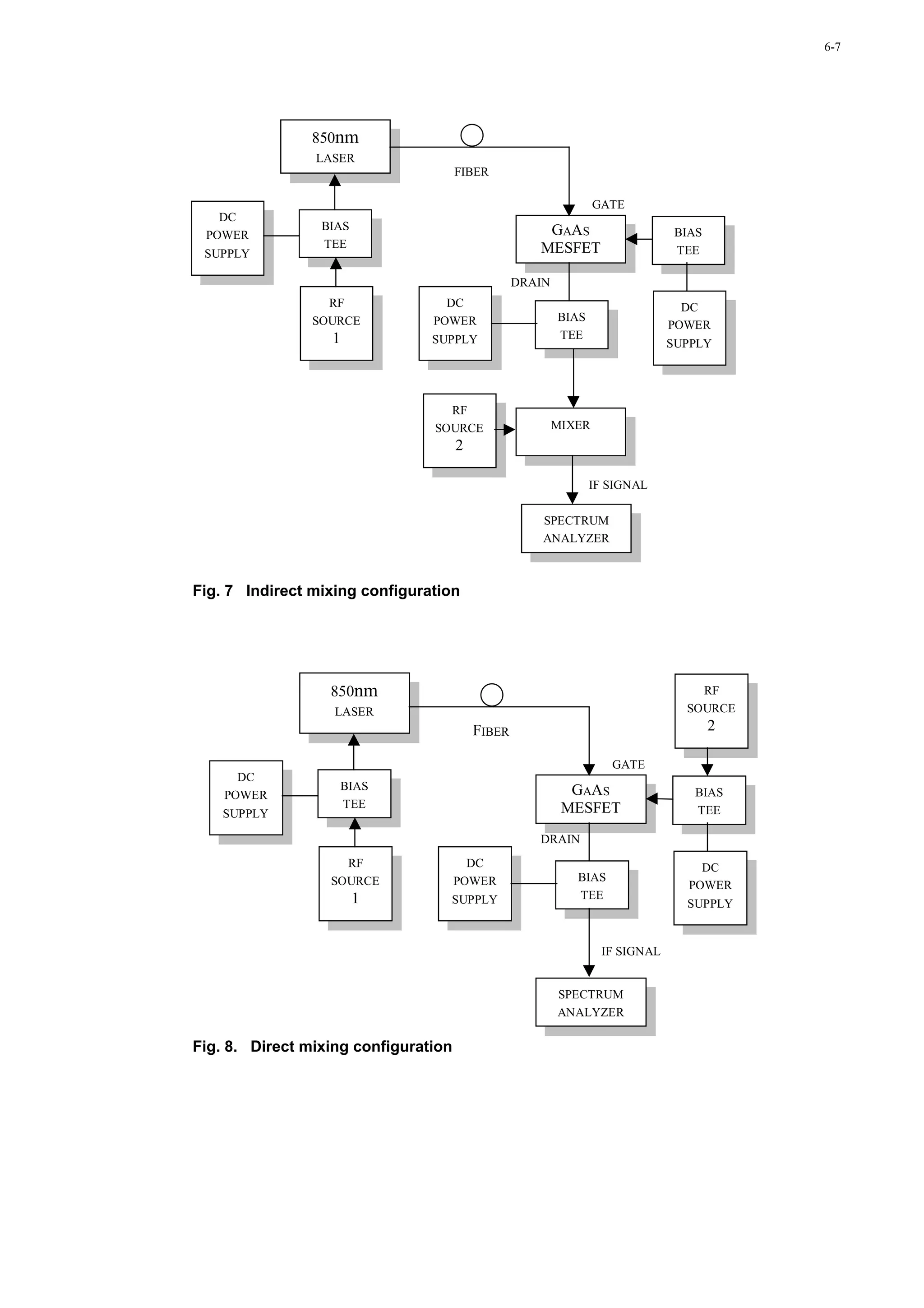
![6-8
The results of optical mixing with MESFET and the conventional detection and mixing with a p-i-n diode and
an additional mixer are depicted in Fig. 9. The p-i-n photodetector had a 10GHz bandwidth, a responsivity of
35mA/mW and a diameter of 25µm. The p-i-n operates in this example with a reverse bias of 8V.
IF response with MESFET
IF response with PIN/Schottky Mixer
IF is 50MHz
Fig. 9 IF response of the two mixing configurations
In that results of [1] IF response of the MESFET exceeds that of p-i-n/Schottky mixer combination up to an
RF frequency of about 700MHz. The IF response emulates the photoresponse spectrum of the device with a
conversion loss in range of 7-11dB. Under the same conditions the Schottky mixer had a conversion loss in
the range of 4-10dB (See Fig.10). Clearly, as these results show, the MESFET can be used as mixer with
optical and microwave inputs. Depending upon the particular application, the data may be an optical signal
and the local oscillator an electrical signal, or vice versa.
The dependence of the IF response of the device on the average incident optical power and the RF drive
power to the laser is shown in Fig. 11. The slope of the lines indicates that a 1dB decrease in optical power
incident on the device translates into a 2dB decrease in the IF response, as expected with square law behavior.
The figure also indicates that the IF response decreases linearly with RF drive power to the laser (modulation
depth). The conversion response of the MESFET is also strongly dependent on the gate bias voltage. A plot of
the IF response versus source-gate voltage at various RF frequencies is shown in Fig. 12. The IF response is
maximized when the gate is reverse biased at around 0.5V, which is also the bias voltage at which the
transconductance of the device is maximized. Larger reverse bias voltage on the gate decreases the IF
response significantly due to a reduction in the gain. However, at bias voltages larger than 1.8V the IF
response increases again. This is most likely due to the voltage dependence of the nonlinear coefficient a2.
The system noise figure is presented in Fig. 13 as a function of the RF frequency. In the figure 3 curves are
plotted: one for the p-i-n/Schottky mixer configuration and two for the MESFET with different bias voltages.
The noise is significantly smaller with a bias voltage close to pinch-off because then the drain-source current
is also smaller. As seen the system noise figure below 1000MHz is smaller in the case of the MESFET than
with the p-i-n/Schottky mixer configuration if a bias voltage close to pinch-off is used. However, the system
noise figure above 1000MHz is higher in the case of the MESFET compared to the p-i-n/Schottky mixer
setup.
2.5. COMPARISON OF DYNAMIC PROPERTIES OF DETECTION AND MIXING, BY FET DEVICES
According to the detection measurements of Berceli et.al. [5] by FET devices, the detected signal exhibits a
decay with increasing modulation frequency. The decay is relatively slow at low modulation frequencies. The
measurement result is in accordance with the recently published theoretical and experimental investigations.](https://image.slidesharecdn.com/en-028-all-120926115440-phpapp01/75/En-028-all-108-2048.jpg)
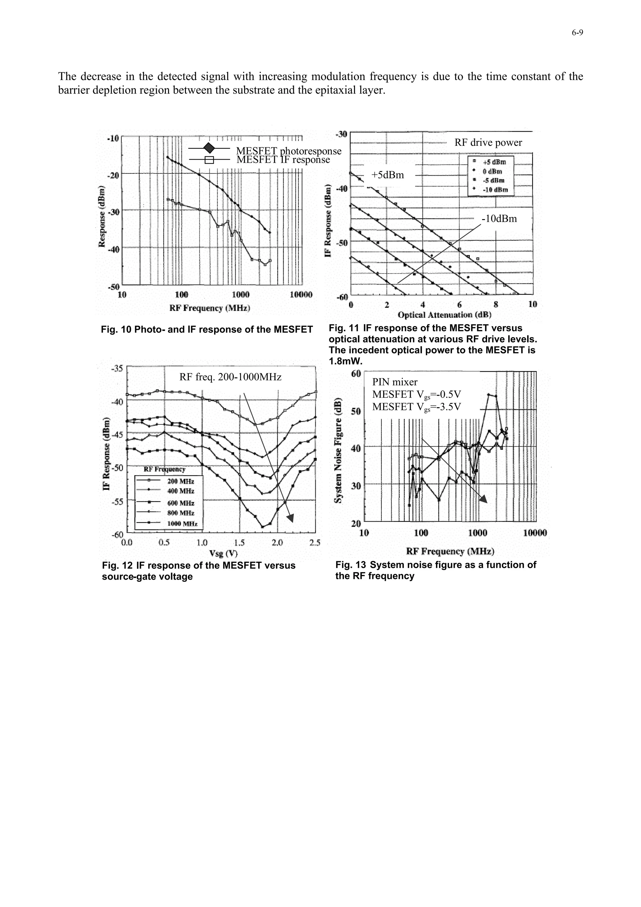
![6-10
The next question is whether the dynamic properties in the detection mode and in the conversion mode of
operation are the same.
In the tests investigating the dynamic properties of opto-microwave mixing by FET’s, both the optical and
microwave gates are driven by signals. Between the gate and source a microwave signal is applied while the
intensity modulated signal of a semiconductor laser diode is used to illuminate the active device. The
frequency dependence is different, the decay in the converted signal is much higher at low modulation
frequencies, and it is more pronounced with increasing modulation frequency compared to the frequency
response of the detected signal.
Another significant deviation is that the decrease in the converted signal is proportional to modulation
frequency, however, the decrease in the detected signal is developed slowly when the modulation frequency in
increasing. The reason of the differences in the dynamic characteristics is the following.
In the detection mode of operation the optically generated charge carriers are contributing to the detected
electric current in both depletion regions below the gate and between the substrate and the epitaxial layer by
changing the height of the conductive channel. Beside that effect the charge carriers generated in the substrate
are also participating in the detected current. Therefore, the frequency dependence of the detected signal is
determined by the conductive channel and the substrate currents.
On the other hand, in the mixing mode of operation the contribution of the substrate current in the generation
of the mixing product is negligible because in the substrate there is neither a nonlinear nor a parametric effect.
The mixing products are created mainly in the conductive channel. This way their power level is somewhat
lower and their frequency dependence is higher. There are two reasons for it: the time constant exhibited by
the depletion region between the substrate and the epitaxial layer and optically induced substrate current
which is increasing with the modulation frequency and doesn’t contribute to the mixing effect.
2.6. SINGLE SIDEBAND OPTICAL-MICROWAVE MIXERS
As mentioned in section 2.2 the mixing product in the drain-source current at the difference of the input
frequencies (ω2-ω1) is:
I dmix − = a2V ph 0Vx 0 (13)
The mixing product in the drain-source current at the sum of the input frequencies (ω1+ω2) is obtained as
follows [4]:
I dmix + = a2V ph 0Vs 0
*
(14)
Vs0 is the complex amplitude and Vs0* is the conjugate of the complex amplitude of the microwave signal
applied across the gate and source. Vph0 is the amplitude of the photovoltage.
Comparing these equations it can be seen that there is a phase difference between the mixing product current
amplitudes Idmix- and Idmix+ because of the conjugation of the microwave signal amplitude in the second case.
That makes possible to construct a single sideband optical-microwave mixer arrangement if two mixers are
applied in the two branches of a hybrid and 90° phase difference is established between the outputs of the
hybrid driving the mixers by the microwave signal. Due to the conjugation of the microwave signal the mixers
will provide 180° phase shift in the mixing product current amplitudes which makes possible their separation
by another hybrid. A switch is used for choosing the right mixing product for further signal processing.
The principle of the single sideband optical-microwave mixer is presented in Fig. 14, [4].
For the subcarrier type signal reception an important requirement is the high suppression of the image
frequency. This is achieved if the mixing products in the two branches are of equal amplitude with a 180°
phase difference. However, both the amplitude and the phase of the mixing product are frequency dependent.](https://image.slidesharecdn.com/en-028-all-120926115440-phpapp01/75/En-028-all-110-2048.jpg)
![6-11
MOD. LIGHT UPPER SIDEBAND
MIXER
IF HYBRID
SWITCH
TUNED LO RF HYBRID FILTER
IF SIGNAL
MIXER
LOWER SIDEBAND
Fig. 14 Block diagram of the new single sideband optical-microwave mixer
3. Optical-microwave double mixing by PIN diodes
The commonly used optical receivers apply mainly photo-diodes to detect the optical intensity modulated signal. A
relatively high sensitivity is achieved by properly matched transimpedance or distributed amplifiers.
In another method the modulated optical signal is mixed with a microwave signal in the photodiode producing an
intermediate frequency signal. Thus, heterodyne type reception is feasible. However the mixing conversion has a higher
loss compared to the direct detection.
In the double optical microwave mixing approach the conversion loss is much less than that of direct detection offering a
significant improvement in the reception sensitivity. The mixing product is even further increased by resonance
enhancement providing 20dB improvement in comparison to direct detection.
3.1. DOUBLE MIXING PRINCIPLE
This method of Berceli and Járó [7] utilizes simultaneously two effects: a direct and an indirect mixing of the modulated
optical signal and the microwave local oscillator signal. For direct mixing the bias is chosen close to the zero voltage
where the photo current is highly dependent on both the illumination intensity and applied voltage. Therefore the mixing
product is high. At the same time a detection of the optical signal is also obtained which produces a detected signal in the
base band. If this signal is reflected back to the photodiode it will also be mixed with the microwave local oscillator
signal. Thus the output signal is the resultant of two mixing procedures: an optical-microwave and an electrical mixing
(after optical detection).
The double mixing approach [7] is experimentally presented utilizing a 1A358 type CATV p-i-n photodiode. The setup
of optical-microwave circuit is shown in Fig. 15.
-6 -5 -4 -3 -2 -1 0 1
0
0.1 mW Vpd [V]
0.2 mW
-0.2
0.3 mW
0.4 mW
0.5 mW -0.4
0.6 mW
0.7 mW -0.6
0.8 mW
0.9 mW
Iphoto [mA]
1.0 mW -0.8
-1
Fig. 15 Optical-microwave mixing Fig.16 Measured DC characteristic of
setup the pin photodiode](https://image.slidesharecdn.com/en-028-all-120926115440-phpapp01/75/En-028-all-111-2048.jpg)
![6-12
The embedding circuit can be optimized for detection or mixing. The dc characteristics of the p-i-n
photodiode is shown in Fig. 16. Here the detected photocurrent is plotted as a function of the bias voltage for
different illumination intensities. As seen close to the zero voltage bias point the curvature of the
characteristics exhibits a maximum. At this bias voltage the dependence of the photo-current on the light
intensity is also maximal. This coincidence ensures the high mixing product in the double mixing
approach.The p-i-n photodiode is embedded into a microwave circuit where the detected base band signal is
reflected. The photo diode is driven by a microwave local oscillator signal and at the same time it is
illuminated by an intensity modulated optical signal. The result is presented in Fig. 17.
Here the mixing product is depicted as a function of the bias voltage. The frequency of the applied local
oscillator was 3GHz and the modulation frequency of the intensity modulated optical signal was 540MHz. As
seen, about 10dB mixing gain can be achieved biasing the photodiode close to zero voltage.
Fig.17 Measured power level of the Fig. 18 Measuremtn setup for resonant
upconverted signal versus the reverse mixing using a “transmission setup”
bias voltage (parameter is the LO power)
3.2. RESONANT ENHANCEMENT
For further improvement the resonant enhancement method can be utilized. The base band and the microwave
band are separated by a branching filter as shown in Fig. 18. The reflection in the base band can be adjusted
using a sliding short circuit (varying inductance). This way the mixing product is enhanced in a narrow band.
The spectrum of the upconverted signal is plotted in Fig. 19.
In the investigations by [7], the frequency of the local oscillator is 2GHz, the photodiode is biased at –0.2V
and the series capacitor is 4.7pF. With these settings there is a resonant peak around 50MHz as shown in the
figure.
4dBm
Resonant peak
1dBm
-2dBm 0.2
Frequency, MHz
Frequency, MHz
Fig. 19 Measured power level of the Fig. 20 Measured power level of the
upconverted signal (parameter is the LO detected sigal in resonant condition
power) (transmission setup) (parameter is the reverse bias voltage)](https://image.slidesharecdn.com/en-028-all-120926115440-phpapp01/75/En-028-all-112-2048.jpg)
![6-13
The resonance can be measured at base band too. The measured detected spectrum at base band is shown in
Fig. 20 at different bias voltages. The peak of the detected spectrum is only an attenuated signal after the
series capacitor of the resonator. For comparison Fig. 21 shows the upconverted spectrum using the same
configuration setup without resonator subcircuit. In this case the embedding circuit was optimized for
detection. Comparing the curves of the Fig. 19 and 21 the effect of the resonance can be seen.
4dBm
1dBm
-2dBm
Fig. 21 Measured power level of the upconverted signal without resonator (parameter is the LO
power)
4. Frequency conversion methodes by optical interferometer and photodiode
According to [10], there is a comparison of the performance of two different optoelectronic configuration,
both used for frequency conversion in the microwave frequency range. In the firs case, mixing is achieved by
a Mach-Zehnder (MZ) interferometer, while in the second case, photodiode mixing is presented.
4.1. MIXING WITH UMZ/PD
In the firs case, the optical system used for microwave mixing is a distributed feedback (DFB) laser diode
(LD) directly modulated by two microwave frequencies, f1 (fLO corresponding to the LO signal) and f2 (in this
case, fRF) followed by an unbalanced MZ (UMZ) and a photodetector (PD). The system is shown in the upper
portion of Fig. 22.
The basic principle is the nonlinear (sinusoidal) intensity response of the UMZ interferometer/PD combination
as a function of the frequency of the optical field. Direct modulation generates FM, which is then converted to
AM using the UMZ interferometer working in the coherent regime. The PD detects the optical intensity which
is a quadratic function of the optical field, so frequency mixing is obtained. The originality of this solution is
the use of a passive optical device inserted in the optical link which generates mixing with better conversion
than classical solutions using active MZ modulators.
Fig. 22 Optical systems used for optical-
microwave mixing](https://image.slidesharecdn.com/en-028-all-120926115440-phpapp01/75/En-028-all-113-2048.jpg)

![6-15
Pdet Pmix [dBm]
VPD [V]
Fig. 23 Voltage dependence of the detected power and of the upper-sideband mixing product.
4.3. EXPERIMENTAL RESULTS WITH UMZ/PD
Measurements were made in [10] with a DFB LD emitting at λ=1300nm, having an Ith=13mA and a maximal
oscillation frequency of 2.5GHz. The dc-bias current was 22mA and the optical power coupled in the
interferometer was 420µW.
To operate in the coherent regime as wanted, the UMZ was realized using only two connectorized –3dB fiber
directional couplers. In this case, ∆L=1.6cm, which corresponds to FSR=13GHz.
The LO frequency was FLO=1.9GHz, with a power of –4dBm. The other modulation frequency, fRF was swept
from 2 to 2.5GHz and had a power of –18dBm. Fig. 24 shows the power spectrum of the intensity detected by
the PD and measured by a spectrum analyzer. In Fig. 24, the lower sideband of the mixing product, fLO-fRF, as
well as the third order intermodulation product, was significantly increased by inserting the UMZ. However,
the input frequencies fLO and fRF are not rejected. In fact, to obtain an optimal rejection of the fundamentals,
condition 1 should first be fulfilled, which was not the case under the conditions of operation. The relative
optical phase shift between the two arms is very sensitive to ambient variations, and during the experiments
the operating regime continuously varies between minimum and maximum transmission including the
quadrature. Secondly, the closer f1 would be to FSR/2=6.5GHz, the larger the rejection would be, and here
f1=fLO=1.9GHz (limitation due to the LD)
PLO, Pmix [dBm]
Pmix, Pdet [dBm]
at the input
at the output of
UMZ
Frequency [GHz] PLO injected at fLO=3GHz [dBm]
Fig. 24 Power spectra of detected signals Fig.25 Levels of first and second harmonic
with and without UMZ mixing as a function of PLO, m=25%(MIN), and
m=75%(MAX)](https://image.slidesharecdn.com/en-028-all-120926115440-phpapp01/75/En-028-all-115-2048.jpg)
![6-16
4.4. EXPERIMENTAL RESULTS WITH PD
Investigating the frequency conversion, a PD was illuminated by a DFB laser according to [10]. The LO
signal was fed to the PD through a wide-band circulator or a directional coupler separating the LO input and
the RF output. No amplifier was used to avoid additional nonlinearities.
Fig. 25 shows the first and second harmonic mixing of fIF and fLO frequencies as a function of the injected LO
power measured by a spectrum analyzer. The LO frequency was fLO=3GHz while the optical intensity was
modulated by fIF=150MHz. The driving LO signal reflected at the PD is shown as well. A slight saturation
effect is observed at PLO close to 0dBm and a proportional increase of the mixing products is shown for
greater optical modulation depth (OMD). Results of Fig. 25 demonstrate the interest of exploring the
generation of second or higher harmonics for mixing purposes. It can find applications in systems where the
LO is received from a remote site. Using subharmonically pumped mixing, only the subharmonic of the LO
signal has to be transmitted.
4.5. COMPARISON OF THE TWO METHODS
The principle of the frequency conversion is different in the presented methods. In the first case, the fLO and
fRF signals are optically converted by FM, mixed by UMZ, and transmitted. Applications are at the emission
side of a fiber-optic link. In the second case, mixing is realized at the reception of the optical link. Only the
frequency fIF is transmitted by optical IM.
5. Summary
In this notes a short recapitulation of optical-microwave frequency conversion techniques was given. Optical-
microwave signal processing and optical-microwave mixing is one of the most important fields of research
regarding todays and future optical-wireless networks and local area networks.
We analyzed a wide spectrum of potential solutions depending on up- or down-conversion and on different
device structures, such as MESFETs, p-i-n diodes, unbalanced Mach-Zehnder Interferometric modulators.
On the basis of the widespread references it is possible to make further investigations in the field.](https://image.slidesharecdn.com/en-028-all-120926115440-phpapp01/75/En-028-all-116-2048.jpg)
![6-17
6. References
[1] S.Malone, A.Paolella, P.R. Herczfeld, T.Berceli: “MMIC Compatible Lightwave-Microwave Mixing
Techniques.”, IEEE MTT-S Digest 1992
[2] T.Berceli: “Dynamic Properties of Optical-Microwave Mixing Processes Utilizing FET Devices”, IEEE
Transactions on Microwave Theory and Techniques, Vol. 43, No.9, September 1995
[3] A.Paolella, S.Malone, T.Berceli, P.R.Herczfeld: “MMIC Compatible Lightwave-Microwave Mixing
Technique”, IEEE Transactions on Microwave Theory and Techniques, Vol. 43, No.3, March 1995
[4] T.Berceli: “New methods for subcarrier type optical reception applying new single sideband optical-
microwave mixers”, IEEE MTT-S Digest 1994
[5] T.Berceli, B.Cabon, A.Hilt, A.Ho-Quoc, É.Pic, S.Tedjini: “Dynamic Characterization of Optical-
Microwave Transducers”, IEEE MTT-S Digest 1995
[6] C.P.Liu, Y.Betser, A.J.Seeds, D.Ritter, A.Madjar: “Optoelectronic Mixing in Three-Terminal InP/InGaAs
Heterojunction Bipolar Transistors”, IEEE
[7] T.Berceli, G.Járó: “A New Optical-Microwave Double Mixing Method”, IEEE 1998
[8] C.P.Liu, A.J.Seeds, D.Wake: “Two-Terminal Edge-Coupled InP/InGaAs Heterojunction Phototransistor
Optoelectronic Mixer”, IEEE Microwave and Guided Wave Letters, Vol. 7, No.3, March 1997
[9] Lu Chao, Chen Wenyue, J. Fu Shiang: “Photonic Mixers and Image-Rejection Mixers for Optical SCM
Systems”, IEEE Transactions on Microwave Theory and Techniques, Vol. 45, No.8, August 1997
[10] G.Maury, A.Hilt, T.Berceli, B.Cabon, A.Vilcot: “Microwave-Frequency Conversion Methods by Optical
Interferometer and Photodiode”, IEEE Transactions on Microwave Theory and Techniques, Vol. 45, No.8,
August 1997
[11] A.S.Daryoush, K.Sato, K.Horikawa, H.Ogawa: “Efficient Optoelectronic Mixing at Ka-Band Using a
Mode-Locked Laser”, IEEE Microwave and Guided Wave Letters, Vol. 9, No.8, August 1999
[12] H.Ogawa, Y.Kamiya: “Fiber-Optic Microwave Transmission Using harmonic Laser Mixing,
Optoelectronic Mixing, and Optically Pumped Mixing”, IEEE Transactions on Microwave Theory and
Techniques, Vol. 39, No.12, December 1991
[13] H.Kamitsuna, H.Ogawa: “Monolithic Image Rejection Optoelectronic Up-Converters That Employ the
MMIC Process”, IEEE 1993 Microwave and Millimeter-Wave Monolithic Circuits Symposium, 1993
[14] A.Madjar, P.R.Herczfeld, A.Paolella: “Analytical Model for Optically Generated Currents in GaAs
MESFETs”, IEEE Transactions on Microwave Theory and Techniques, Vol. 40, No.8, August 1992
[15] H.Ogawa, Y.Kamiya: “Fiber-Optic Microwave Transmission Using Harmonic Modulation and
Optoelectronic Mixing/Optically Pumped Mixing”, IEEE MTT-S Digest, 1991
[16] K.Matsui, E.Suematsu, T.Takenaka, H.Ogawa: “A One-Chip Integrated Optical/RF Transducer Using a
HEMT Optomicrowave Mixer and a Slot Antenna” IEEE MTT-S Digest, 1994](https://image.slidesharecdn.com/en-028-all-120926115440-phpapp01/75/En-028-all-117-2048.jpg)

![7-2
This paper first reviews the performance of directly and externally modulated
fiber optic links. First analytical expressions are presented for gain, noise figure, and
dynamic range and sources of phase noise degradation in directly and externally
modulated FO links are presented. Cost and reliability performance of fiberoptic links in
harsh military environment is also reviewed. Next performance of a long F-P laser
structure that is monolithically integrated with electro-absorption modulator is reviewed
where efficient transmission of data and carrier signals with high SFDR and low phase
noise degradation are achieved.
MMW
Optical
up/down
Tx/Rx
conversion
MMW Optical NxN Star MMW
Floor M Optical
up/down Tx/Rx Coupler up/down
Tx/Rx
conversion conversion
MMW Optical Building 2
up/down Tx/Rx
conversion MMW
Optical
up/down
Tx/Rx
conversion
Floor 1 MMW Optical
up/down Tx/Rx
conversion
Building 1
Building 3
Fig. 1. Conceptual diagram of hybrid fiberoptic and wireless local area distributed network system.
( Optical fiber distribution, electrical distribution, free space distribution).
2.0. FO LINK PERFORMANCE
Fiber optic (FO) links are employed for distribution of frequency reference as
well data communications in distributed systems, where these links need to provide RF
signals with high dynamic range and low phase noise degradation. The FO link gain and
noise performance will impact signal to noise performance, while the nonlinearity of
various elements in the optical system will contribute to a limited dynamic range. The
nonlinear phase and amplitude variation with input RF power will results in AM-AM and
AM-PM conversion.
Directly Modulated FO Link: The gain of a fiber-optic link can be calculated in terms of
microwave scattering parameters using the signal flow diagram (SFD) technique [1]. The
transducer gains of the optical transmitter and optical receiver are derived separately and
then combined to yield the gain of the complete link. The link gain is expressed as
Pout,Tx 2
G= = GTx × |HL| × GRx
Pav, Rx
2
|S21D| |S21L| (1 − |Γlas | ) (ηLKLLKDηD)
2 2 2
= 2 2
.
|1 − Γlas S22L| |1 − ΓSD S11D|
When a directly modulated semiconductor laser diode is employed in the optical
transmitter, the SFD is obtained by considering the forward-bias junction resistance of
the laser diode to be the port two termination of a two-port network consisting of the
microwave impedance-matching and driving circuit combined with the other device](https://image.slidesharecdn.com/en-028-all-120926115440-phpapp01/75/En-028-all-120-2048.jpg)
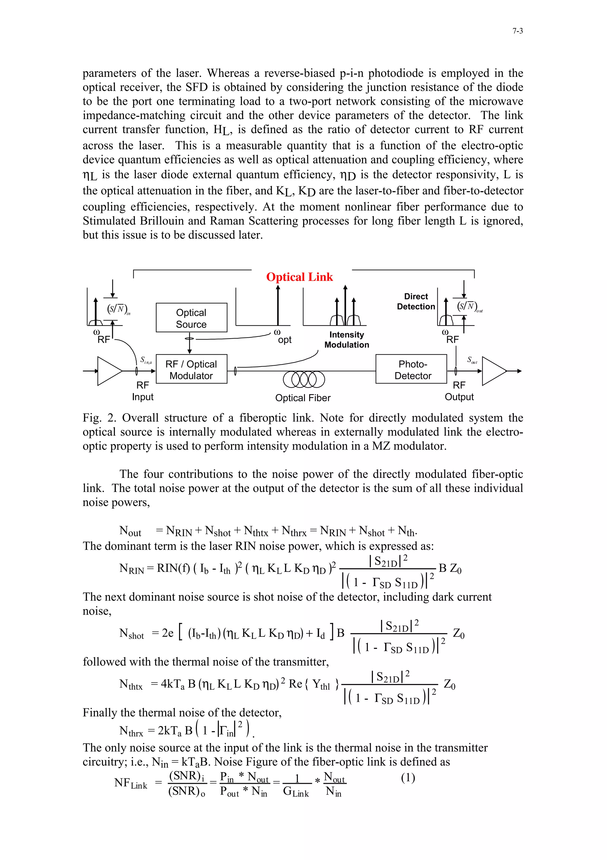
![7-5
40
Gain Predicted
30 By Model
Externally Modulated
20 Solid State Laser
(Vπ = 0.65 V, φ = 90°)
LINK RF Gain (dB)
Measured Gain
Link RF GAIN (dB)
10
0 Directly Modulated High-
Slope-Efficiency Laser
-10
-20
Directly Modulated Low-
Slope-Efficiency Laser
-30
-40
0.001 0.01 0.1 1 10 100
AVERAGE Detector Current (mA)
Average DETECTOR CURRENT (mA)
Fig. 3. Comparison of experimental and simulation results of directly and externally
modulated fiber optic links at HF [2]. (Courtesy of Ed Ackerman of Photonics Inc).
Dynamic Range: Spurious free and compression dynamic range are directly related to
linearity off the optical modulator (i.e., laser diode in the case of directly, and MZ
modulator in the externally modulated FO links). The 3rd order intercept point and 1 dB
compression point for the directly modulated are calculated [1] based on the optical
modulation index m,
2
m2 I - I 2 1 - S22L ΓLas Z0
Pin,int = int b th
2
S21L 2 1 - ΓLas
2
m2 CP Ib - Ith 2 1 - S22L ΓLas Z0
1dB
Pin,1dB CP =
2
S21L 2 1 - ΓLas
In a similar fashion, the 3rd order intercept point and 1 dB compression point are derived
for externally modulated fiberoptic links as:
2
8 Vπ 1 - S22m ΓM
2
Pin,int =
2
π 2 Z0 S21m 2 1 + ΓM
2
0.950454 2 Vπ 1 - S22m ΓM
2
Pin,1dB CP =
2
π 2 Z0 S21m 2 1 + ΓM
Using the derived relationship for intercept and compression points, Spurious Free and
compression dynamic range are calculated using the following expressions:
Pout,int
SFDR = 2 × 10 Log10 dB.Hz2/3
3 kTaG NF
Pout,1dB CP
CFDR = 10 Log10 dB.Hz
kTaG NF](https://image.slidesharecdn.com/en-028-all-120926115440-phpapp01/75/En-028-all-123-2048.jpg)
![7-6
Fig. 4 represents the calculated dynamic range of externally and directly
modulated fiberoptic links as a function of frequency and makes comparison against the
measured results at various operating frequencies. Moreover, references are made to
various practical military and civilian applications at those frequency bands. As seen the
externally modulated fiber optic link with high power and low RIN noise solid state laser
as source combined with high power handling photodetectors provide for the highest
dynamic range. However, note that at lower frequencies, externally modulated link using
DFB lasers as source outperforms solid state laser due to its RIN resonance peak about
MHz. In the directly modulated links, a higher dynamic range is obtained in DFB laser
based systems where a lower RIN noise is obtained compared to FP laser diodes.
On the other hand, Fig. 5 compares cost vs DR performance of directly and
externally modulated links reported. The dashed line corresponds to the current cost-
performance limit of the reported FO links. In addition a number of civilian applications
are identified in this figure. As indicated, even though externally mdulated links will
meet the stringent requirements of many commercial applications, however due to its
high-cost can not be considered economically viable. Therefore, the derive needs to be
either improving performance of directly modulated links or through manufacturing
innovations drive the price of externally modulated links down.
1 dB Compression Dynamic Range
160
Standard External Modulator
150 Diode Laser
140
Dynamic Range (dB-1 Hz)
Two-Tone, Third-Order Microcells
130 Intermodulation-Free Dynamic Range (Outdoor)
DFB Laser
120 L S X Radar Bands
CATV
G G G
Standard External Modulator E
110 B E
G B
Fabry-Perot (FP) Laser:
Extreme Scatter in Experimental Data;
100 Maximum Performance Approaches DFB
90 J
Experimental Data Points
External Direct
Standard MZ Gray Boxes = Specifications
80 DFB
FP Picocells
70 (Indoor)
Lines Indicate General Trends
60
0.01 0.1 1 10 100
Fig. 4. Comparison of measured and calculated dynamic range for directly and externally
modulated fiber optic links [2]. (Coustesy of Ed. Ackerman of Photonics Inc.)](https://image.slidesharecdn.com/en-028-all-120926115440-phpapp01/75/En-028-all-124-2048.jpg)
![7-7
100k External Modulator
(RIN=-160dB/Hz, IM3=-80dBc)
DFB
Laser Diode
Transmitter Cost (a.u.)
(RIN=-150dB/Hz, IM3=-80dBc)
10k Analog Cellular, PHS, PDC
Fabry-Perot
Laser Diode
(RIN=-135dB/Hz, IM3=-60dBc)
CATV
(Down Link)
1k
PCS (CDMA)
100
CATV
(Return Link) PCS (TDMA)
Wireless LAN
(SS)
10
80 100 120
Spurious Free Dynamic Range (dBHz 2/3)
Fig. 5. Cost-Dynamic Range comparison of directly and externally modulated fiber optic
links for a variety of civilian applications [3].
Fiber Nonlinearity: WDM optical systems are employed in optically controlled phased
array antenna applications, where long length of optical fibers are employed for true time
delay devices in large apertures. In pushing these systems to the limits of transmission
capability, aspects such as fiber nonlinearities need to be understood. These aspects
include the nonlinear fiber phenomena of SRS (stimulated Raman scattering) [4], SBS
(stimulated Brillouin scattering) [5], and XPM (cross phase modulation) [6]. These
nonlinear effects become noticeable particularly in WDM subcarrier multiplexed (SCM)
systems that may cover a lot of closely packed video channels cover long distances.
These nonlinearities result in optical power transfer to higher and lower optical
frequencies. Each nonlinear effect creates a distortion level that becomes intolerable
above the acceptable threshold level. Threshold requirements are based on electrical
nonlinear distortion requirements, composite second order (CSO) and composite triple
beat (CTB) (particularly CTB), which have been determined in published works such as
[8, 9].
Fig. 6 shows the SRS crosstalk level for a two channel WDM system, while the
fiber length is varied and for 9.4 nm channel spacing, an input power of 4 dBm, a
dispersion of 17 ps/nm/km, and a subcarrier frequency of 152 MHz. The two curves in
the figure represent the high and low dispersion fibers. The more dispersive fiber
generates lower XT due to the walk-off effect. As is expected, the crosstalk level begins
to increase as the fiber length increases. However, the XT level reaches a peak value and
then decreases as the length is increased further. As the length is increased beyond 70
km, eventually the SRS level reaches a steady state value. This behavior shows a
sinusoidal dependence of crosstalk on fiber length for dispersive fiber but a monotonic
increase in for the dispersion shifted fiber. The importance of this result is that due to the
walk-off effect, the crosstalk level for a length of fiber may not increase as the fiber
length increases. Hence, the crosstalk level can be reduced or increased depending upon
the fiber length. In comparison of the measurement and simulation (based on Wang [8]
and Phillips [9] models), the maximum error is less than 5 %. Measurement results of the](https://image.slidesharecdn.com/en-028-all-120926115440-phpapp01/75/En-028-all-125-2048.jpg)
![7-8
SRS crosstalk while increasing the RF frequency from 50 to 725 MHz in steps of 50
MHz is depicted in Fig. 7. Also included in the figure is a simulation of the Phillips
model [9]. Figure 7 shows that as the frequency is increased, the SRS crosstalk level
changes following a behavior similar to a sinc function [i.e., sinx/x] squared fashion.
-55
2.7 ps/nm/km
-60
-65
17 ps/nm/km
-70
-75
Model 1
-80 Model 1
Measured
-85
0 20 40 60 80 100
Fiber Length (km)
Fig. 6 Measured and simulated SRS induced crosstalk versus fiber length for an input
optical power level of 4 dBm, fiber dispersion of 17 ps/nm/km, RF frequency of 151.85
MHz, and a channel spacing of 9.4 nm.
-53
-56 Model 2 (20 km)
Measured (20 km)
-59 Model 1 (20 km)
-62 Model 2 (40 km)
-65
-68
-71
-74
-77
-80
0 50 100 150 200 250 300 350 400 450 500 550 600 650 700 750
Frequency (MHz) .
Fig. 7 Measured and simulated SRS crosstalk versus RF frequency with a fiber length of
20 km, fiber dispersion of 17 ps/nm/km, channel spacing of 9.4 nm, and a 4 dBm (2.5
mW) input power per channel, also a simulation of 40 km using only the Phillips model.
The problem of crosstalk becomes more aggravated as the number dense WDM
channels increases. Even though analytical models were developed by Wang [8] to
address N optical channels, but there are certain deficiencies associated with this model.
An “alternative technique” was used to predict that for an 8 channel system, the crosstalk
level could easily violate the acceptable cross talk. Specifically, for an input power of – 4
dBm, a subcarrier frequency of 50 MHz, a channel spacing of 1.6 nm (λ8 = 1541.4 and
∆λ = 11.2 nm), and a fiber length of 40 km, the – 65 dBc threshold is violated. However,](https://image.slidesharecdn.com/en-028-all-120926115440-phpapp01/75/En-028-all-126-2048.jpg)
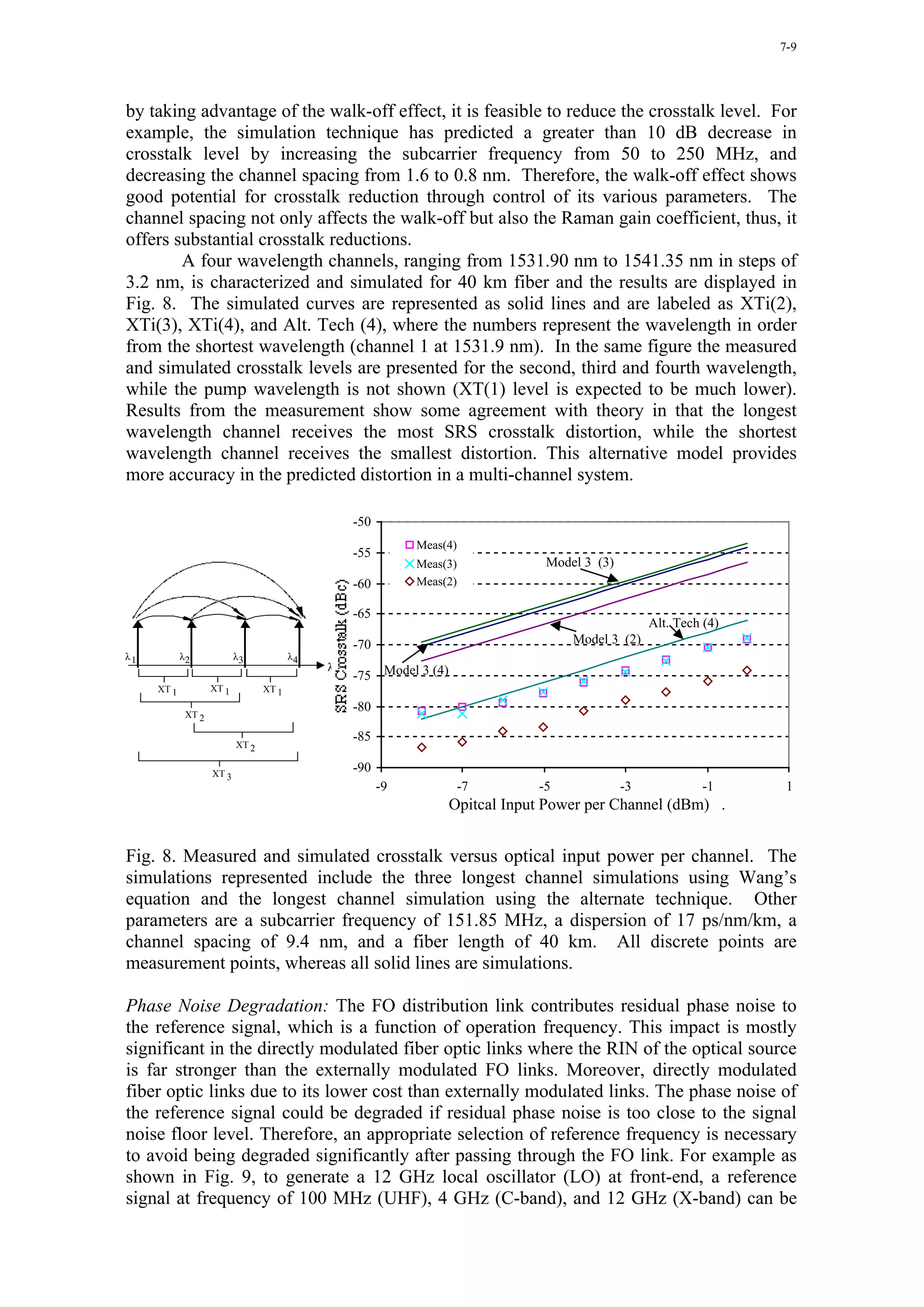
![7-10
sent through FO link. Since the phase noise contributions for FO links are different at
these frequencies, an optimum frequency for reference signal can be found to have the
least phase noise degradation due to FO link.
The optical spectra of a modulated optical signal are expressed as:
Popt 1 + m cos ωm t + δφm (t) + nRIN (t) cos ωopt t + φopt (t) + δφopt (t) , where Popt is the
averaged optical power, m is the optical modulation index at modulating microwave
carrier, ωm. The focus of present work is δφm, the residual phase noise added to the
microwave carrier from the laser diode noise source. nRIN is the relative intensity noise;
ωopt is the optical frequency; φopt is the optical phase signal due to side modes and
modulation, and δφopt is the phase noise of the optical signal. Since most fiber-optic links
for antenna remoting applications use intensity detection, only the noise signals in optical
intensity affect the microwave carrier signal, namely, δφm and nRIN. The nRIN could
contribute to the FM noise of the reference signal through nonlinear AM/PM conversion
[10].
Reference Frequency Reference Frequency
Alternatives Generation
100 MHz
Microwave or
X40
UHF MMW Generation
Fiber Optic Link
4 GHz
Microwave or
Tx Rx
C-Band MMW Generation
Reference
12 GHz Microwave or
X-Band MMW Generation
Fig. 9. Distribution of frequency reference and generation of MMW signal using various
frequency references used in a FO based local oscillator (LO) synchronization network.
The laser diode SSB phase noise of the nth harmonic of the modulating signal,
£out, has contributions from three noise terms: i) the input reference signal phase noise,
£in; ii) the low frequency noise of laser diode up-converted to the carrier frequency, £up;
and iii) the RIN noise at the offset microwave carrier, £RIN. This behavior is quite
analogous to microwave systems [11]. Therefore at angular offset carrier frequency of Ω,
£out can be approximately expressed as [12]:
£out,n ω(Ω) = n2 £in, ω(Ω) + n2 £up, ω(Ω) + £RIN,n ω(Ω) (2)
The factor of n is the harmonic order of the modulation signal, if any nonlinearity of laser
diode is exploited to generate the nth harmonic [10]. (If the fundamental frequency is
employed then n=1.) The subscript ω indicates the modulation frequency. The up-
conversion factor of low frequency RIN to phase noise is the dominant noise source. The
calculation of this up-conversion factor depends on the derivative of the RF phase with
respect to the RF derive amplitude and is Cup, ω = 1/2(∂θ(ω)/∂Po )2 P2 , which θ is phase of
o
optical signal at the modulating frequency ω. The dependence of phase on the optical
output power in directly modulated system is a bit more complicated than externally
modulated system since the nonlinear behavior is dependent on modulation index of laser](https://image.slidesharecdn.com/en-028-all-120926115440-phpapp01/75/En-028-all-128-2048.jpg)
![7-11
diode and relationship of its operation frequency compared to the relaxation oscillation
frequency. This process is nonlinear and at certain frequencies results in AM-PM
compression. The results are related to modulation index through “a” parameter, which is
a function of modulation frequency and averaged optical power [1].
Since in semiconductor laser diodes RIN noise are strong up to 100 MHz because
of mode partition noise, it is predicted that the spectral purity of the UHF reference signal
is greatly degraded, resulting in a higher FM noise. Moreover, the X-band modulating
signal is close to the relaxation oscillation frequency where RIN is peaked. The best
frequency for reference signal distribution through DMFO link is the C-Band signal as
depicted in Fig. 10, where the phase noise of the 12 GHz LO signal is generated from the
reference signal through the above mentioned DMFO link. Clearly, the signal generated
from a C-band signal has the best phase noise performance. The signal from UHF
reference degrades greatly because the residual phase noise of the FO link is higher than
the reference phase noise at offset frequency higher than 100 Hz.
-2 0
From 100MHz ref.
From 4GHz ref.
-4 0
From 12GHz ref.
-6 0 Ref. @100MHz
Phase Nose (dBc/Hz)
Ref. @4GHz
-8 0 Ref. @12GHz
-10 0 FO Noise @ 12GHz
-12 0
FO Noise @ 100MHz
-14 0
-16 0
FO Noise @ 4GHz
-18 0
-1 0 1 2 3 4 5 6
10 10 10 10 10 10 10 10
Offset Frequency (Hz)
Fig. 10. The simulated phase noise of a LO signal at 12 GHz, which is generated from
different reference signals through a directly modulated FO link as depicted in Fig. 9.
3.0. Semiconductor Laser Diodes with Self-Resonance
It is attractive to achieve optical systems that provide a performance analogous to
the electrical functions. For example, a laser source with oscillation at millimeter wave
frequencies along with the opto-electronic mixing would resemble the SOM circuit. A F-
P laser with optical feedback has provided this feature and was first reported by Lau [13].
This resonance frequency is stabilized using a modulating frequency fundamentally or
harmonically related to the self-resonance frequency. A thorough characterization and
explanation of FM noise degradation of the frequency reference in the laser is also
reported by Ni et al [12].
A monolithic version of laser with external cavity is realizable using semiconductor
fabrication process and reported by a number of researchers. Fig. 11a shows a schematic
drawing of the monolithic laser with an integrated EA modulator. Stacked structure
consisting of two MQW layers, a MQW for laser diode (MQW-LD) and a MQW for EA](https://image.slidesharecdn.com/en-028-all-120926115440-phpapp01/75/En-028-all-129-2048.jpg)
![7-12
modulator (MQW-MD) are employed. The F-P cavity length for our experiment is
cleaved approximately for a length of 2170µm. This total length is composed of 1970 µm
long gain section, 150 µm long modulator, and a 50 µm long separation region. The facet
of the modulator section is coated with high reflective film (R≈85%). The facet of the
gain section is as cleaved. The laser is mounted in a high-frequency package. The
schematic diagram of the long FP laser with integrated EA modulator is shown in Fig.
11b.
The gain section of the laser diode is forward biased at different bias currents and
the EA section is reverse-biased by different voltage levels. The natural frequency
response of the laser is measured at various laser bias currents, ranging from Ib=80mA up
to Ib=150mA for bias voltage of Vm=0V. A resonance peak is observed that is associated
with the longitudinal mode separation in the long FP laser. The longitudinal mode
separation is calculated as ∆f=c/2nL≈19.3GHz, where c=300mm.GHz is speed of light in
free space, n≈3.5 is index of refraction of wave-guide, and L≈2.17mm is the F-P cavity
length. This resonant frequency has a frequency tuning sensitivity of ≈1MHz/mA.
One could stabilize the optical oscillations using injection-locking process as
demonstrated [13]. As the gain section is modulated by a synthesized frequency reference
(HP83640A) of Pm≈-1dBm at fm=19.258GHz, a single oscillation peak appears. The
familiar one-sided injection-locking spectra are observed outside the injection locking
range and the close-in to carrier phase noise is significantly reduced within the locking
range. The measured close in to carrier phase noise degradation at 100Hz offset carrier is
depicted in Fig. 12, where 31dB and 6dB degradation are measured for the injected
power of Pm=+0.5dBm in the resistively- and reactively-matched modules respectively.
However for injected power level of +4.5dBm, a close-in to carrier phase noise identical
to the reference source is measured for the reactively-matched case.
Reference Signal Bias Current
(Mode-Locked) Isolation Data Signal
EAModulator GainSection Section
150µm 50µm 1970µm
p-InGaAsP
Reference Signal
P-InP M -LD
QW (Injection-Locked)
HR InP EA Gain
n-InP Modulator Section
MW D
Q -M Section
(a)
(b)
Fig. 11. a) Conceptual representation of the long F-P laser integrated with an electro-
absorption modulator; b) mechanical fixture used for mounting of the laser diode for
injection locking, mode locking and opto-electronic conversion evaluations.
The 19.3 GHz resonant frequency has a frequency tuning sensitivity of
≈1MHz/mA. The resonance frequency is stabilized using fundamental mode-locking by
modulating the EA section by a synthesized source. The close-in to carrier phase noise
are measured and comparison is made against the reference signal from an HP83640A
source. The results are summarized in Table I for different laser operation points. As
indicated a very small phase noise degradation is observed, however the results for Vm= –
1 V is better that the results for Vm =-4.5V for the same laser current of Ib=140mA.](https://image.slidesharecdn.com/en-028-all-120926115440-phpapp01/75/En-028-all-130-2048.jpg)
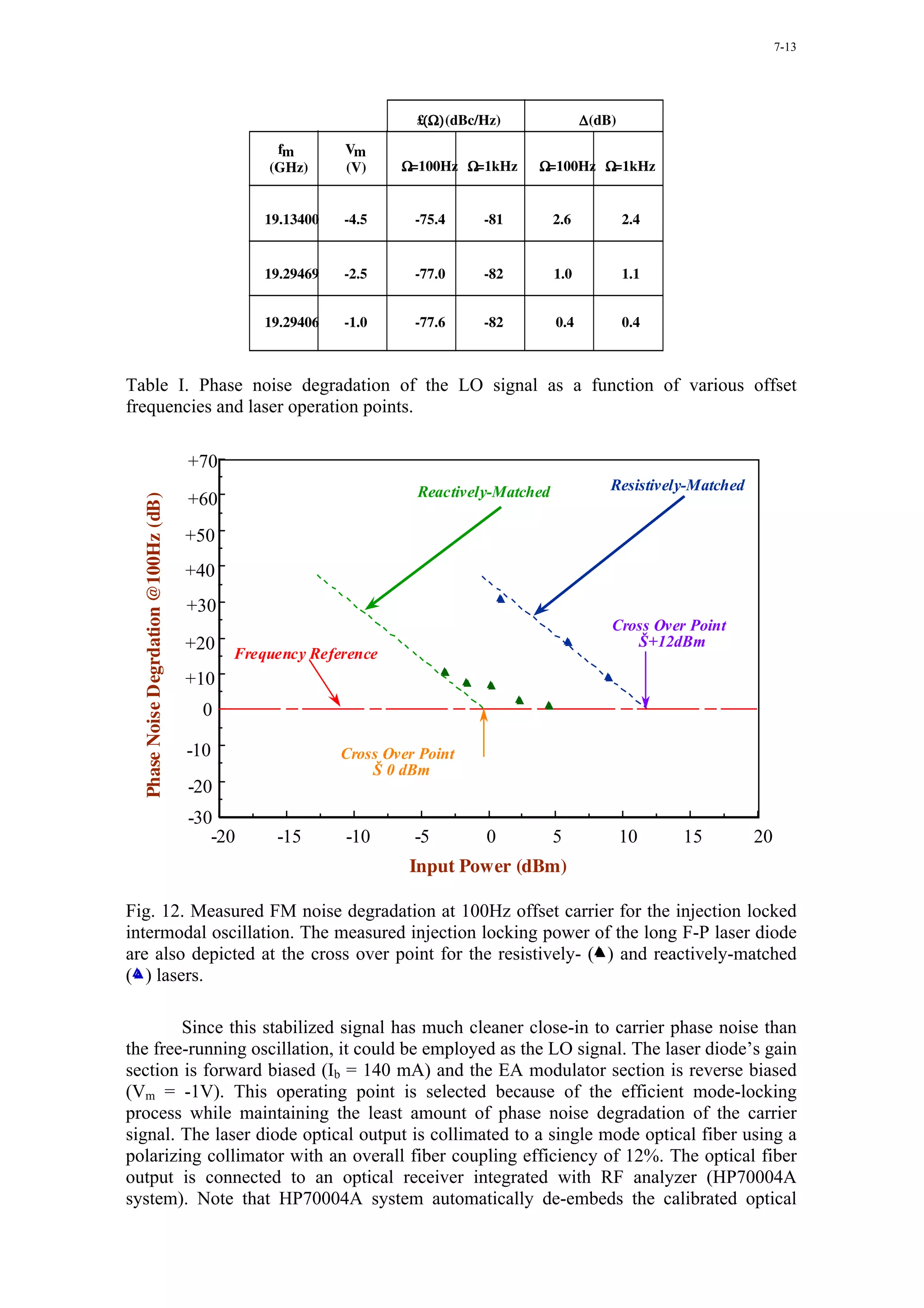
![7-14
receiver response from the measurement and displays it in the optical domain. The
electrical domain power levels, in dBr, are easily calculated by multiplying the depicted
optical domain results, displayed in dBm, by a factor of 2.
Next the gain section of this laser is modulated by S-band signals (2.2 GHz ± 50
MHz). Strong nonlinearity of the mode-locked laser at the LO signal of 19.3 GHz up-
converts the S-band signals to 17.1 GHz and 22.5 GHz as shown in Fig. 13. The data
modulation power level is changed over a wide range. An optical conversion loss is
defined as the ratio of the generated mixed RF signal (19.3 ± 2.2 GHz) to the IF signal
(2.2 GHz). The optical conversion loss is as low as 1.4 dB resulting in the electrical
conversion loss of 2.8 dB. The opto-electronic conversion loss for the lower side-band
(LSB) at 17.1 GHz is higher than the upper side-band (USB) of 22.5 GHz by 1.3 dB (i.e.,
2.6 dB electrical) [14].
On the other hand, a modulation loss greater than 51 dB is measured when the
gain section is directly modulated by the RF signal at 17.1 GHz. The spurious-free
dynamic range (SFDR) of this opto-electronic mixer is also evaluated. The
intermodulation distortion (IMD) measurements are conducted for two modulating tones
which are 5 MHz apart (e.g., f1 = 2.200 GHz and f2 = 2.205 GHz). Both tones are up-
converted by stable LO signal of 19.360 GHz and IMD of the up-converted RF signals
are measured at LSB and USB frequencies. Based on the mode-locked laser IMD and
RIN noise measurement results for the up-converted RF tones, SFDR LSB and USB RF
signals are ≈ 88 dB.Hz2/3 and 89 dB.Hz2/3 respectively.
5
Normalized Light Output Power (dB)
fm
-5
fs
fm+f s
Carrier
2f m
-15 2f m+fs
fm-f s
RF Signal 2f m-f s
fm-2f s fm+2f s
IF Signal
40 50
Frequency (GHz)
(a) (b)
Fig. 13. Opto-electronic mixing of data signal with local oscillator signal in the
mode-locked long FP laser diode. a) Experimental results for the operating condition is
Ib = 140 mA, Vm = -1 V, fm = 19.360 GHz, Pm = +15 dBm, fdata = 2.200 GHz, and Pdata = -
25 dBm. Data, lower side-band RF, and local oscillator signals (center frequency of 11.0
GHz and frequency span of 20.0 GHz); b) simualtion results based on travelling wave
rate equation [15].
4.0. CONCLUSIONS
Fiber fed wireless communication is considered for mobile and fixed-point
communications in micro and pico-cellular as well as many military ad-hoc WLAN
scenarios. This paper has addressed fiber optic distribution of analog data in terms of link
gain and dynamic range and frequency reference signal for generation of a coherent local
oscillator signal in terms of AM/PM conversion. Moreover, distortion induced by SRS in](https://image.slidesharecdn.com/en-028-all-120926115440-phpapp01/75/En-028-all-132-2048.jpg)
![7-15
dense WDM systems is discussed. Fiber optic links based on directly modulated could
meet cost-performance for many applications, even though monolithically integrated EA
modulators are becoming very attractive. (This topic is discussed in a paper in this
proceedings dealing with the state-of the-art of devices and circuits by Prof. Dieter
Jaeger.)
A monolithically integrated FP laser with EA modulator is employed to
simultaneously transmit frequency reference of data signals. The analytical models
indicate that stabilized LO signal at 19.3 GHz can be attained using injection locking and
mode-locking. The achieved close-in to carrier phase noise of the stabilized LO signal is
lower in the case of injection locking than mode-locking for the same modulating power
level. The opto-electronic mixing of 19.2 GHz LO and S-band data is also feasible using
this device with SFDR as high as 90 dB. Hz2/3. Moreover, optoelectrnic mixing can occur
in a mode-locked laser, creating possibility of generating RF signal from frequency
reference and data signals, thus bypassing the need for integration with electrical mixers
in the up- and down-conversion. (A similar approach using attractive microchip laser is
presented in this proceedings by Prof. Tibor Berceli.)
ACKNOWLEDGMENT
The author wishes to acknowledge the contribution of many of his students,
partciularly Dr. Edward Ackerman, Mr. Adam McInvale, Dr. Tsang Der Ni, Dr.
Xiangdong Zhang, and Dr. Joong Hee Lee.
REFERENCES
[1] A. S. Daryoush, E. Ackerman, N. Samant, D. Kasemsat, S. Wanuga, "Interfaces for
High-Speed Fiber Optic Links: Analysis and experiment," IEEE Trans. on Microwave
Theory and Techniques, vol. 39, no. 12, Dec. 1991.
[2] Edward Ackerman, Photonics Inc., Private Communications.
[3] K. Emura, “Technological Choices in Optical Fiber Feeding Wireless Access
Systems,” Microwave Photonics Satellite Workshop, Dec. 1996, Kyoto, Japan.
[4] A.R. Chraplyvy, P. S. Henry, "Performance degradation due to stimulated Raman
scattering in wavelength-division-multiplexed optical-fiber systems," Electron Lett., Vol.
19, No 16, August 1983.
[5] A.R. Chraplyvy, “Limitations on Lightwave Communications Imposed by Optical-
Fiber Nonlinearities,” J. of Lightwave Technology, Vol. 8, No. 10, Oct. 1990.
[6] Z. Wang, et. al., “Effects of Cross Phase Modulation in Wavelength SCM Video
Transmission Systems,” Electronics Lett., Vol. 31, No. 18, August 1995.
[7] T. E. Darcie et. al., “Lightwave Multi-channel Analog AM Video Distribution
Systems,”IEEE International Conference on Communications, Boston, MA, June 1989.
[8] Z. Wang, A. Li, C.J. Mahon, G. Jacobsen, and E. Bodtker "Performance Limitations
imposed by Stimulated Raman Scattering in Optical WDM SCM Video Distribution
Systems", IEEE Photonics Techn. Lett., Vol. 7, No. 12, December 1995.
[9] M.R. Phillips and D.M. Ott, “Crosstalk Due to Optical Fiber Nonlinearities in WDM
CATV Lightwave Systems,” J. of Lightwave Technology, Vol. 17, No. 10, Oct. 1999.
[10] X. Zhang, T.D. Ni, and A.S. Daryoush, “Laser Induced Phase Noise in Optically
Injection Locked Oscillator,” Digest of IEEE 1992 MTT Symposium, pp.765-768, 1992.
[11] X. Zhang and A.S. Daryoush, "Bias Dependent Low Frequency Noise Up-
Conversion in HBT Oscillators", IEEE Microwave and Guided wave Letters, vol. 4, no.
12, pp. 423-425, Dec. 1994.
[12] T.D. Ni, X. Zhang, and A.S. Daryoush, "Experimental Study on Close-in carrier
Phase Noise of Laser Diode with Coherent Feedback," IEEE Trans. Microwave Theory
and Techniques, vol. 43, no. 9, pp. 2277-2283, Sept. 1995.](https://image.slidesharecdn.com/en-028-all-120926115440-phpapp01/75/En-028-all-133-2048.jpg)
![7-16
[13] K. Lau, “Short-Pulse and High-frequency Signal Generation in Semiconductor
Lasers,” IEEE Journal of Lightwave Technology, Vol. 7, No. 2, pp. 400-419, Feb. 1989.
[14] A.S. Daryoush, K. Sato, K. Horikawa, and H. Ogawa, “Efficient Opto-electronic
Mixing at Ka-Band using a Mode-locked Laser,” IEEE Microwave and Guided Wave
Lett., vol. 9, no. 8, pp. 317-319, August 1999.
[15] A. S. Daryoush, et al., “Applications of Opto-Electronic Mixing in Distributed
Systems” Digest of 2001 Topical Symposium on Millimeter Wave, TSMMW2001,
Yokosuka, Japan, pp. 175 – 178, March 2001.](https://image.slidesharecdn.com/en-028-all-120926115440-phpapp01/75/En-028-all-134-2048.jpg)
![8-2
have been demonstrated in the last twenty years, such as OCO and optically tuned filters
[1], phase shifter [2], amplifiers [3], switches[4], and antennas [5]. Even though these
techniques are intriguing, but have not found significant applications yet. More recently,
spurred by rapid developments in fiberoptic based networks (MAN and LAN), the chip
level integration of photonic and microwave components for high performance optical
receivers have gained attention. PIN-amplifier configurations, such as PIN-HEMT [6]
have been reported, and lately high performance PIN -HBT combinations have been
realized by Aitken et. al. [7]. The three terminal microwave devices are attractive to
perform photodetection and control functions in the receiver front-end [8, 9]. This
configuration enhances receiver performance by reducing parasitics, requires less pre-
amplification due to intrinsic gain of transistors, and has lower power consumption and
less costly fabrication.
The key to these developments and related applications in communications and
control of microwave systems is the understanding of the optical properties of microwave
devices. Professors Seeds and Salles provided an excellent overview on this topic in 1990
[10]; however, since then the developments of HBT have brought more emphasis on the
subject. Particularly photo-response of HBT, MESFET and HEMT could be unified and a
comparison is made in terms of inherent photo-detection mechanism, gain, sensitivity,
and bandwidth.
Static Analysis: Table I summarizes various effects that contributes to the photoresponse
of the HBT, MESFET, HEMT, and its comparison to PIN photodiode. (The performance
of PIN photodiode is considered as baseline.) For PIN photodiode the photoresponse
current is determined by the photo-generated electron-holes pairs in the intrinsic region
and no current gain is experienced. The light level directly controls the photocurrent in a
linear fashion. On the other hand in HBT, in addition to photo-generated electrons at the
collector depletion region, there is an increase in the effective base current due to the drift
of photogenerated holes from the collector depletion region to the base. This source of
this term is change in current injection rate due to change in base voltage and hence is
labeled as internal photoconductive effect; since this increase occurs under constant bias
current, it results in current gain. The photoresponse of the HBT is linear with optical
power.
Ipvi Ipvx Ipc Ipci Ipd
gain speed gain speed gain speed gain speed gain speed
PIN ----- ------ ------ ------ ----- ----- ------ ------ none very
- fast
HBT ----- ------ ------ ------ ----- ----- moderate fast none very
- (linear) fast
FET large slow large very small fast ------ ------ ------ ------
(log) (log) slow
HEMT large slow large very small fast ------ ------ ------ ------
(log) (log) slow
Table I . Sources of photo-detection mechanisms in popular microwave semiconductor
transistors and their comparison to PIN photodiode as baseline.](https://image.slidesharecdn.com/en-028-all-120926115440-phpapp01/75/En-028-all-136-2048.jpg)
![8-3
On the other hand, the photoresponse in both field effect transistors (MESFET and
HEMT) is attributed to three mechanisms [11]. The photogenerated carriers collected at
the gate yield a photovoltage Vphx, when passing through an external resistor. Thus the
external photovoltaic increases in gate bias, which opens the channel and results in a
photocurrent of Ipvx = gm Vphx. The internal photovoltaic effect results in Ipvi = gm Vph,
where for MESFET [12] Vph is a light-induced modulation of the channel height and in
the case of the HEMT, Vph represents a shift in the quasi-Fermi level [13]. The
photoconductive effects Ipc are very small, and are neglected. The optical responsivity of
microwave semiconductor transistors is compared in Fig. 1. At low illumination the
logarithmic response of FET devices provides large gain. However, photoresponse
saturates rapidly, which limits their dynamic range. The HBT, which has relatively large
dark current, but low noise [14], performs best at moderate and high illuminations.
100000
MESFET
10000
1000
HEMT
(A/W) 100
HBT
10
1 PIN
0.1
1E-04 1E-03 1E-02 1E-01 1E+00 1E+01
Optical Power (mW)
Fig. 2 Comparison of the static light responsivity for microwave transistors and their
performance comparison to PIN Photodiode as a baseline. (Courtesy of Prof. P.R.
Herczfeld of Drexel Univ.)
Dynamic Response: The frequency response of a PIN is limited by the carrier transit
time, where a shorter intrinsic region yield a faster response but this behavior is at the
expense of quantum efficiency for vertical devices. (Traveling wave photodiodes are
designed to simultaneously meet high power handling, speed, and efficiency
requirements.) The speed of the HBT is governed by sum of different time constants
associated with the charging time of the B-E junction, the base transit time, the charging
time of the B-C junction, and the transit time across the collector depletion region. The
optical response of the HBT is fast since these time constants are the same as those which
determine the HBT ultra high-speed response. Whereas for the FET devices the external
photovoltaic effect is very slow because of the long charging time of the gate external
circuit. The MESFET’s dynamic response is dominated by the dynamics of the internal
photovoltaic effect, which is defined by the RC time constant of substrate resistance and](https://image.slidesharecdn.com/en-028-all-120926115440-phpapp01/75/En-028-all-137-2048.jpg)
![8-4
the epi-layer/substrate junction capacitance [14]. For the HEMT, on the other hand, the
RC time constant, determined by the buffer resistance and the change in electron
concentration in the 2-DEG channel [12], defines the speed. It is important to note that
the speed of photoresponse of the FETs is independent of their microwave speed.
The measured and calculated frequency response for these devices is depicted in
Fig. 2. At low frequencies FETs perform well, but the intrinsically slow photovoltaic
effect yields a small gain-bandwidth product. The speed of the HBT and PIN is
comparable. Note, increasing the coupling of efficiency of the HBT from 1% to 10%,
which is a feasible task, will reduce the link insertion loss by 20dB, and thus supersedes
that of the PIN. Using devices with larger β (e.g. 250 instead of 25) will also give
additional advantage to the HBT.
Recent publication on nonlinear behavior of high-temperature superconducting
film as photomixer has provided opportunity to generate THz signals using the kinetic
inductive photoresponse [15]. These new applications maintain interest in light
interaction with microwave circuits.
0
MESFET
-10 &
electric characteristics - 1/ τ ec
HEMT
-20
-30 PIN
-40
ain (dB) HBT
-50
-60
-70
HEMT
photoconductive response
-80 cut-off
-90
1 10 100 1000 10000 100000
Frequency (MHz)
Fig. 2. Frequency response of microwave devices, measured data is represented by
discrete points and theory by solid lines. The optical coupling efficiencies were
calculated to be less than 1% for the HBT, 4% for the MESFET and the HEMT and 60%
for the PIN. (Courtesy of Prof. P.R. Herczfeld of Drexel Univ.)](https://image.slidesharecdn.com/en-028-all-120926115440-phpapp01/75/En-028-all-138-2048.jpg)
![8-5
3. Optical ADC Techniques
Optoelectronic devices have demonstrated ultra-fast switching speed and mode-
locked lasers have achieved high-speed and accurate optical pulses. With capability of
sampling electrical signals at resolutions of sub-picoseconds, implementation of optical
Analog-to-Digital Converter has long intrigued many researchers due to it s following
advantages. Since optical sampling has time jitter that is about 2 orders lower than
electronic clock. Second, optical sampling decouples sampling electrical signal and
sampled optical signals. Third, optical sampled or quantized signal is easy to distribute by
fiber and remotely controlled. Also, many photonic ADC approaches also produce output
as Gray-codes directly, eliminating the need for additional encoding circuits. However
optical quantization is generally limited to resolution of a few bits and this remains a big
challenge. There are two approaches to quantize the information after sampling by optical
signal: i) hybrid optic-electronic ADC, where electrical quantizers are employed; and ii)
all-optical ADC, where optical quantization is implemented.
Hybrid optic-electronic ADC: Hybrid optic-electronic ADC, or called optically assistant
ADC, employs optical sampling followed by electronic quantization. It attempts to
combines advantages of both optical and electronic ADC technologies: high-speed rate of
optical sampling and high resolution of electronic quantization. But the speed of
electronic devices is much lower than the optical sampling rate. So the sampled optical
signal has to be down converted to lower speed and channeled to parallel electronic
quantizers. For example, 100 GSPS sampled pulses can be split into 8 channels in time
domain, and the pulse rate in every channel is 12.5 GSPS. Most optical sampling
transducers are implemented with Mach-Zehnder modulators [16], where the output
intensity of the Mach-Zehnder interferometer is function of the applied voltage:
ϕ πV
I out = I i cos 2 ( 0 − )
2 2Vπ
where ϕ0=2πnL/λ0, the optical distance of a branch, and Vπ is the half-wave voltage,
defined as the applied voltage at which the phase shift changes by π. Optical sampling
operates in a small range around Vπ, the output is approximately linearly proportional to
applied voltage V. To extend the linear range of Mach-Zehnder modulator, a number of
linearization approaches were demonstrated. In photonic ADC, the linearization can be
implemented in digital domain by directly inverting the transfer function in DSP.
The key issue in hybrid opto-electronic ADC is to channelize high speed sampled
optical pulses and ensure channels matching in amplitude and time. Based on approaches
of channelization, three major schemes are proposed as: a) time interleaving [17], b)
WDM channelized [18], c) time stretched [19]. The optical sampling and time
interleaving is employed by Juodawlkis et al to implement an ADC with bandwidth up to
505 MSPS by using 1:8 optical demultiplexers and 14-bit electrical quantizers. A dual-
output LiNbO3 MZ modulator is used for linearization processing and a 65 dB SFDR and
47 dB SNR, corresponding to an effective resolution of 7.5 bits. The sampled optical
pulses are split into 8 channels by optical time division demultiplexers, which are
composed of 3 stages of 1×2 switches controlled by 505 MHz driving signals. Therefore
the 16 parallel high-resolution electronic quantizers are working at 63 MSPS [18]. To
achieve an interleaving SFDR of 80 dB, the converter-to-converter gains must be](https://image.slidesharecdn.com/en-028-all-120926115440-phpapp01/75/En-028-all-139-2048.jpg)
![8-6
matched to ~0.01%, the offset must be matched to ~0.01% of the signal amplitude, and
the converter-to-converter crosstalk must be less than one part in 104.
On the other hand using optical dispersive components, multi-wavelength optical
wave is smeared (for continuous spectrum) or split (for discrete wavelengths) in time,
borrowing concept from WDM communication, the sampled optical signal can be
channelized in both wavelength and time domains. The RF signal is sampled by the
WDM pulses and then channelized by a WDM demultiplexer. Clark et al demonstrated a
100-GSPS photonic ADC based on the time- and wavelength-interleaved scheme [18]
using mode-locked fiber laser (MLFL) that generates 12.5 GHz pulse train, and 100-GHz
sampling optical pulses is obtained by an 8× multiplexer. The pulses propagate through
different fiber delays and attenuators which then are recombined in the WDM. The delay
fibers and attenuators can be adjusted for time matching and amplitude equalizing
respectively. The time interweaved pulse train is then demultiplexed in to 8 channels
according to wavelengths. The resulting parallel pulses are then to be quantized by >12.5
GSPS quantizers, but an 8-bit ADC operating at only 781 MSPS was achieved with SNR
of 22~26 dB, which corresponds to about 4 bits. The resolution of wavelength
channelized ADC is still limited since it faces to similar difficulties as the time
interleaving ADC does. The time uncertainty and amplitude uniformity between channels
are difficult to control.
Bhushan et al demonstrated a record ultra-fast sampling rate of 130 GSPS using
time stretching approach [19]. The idea behind this ADC is similar to wavelength
channelized ADC, but in time stretched RF input signal modulates a broadband optical
continuous wave (CW) other than is sampled by optical pulses with discrete wavelengths.
The detected analog optical signal is sampled and quantized by electronic ADC. Fig. 3
shows a limited time application of time stretch preprocessing, where a passively mode-
locked fiber laser with 20-MHz repetition rate followed by a 17 nm filter is used to
generate broadband short pulses. The optical pulse propagates through a dispersive fiber
of length L1 and dispersed in time to get 0.8 ns time aperture. The wave is then
modulated by RF signal to be converted. The modulated wave is sent to another piece of
dispersive fiber of L2 to be stretched in time domain. The ADC obtain a stretch ration of
M=16.2 by proper choosing L1 and L2, where then the stretched signal is detected and
digitized by a single 8-GSPS electronic ADC of an oscilloscope. So the effective
sampling rate is about 130 GSPS (8GSPS × 16.2) with SNR of 45 dB, corresponding to
7.5 bits of resolution.
On the other hand for continuous signals in time, a parallel architecture must be
used in order to preserve the information. In this process an arrayed waveguide grating
(AWG) is employed to sample a portion of the optical spectrum and since each optical
wavelength corresponds to a different propagation time delay, the filter performs
sampling in time. Then each segment is time stretched by the same factor M prior to
entering a slow electronic ADC, however both time alignment and amplitude in balance
between various arms of are crucial.](https://image.slidesharecdn.com/en-028-all-120926115440-phpapp01/75/En-028-all-140-2048.jpg)
![8-7
BW = fin BW = fin / n
Time
Stretch Digitizer
xn
Time
Stretched Signal
Frequency
Input Electrical
Input electrical signal
Signal Stretched signal
Dispersion BWChirp
Dispersion
SC Time
Modulator
Source PD
Chirped Optical Pulse
Fig. 3. Time limited signal converted by time stretching ADC [19]. (Courtesy of Prof.
Jalali from UCLA)
All-optical ADC: There are quite a few ways
to implement optical quantization, but
probably the best known photonic ADC is
based on by Taylor patent of 1977 [20]; a
revised design called optical folding flash
ADC in 1995 [21]. Fig. 4 shows a block
diagram of a 4-bit optical folding-flash ADC.
The geometrical scaling of Vπ or electrode
length is eliminated by a parallel-serial
combined configuration. This scheme uses
identical electrode length but sets DC bias at
different points on the interferometer transfer
characteristic curve. The resulting transfer
function of MSB-2 and LSB branch is
obtained by multiplying the functions of all
stages at different bias and show doubled
frequency comparing to previous bit. However
this scheme also presents some additional
challenges. First the MSB is susceptible to
high noise because of the slow changing slope
at digital edges. Second, the transit time
limitation is still not eliminated; moreover, the
hardware complexity increases exponentially
in term of interferometer number as 2(b-1)+1 Fig. 4. Optical folding-flash ADC [21].
and it strongly relies on accurate bias. a) various bias points of all optical ADC,
Another way to quantize optical signal b) realization of MZ modulators for
is to exploit variable electro-absorption quantization, c) the received signal levels
semiconductor modulators demonstrated by for each significant bit.
Hayduk et al [22]. The quantization is
achieved using an architecture that relates the](https://image.slidesharecdn.com/en-028-all-120926115440-phpapp01/75/En-028-all-141-2048.jpg)
![8-8
received analog voltage to an optical intensity, which shares the same idea with electronic
flash ADC, in which 2N-1 comparators with different threshold are used. The use of the
passive materials in this flash photonic ADC architecture with no external voltage
requirement makes this module very low power dissipation. The authors claim that the
ADC has potential to operate at more than 100 GSPS combined with resolution as high as
12-14 bits. But this scheme is susceptible to amplitude fluctuation and unbalanced energy
splitting. A similar idea is also employed in all-optical ADC quantization using
photodetectors with different sensitivities [23].
In the two ADC schemes mentioned above, RF signal is sampled and quantized
by optical amplitude. However the amplitude errors are strongly depends on source
fluctuation, device linearity and loss along the optical link. So it is hard to build high
resolution all-optical ADC based on optical amplitude. An all-optical ADC working in
spectrum domain is demonstrated by Zmuda et al [24], as shown in Fig. 5. The input
signal is sampled by a tunable laser and quantized by processor filters with binary
behavior. The output wavelength of the tunable laser is modulated by the applied
electrical field so the electrical amplitude is represented as wavelength in spectrum
domain. The post-sampled light is processed by a parallel optical filter array. If the
spectrum line falls into the pass band, the output is represented as “1”, otherwise a “0”
will be read. Each filter has periodic equally spaced passband and stopband and
organized in a Gray code manner.
Fig. 5. Optical ADC using tunable laser and filters [24].
The major challenges for this scheme are the filter design of sharp transition and tunable
laser. A 4-bit optical ADC using Bragg grating filters and ring cavity tunable laser is
proposed and analyzed. Because of the convergence time limitation of Fabry-Perot
cavity, only 4 bits of resolution can be achieved at 10 Gs/s. And the performance of
Bragg grating filters (Fig. 6) show limited resolution. The authors proposed a folding
circuit to enhance its resolution, where a Mach-Zehnder interferometer performs the
optical folding circuit and first- or second-order linearization circuit corrects the
nonlinear folded signal. So two low resolution ADCs are coupled with the folding circuit
to achieve M+N bits of resolution. The author claimed the ADC would be able to operate
at conversion speeds in excess of 10 GHz with up to 10- to 12-bits of resolution.
However, it is not clear how the upper M-bit ADC achieved the additional 6 to 8 bits. But
it indicates a promising way to perform analog-to-digital in spectrum domain.](https://image.slidesharecdn.com/en-028-all-120926115440-phpapp01/75/En-028-all-142-2048.jpg)
![8-9
Fig. 6. Performance of Bragg grating filters [24].
4. Near IR Optical Spectroscopy
Near Infrared (NIR) spectroscopy is a
new, non-invasive technique to analyze living
tissue. In NIR spectroscopy, the main aim is to
extract the optical properties (absorption and
scattering) of the living tissue. Absorption
information is used to characterize the
concentration of biological chromophores, such as
hemoglobin (in oxy and de-oxy forms), which in
turn indicates the physiological changes in blood.
This approach could be employed for health
monitoring purposes, such as pilot overload in
combat aircrafts. Scattering information provides
information on composition, density, and
organization of tissue structures, such as cells and
sub-cellular organelles [25, 26]. Therefore, NIR
techniques provide information about disease- Fig. 7. Absorption spectrum of Hb
related functional and structural changes. More (deoxy-hemoglobin), HbO2 (oxy-
specifically, it has been shown recently that hemoglobin), and water in the NIR
physiological changes such as ischemia, necrosis region.
and malignant transformation can produce](https://image.slidesharecdn.com/en-028-all-120926115440-phpapp01/75/En-028-all-143-2048.jpg)
![8-10
important perturbations in tissue optical properties [27]. The importance of NIR spectrum
lies in the fact that in this region tissue absorption is much lower than the other parts of
the spectra (see Fig.7). Apart from tissue information content, this region is attractive
since NIR instruments are inexpensive to construct and are easily portable. These features
allow NIR instruments to be an attractive alternative to other techniques, such as MRI.
Moreover, NIR light is not an ionizing radiation; therefore, it can be used as a usual
clinical monitoring of patients in radiation therapy.
The modulated NIR could be employed for greater spatial and temporal
information and could be explained based on the following physical foundation. When
photons enter a turbid (multiply scattering) media, the photons scatter randomly in all
directions, diffuse through the medium, and get absorbed during this diffusion process.
When source detector separation is large enough and scattering is dominating absorption,
diffusion theory is very well suited approximation for photon transport:
1 ∂Φ (r , t )
− D∇ 2 Φ (r , t ) + µ a Φ (r , t ) = S (r , t ),
c ∂t
where Φ is the fluence rate (W / cm 2 ) , c is the speed of light in the tissue, S is the source
term, µ a is the absorption, and D is the diffusion constant, which is related to reduced
′ ′
scattering constant, µ s , by D = 1 (3 ⋅ µ s ) . In an infinite medium for a point source photon
diffusion wave (PDW) can analytically be expressed as:
S exp(ikr )
Φ (r , t ) =
4πD r
where k is the complex wave vector, (i.e., k = k real + ikimag ) and is described as
combination of modulating frequency, diffusion, and absorption coefficients
as: k = − µ a / D + iω /(c ⋅ D) . The back-scattered PDW has phase lag and amplitude
attenuation relative to the source as:
Θ lag (r , ω ) = kimag .r
Aatt (r , ω ) = exp(−k real r ) /(4πDr )
Fig. 8. Normalized amplitude attenuation (left) and phase-shift (right) of photon density
waves as a function of frequency.](https://image.slidesharecdn.com/en-028-all-120926115440-phpapp01/75/En-028-all-144-2048.jpg)
![8-11
Fig. 8 shows the solution of amplitude attenuation and phase-shift of photon
diffuse waves with respect to frequency (up to 1 GHz) for a breast tissue with optical
absorption and scattering coefficients properties of µ a = 0.05cm −1, µ ′ = 10cm −1 . NIR
s
techniques are also being used for brain imaging a seen in Fig. 9 [28, 29]. The image on
the left is BOLD image from MRI. The image on the right is obtained from diffuse
optical tomography.
Fig. 9. Brain activation image. MRI image is shown on the left and the image from
diffuse optical tomography is depicted on right. (Courtesy of Prof. Britton Chance of
Univ. of Pennsylvania.)
NIR technique uses constant wave (CW), time-domain, and frequency domain
instruments according to their applications and information content. The CW systems are
very inexpensive, however suffers from limited resolution. Frequency domain
instruments are more compact, cheaper, and algorithms are easier to handle than time-
domain techniques, hence frequency-domain instruments are more attractive. In
frequency-domain photon migration concept is easier too. When light is modulated with
modulation frequencies in megahertz region, diffuse photon density waves (PDW) are
generated, propagating with a wavelength of several centimeters [30-33]. At the detector
one measures the amplitude decay and phase shift data of these waves (see Fig. 8).
Amplitude and phase data are used to map the optical absorption and scattering properties
of the medium. Optical constants in turn are used to obtain hemoglobin concentration,
blood volume and oxygen saturation. More accuracy of the extracted results is achieved
when a frequency swept mode is employed, and as the modulation frequency increases to
microwave region a higher spatial resolution is attained.
5. Tunable Microchip Lasers
Compact, efficient solid-state microchip lasers, with high spectral quality, show
great potential as optical transmitters for rapidly tunable sub-carrier sources in
biomedical imaging and hybrid lidar-radar applications. Optical heterodyning of two
ring-oscillators has been reported for millimeter-wave generation [34] using PZT tuning,
which are essentially very slow processes. An alternative design topology is developed
by Prof. P.R. Herczfeld and his group at Drexel University.
The basic microchip laser configuration is depicted in Fig.10, where two identical
optical cavities are formed by depositing dielectric mirrors on opposite ends of a single](https://image.slidesharecdn.com/en-028-all-120926115440-phpapp01/75/En-028-all-145-2048.jpg)
![8-12
Nd:YVO4/MgO:LiNbO3 crystal assembly [35]. This configuration is comprised of a
0.3mm long Nd:YVO4 crystal, which serves as the gain medium, and a 1.2 mm
MgO:LiNbO3 crystal, which is the tuning section. The two side-by-side lasers are
pumped by an 808nm high power laser diode source. Electrodes are deposited on the top
and the bottom of the 1.2 mm MgO:LiNbO3 tuning section. The outputs of the two lasers
are combined, coupled into a single mode fiber and transmitted to a high-speed optical
detector. By applying an electrical field to one of the lasers, its refractive index is
modulated, which modulates its lasing wavelength resulting at a millimeter wave signal.
The difference in the optical wavelengths of two lasing sections, ∆λopt, leads to the
millimeter wave beat frequency, fmm=c ∆λopt/λopt2. The monolithic configuration gives the
device simplicity, compactness, stability, and reduced sensitivity to external temperature
fluctuations. The actual device, mounted on a brass fixture, is depicted in Fig. 11.
The measured laser output power vs. pump power characteristic is depicted in Fig.
12. The threshold pump power is found to be 160mW, and the overall efficiency at
250mw pump power is approximately 12%. The frequency shift of the laser output as a
function of temperature is shown in Fig. 13. From this measurement a temperature
sensitivity of about 4GHz/oC is measured. Considering the monolithic configuration of
the device, it is expected that two laser sections are at the same temperature, and
temperature drift will affect both sections similarly. Realization of two laser sections in a
single crystal assembly dramatically improves the temperature stability. By varying pump
current, the crystal temperature or the applied electric field the beat frequency can be
tuned from DC to 90 GHz. The optical spectrum of the two laser outputs is depicted in
Fig. 14. To obtain this spectrum first the two lasers are adjusted so that their lasing
frequencies were identical, then one of the lasers was tuned until the peak optical powers
of the two lasers were 0.3 nm apart, which corresponds to 90 GHz beat frequency.
Prism
Microchip laser
Diode pump input Electrode
Diode pump input
Coupled output to fiber Fiber
output
Beam combiner
Output beam
combiner
0.3 mm Nd:YVO4 Gain 1.2 mm MgO:LiNbO3
section Tuning section
Fig. 10. The monolithic microchip laser Fig.11. Picture of the heterodyne
structure [35]. transmitter [35].](https://image.slidesharecdn.com/en-028-all-120926115440-phpapp01/75/En-028-all-146-2048.jpg)
![8-13
Microchip laser single mode output Optical frequency temperature sensitivity study
35 35
Laser optical frequency tuning in GHz
Microchip laser output power in mW 30 30
25 25
20 20
15
15
10
10
5
5
0
0
50 94 138 182 226 270
Pump power input in mW -0.5
12 13 14 15 16 17 18
crystal temperature in oC
Fig. 12. The laser output power Fig. 13. Optical frequency temperature
characteristics. The measured threshold sensitivity. The optical frequency at
pump power is 160mW [35]. 12oC is used as reference [35].
Chirped Heterodyne Transmitter: The experimental setup for the characterization of the
chirped heterodyne transmitter is shown in Fig. 15. To generate a chirped signal, an
electrical ramp voltage signal is applied to one laser while the other laser sees no electric
field. Since the applied electrical field shifts the optical frequency of the laser, a chirped
beat frequency is generated in the detector. The electrical voltage tuning is a very fast
process, resulting in a fast chirp.
Fiber Optical Microwave
LD pump 1 Coupler spectrum
Microwave analyzer
power splitter
LD pump 2
High-speed
PD
Ramp Generator
LD controller
Digital
Oscilloscope
Chirp detection
Variable delay line
Microwave
Hybrid
Low pass filter
Mixer
Fig. 15. The transmitter and
Fig. 14. Optical spectrum of the measurement block diagram [35].
combined laser outputs. The wavelength
separation is 0.3 nm [35].
Although the monolithic laser structure provides for stability, fluctuations of the
pump power can result in noise in the beat frequency. To obtain a stable signal, a
feedback scheme using a microwave homodyne discriminator is introduced. The
microwave homodyne discriminator is also used to recover the chirping signal. A low
pass filter with stop band of 500 Hz is used to separate the slow random frequency
drifting terms and fast tuning voltage induced FM terms. By this way, the feedback only
tracks the low frequency drifting and it has not effect to the fast voltage tuning process.](https://image.slidesharecdn.com/en-028-all-120926115440-phpapp01/75/En-028-all-147-2048.jpg)
![8-14
The transmitter was tested with the beat frequency ranging from 7 to 10 GHz. Fig.
16 shows the microwave spectrum with a beat frequency of 7.889GHz. The transmitter
electrical tuning sensitivity is characterized by applying 10KHz, 5volt peak-peak ramp
tuning signal and measuring the output from microwave homodyne discriminator. The
result, shown in Fig. 17, indicates a sensitivity of 8.8MHz/volt.
For the chirping measurement a 1MHz 10 Volt peak-peak ramp signal is applied
to one of the lasers. Fig. 18 shows the recovered frequency chirping as well as the applied
ramp signal in a sampling oscilloscope. A frequency beat sweep of 88.9 MHz over 0.5 µs
time period was obtained. This corresponds to a 177.8GHz/ms sweeping rate. The
frequency chirping resembled the ramp signal except for some distortion due to the
system noise.
Tuning sensitivity measurement
60
50
esulted frequency chirping in MHz
40
30
20
10 Measured sensitivity: 8.835 MHz/Volt
The predicted sensitivity: 16MHz/Volt
0
0 1 2 3 4 5 6
Ramp signal P-P voltage in Volt
Fig. 17. Transmitter voltage tuning
Fig. 16. Microwave spectrum of the beat
sensitivity [35].
frequency with no tuning signal [35].
Fig. 18. Measured 1MHz repetition rate 10-volt peak-peak ramp signal modulation
response. The upper trace is the recovered frequency-chirping signal. The lower trace is
the applied ramp signal [35].](https://image.slidesharecdn.com/en-028-all-120926115440-phpapp01/75/En-028-all-148-2048.jpg)
![8-15
Conclusions
Novel devices are introduced that will lead the microwave photonics applications
to a number of future military system applications. Light interaction with microwave
devices and circuits will see a new resurgence, particularly in applications dealing with
integrated optical detectors with microwave functions as optical clock recovery circuits
and multifunction circuits such as optoelectronic mixers. HBT based devices
(heterojunction photo transistor) seems to provide high gain and speed performance.
Another application of microwave photonics is in development of optical ADC, where
various methodologies are considered in achieving high resolution GSPS analog to digital
converters. Among these approaches all optical ADC has the greatest promise. An
important military application of microwave photonics is the use of photon density waves
for medical imaging. The RF modulated light at microwave frequency provides a higher
spatial resolution for medical imaging based on the calculated scattering and absorption
parameters. The measured results will lead to blood volume of both oxy- and deoxy-
hemoglobin, which enable us to develop monitoring systems to assess the pilot overload.
Finally, microchip lasers are introduced where a tunable high-speed optical transmitter
has been introduced. The transmitter consists of two microchip lasers co-located on the
same crystal assembly. The outputs of the two lasers are heterodyned to produce a
tunable millimeter wave signal. The composite cavity design provides single mode
operation, while maintaining excellent efficiency. The monolithic configuration of
realizing two lasers within one microchip crystal makes the transmitter more tolerant to
the environmental fluctuations. A novel frequency stabilization scheme is used. The
measured tuning sensitivity is around 8.8MHz/Volt. Chirping operation up to 2MHz
repetition rate is achieved with good result. Thus we can conclude the tunable optical
transmitter provides a good solution to chirped lidar-radar, optical/wireless
communications and biomedical imaging.
References
[1] M. Belaga, Application of an Optically Controlled PIN Diode in Microwave Circuits, MS
Thesis, Drexel University, Philadelphia, PA, 1987.
[2] P. Cheung, D.P. Neikirk and T. Itoh, “Optically controled coplanar waveguide phase shifters,”
IEEE Trans. on Microwave Theory & Techn., Vol.38, No.5, pp.586-595, 1990.
[3] R. Simons, “Microwave performance of an optically controlled AlGaAs/GaAs high electron
mobility transistor and GaAs MESFET,” IEEE Trans. on Microwave Theory & Techn., Vol.35,
No.12, pp.1444-1455, 1987.
[4] A. Rosen and F.Zutavern, High-power Optically Activated Solid-state Switches, Artech-House
Inc., 1994.
[5] A. S. Daryoush, K. Bontzos and P. R. Herczfeld, "Optically Tuned Patch Antenna for Phased
Array Applications," IEEE International APS Symposium Digest, Philadelphia, PA, 1986.
[6] Y. Akatsu, “High-speed monolithically integrated pin-HEMT photoreceivers,” Proceedings of
the 1995 IEEE/LEOS Summer Topical Meeting, ICs for new age lightwave communications,
pp.33-34.
[7] A.L. Gutierrez-Aitken, K. Yang, X. Zhang, G.I. Haddad, P. Bhattacharya and L.M. Lunardi,
“16-GHz bandwidth InAlAs-InGaAg monolithically integrated p-i-n/HBT photoreceiver,” IEEE
Photon. Tech. Lett., Vol.7, No.11, pp.1339-1341, Nov.1995
[8] S. Chandrasekhar, L. Lunardi, A.H. Ganuck, R.A. Hamm and G.J.Qua, “High-speed
monolithic p-i-n/HBT and HPT/HBT photoreceivers implemented with simple phototransistor
structure,” IEEE Photon.Tech.Lett., Vol.5, No.11, pp.1316-1318, 1993.](https://image.slidesharecdn.com/en-028-all-120926115440-phpapp01/75/En-028-all-149-2048.jpg)
![8-16
[9] J. Lasri, D. Dahan, A. Bilenca, G. Eisenstein, and D. Ritter, “Clock Recovery at Multiple Bit
Rates Using Direct Optical Injection Locking of Self Oscillating InGaAs/InP Heterojunction
Bipolar Photo-transistor,” IEEE Photon. Tech. Lett., Vol. 13, pp. 1355-1357, 2001.
[10] A.J. Seeds and A.A.A. de Salles, “Optical control of microwave semiconductor devices,”
IEEE Trans. on Microwave Theory & Techn., Vol.38, No.5, pp.577-585, 1990.
[11] A. Madjar, P. Herczfeld and A. Paolella, “A novel analytical model for optically generated
currents in GaAs MESFETs,” IEEE Trans. on Microwave Theory & Techn., Vol.40, No.8, 1992.
[12] M.A. Romero, Modulation doped field effect photodetectors, Ph.D. Thesis Dissertation,
Drexel University, Philadelphia, PA, 1995.
[13] H. Ogawa, S. Banba, E. Suematsu, H. Kamitsuna and D. Polifko, “A comparison of Noise
performance between a pin diode and MMIC HEMT and HBT optical receivers,” the 1993 IEEE
International Microwave Symp. Digest, pp.225-228, Atlanta, GA.
[14] A. Paolella, A. Madjar and P. Herczfeld, “Modeling the GaAs MESFET’s response to
modulated light at radio and microwave frequencies,” IEEE Trans. on Microwave Theory &
Techn., Vol.42, No.7, pp.1122-1130, 1994.
[15] A.H. Madjedi, S.K. Chaudhuri, and S. Safavi-Naeini, “Optical-Microwave Interaction
Modeling in High-temperature Superconducting Film,” IEEE Trans. on Microwave Theory &
Techn., Vol. 49, No. 10, pp. 1873-1881, 2001.
[16] B. L. Shoop, Photonic Analog-to-Digital Conversion, Springer 2001.
[17] P.W. Juodawlkis, J.C. Twichell, G.E. Betts, J.J. Hargreaves, R.D. Younger, J.L.Wasserman,
F.J. O'Donnell, K.G. Ray, R.C. Williamson, “Optically sampled analog-to-digital converters”
IEEE Trans. Microwave Theory & Techn., Vol. 49, No. 10, pp. 1840 -1853, Oct. 2001.
[18] T.R. Clark, J.U. Kang, R.D. Esman, “Performance of a time- and wavelength-interleaved
photonic sampler for analog-digital conversion,” IEEE Photon. Tech. Lett., Vol. 11, No. 9,
pp.1168 -1170, Sept. 1999.
[19] A. S. Bhushan, P. V. Kelkar, B. Jalali, O. Boyraz and M. Islam, “130-Gsa/s Photonic
Analog-to-Digital Converter with Time Stretch Preprocessor”, IEEE Photonic Technology
Letters, Vol. 14, No. 5, May 2002, pp684-686
[20] H. F. Taylor, “Electro-Optic A/D Converter, US patent 4058722
[21] B. Jalali and Y. M. Xie, “ Optical folding-flash analog-to-digital converter with anlog
encoding”, Opt. Lett., Vol. 20, No. 18, pp1901-1903, 1995.
[22] M. J. Hayduk, “Photonic Analog-to-Digital Conversion Using Light Absorption” US patent
# 6326910.
[23] J. T. Gallo, “Photonic A/D converter using parallel synchronous quantization of optical
signals”, US patent # 6188342.
[24] H. Zmuda, E.N. Toughlian, G. Li, P. Li Kam Wa, “A photonic wideband analog-to-digital
converter”, Proceedings of the 2001 IEEE Aerospace Conference, Vol. 3, pp. 1461 -1472.
[25] B. Chance, M. Cope, E. Gratton, N. Ramanujam, B. Tromberg, “Phase measurement of light
absorption and scatter in human tissue,” Rev. of Sci. Inst. 69, 3457-3481 (1998).
[26] B. Tromberg, N. Shah, R. Lanning, A. Cerussi, J. Espinoza, T. Pham, L. Svaasand, and J.
Butler, “Non-Invasive In vivo Characterization of Breast Tumors Using Photon Migration
Spectroscopy,” Neoplasia 2, 26-40 (2000).
[27] J.B. Fishkin, O. Coquoz, E. Anderson, M. Brenner, and B. Tromberg, “Frequency-domain
photon migration measurements of normal and malignant tissue optical properties in a human
subject,” Appl. Opt. 36, 10-20 (1997).
[28] B. Chance, E. Anday, S. Nioka, S. Zhou, L. Hong, K. Worden, C. Li, T. Murray, Y. Ovetsky,
D. Pidikiti, and R. Thomas, “A novel method for fast imaging a brain function, non-invasively,
with light,” Opt. Express, 2, pp. 311-423.
[29] V. Ntziachristos, A.G. Yodh, M. Shnall, and B. Chance, “MRI-guided diffuse optical
spectroscopy of malignant and benign breast lesions,” Neoplasia (in press).
[30] J.B. Fishkin, and E. Gratton, “Propagation of photon density waves in strongly scattering
media containing an absorbing semi-infinite plane bounded by a straight edge,” J. Opt. Soc. Am.,
A 10, pp. 127-140 (1993).](https://image.slidesharecdn.com/en-028-all-120926115440-phpapp01/75/En-028-all-150-2048.jpg)
![8-17
[31] Fantini S, Franceshini M, and Gratton E, “Semi-infinite-geometry boundary problem for
light migration in highly scattering media: a frequency-domain study in the diffusion
approximation,” J. Opt. Soc. Am., B 11, pp. 2128-2138 (1994).
[32] J.B. Fishkin, S. Fantini, M.J. vandeVen, and E. Gratton, “Gigahertz photon density waves in
a turbid medium: Theory and experiments,” Phys. Rev., E 53, P. 2307 (1996).
[33] T.H. Pham, O. Coquoz, J.B. Fishkin, E. Anderson, and B. Tromberg, “Broad bandwidth
frequency domain instrument for quantitative tissue optical spectroscopy,” Rev. Sci. Inst. 71,
2500-2513(2000).
[34] G.J. Simonis and K.G. Purchse, “Optical Generation, Distribution, and Control of
Microwaves Using Laser Heterodyne”, IEEE Trans. Microwave Theory & Techn., Vol. 38, No. 5,
pp. 667-669, May 1990.
[35] Y. Li, A.J.C. Vieira, P. Herczfeld, A. Rosen, W. Janton, “Rapidly tunable millimeter-wave
Optical transmitter for Lidar-Radar”, IEEE Trans. Microwave Theory & Techn., Vol. 49, No. 10,
October 2001.](https://image.slidesharecdn.com/en-028-all-120926115440-phpapp01/75/En-028-all-151-2048.jpg)

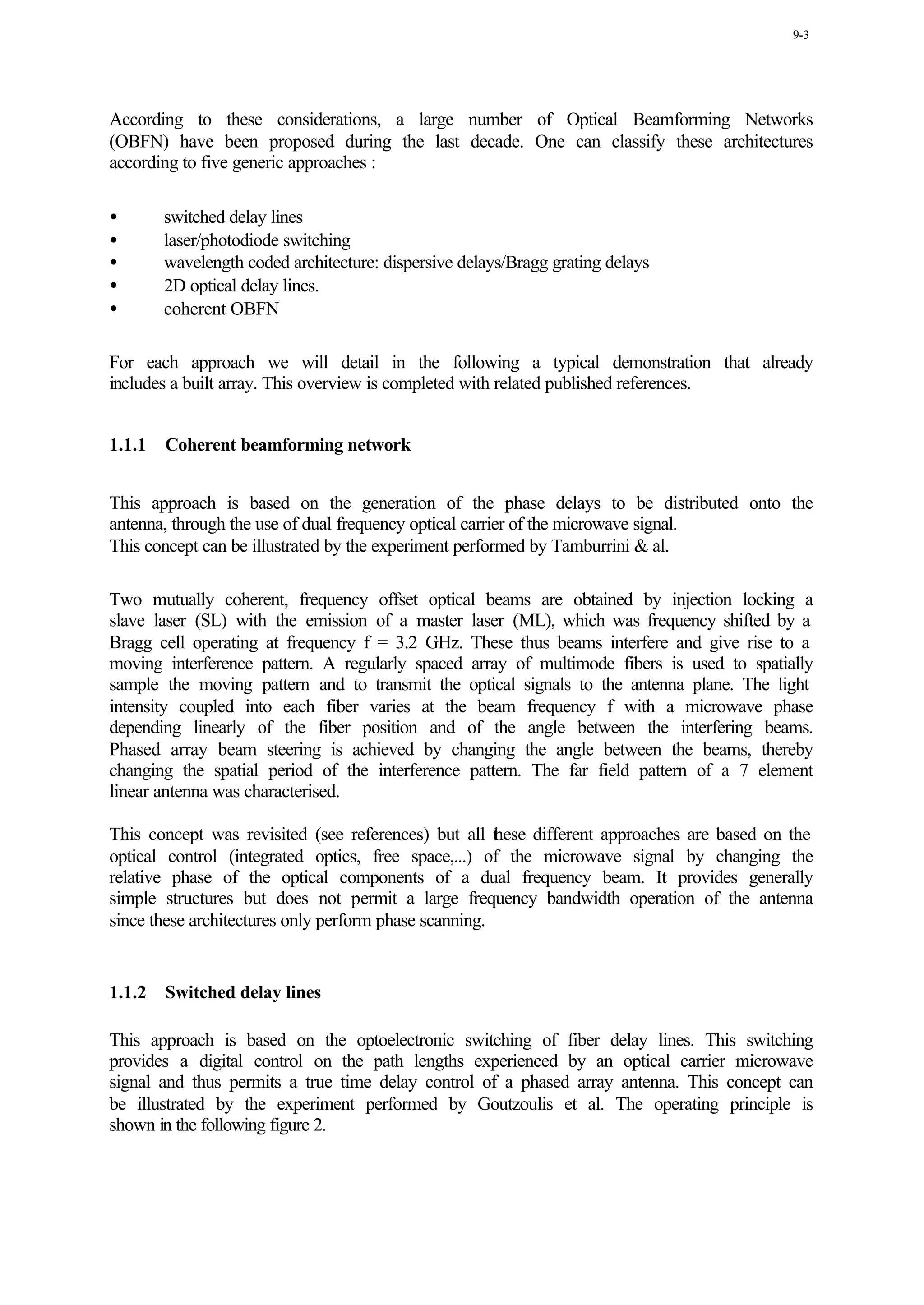
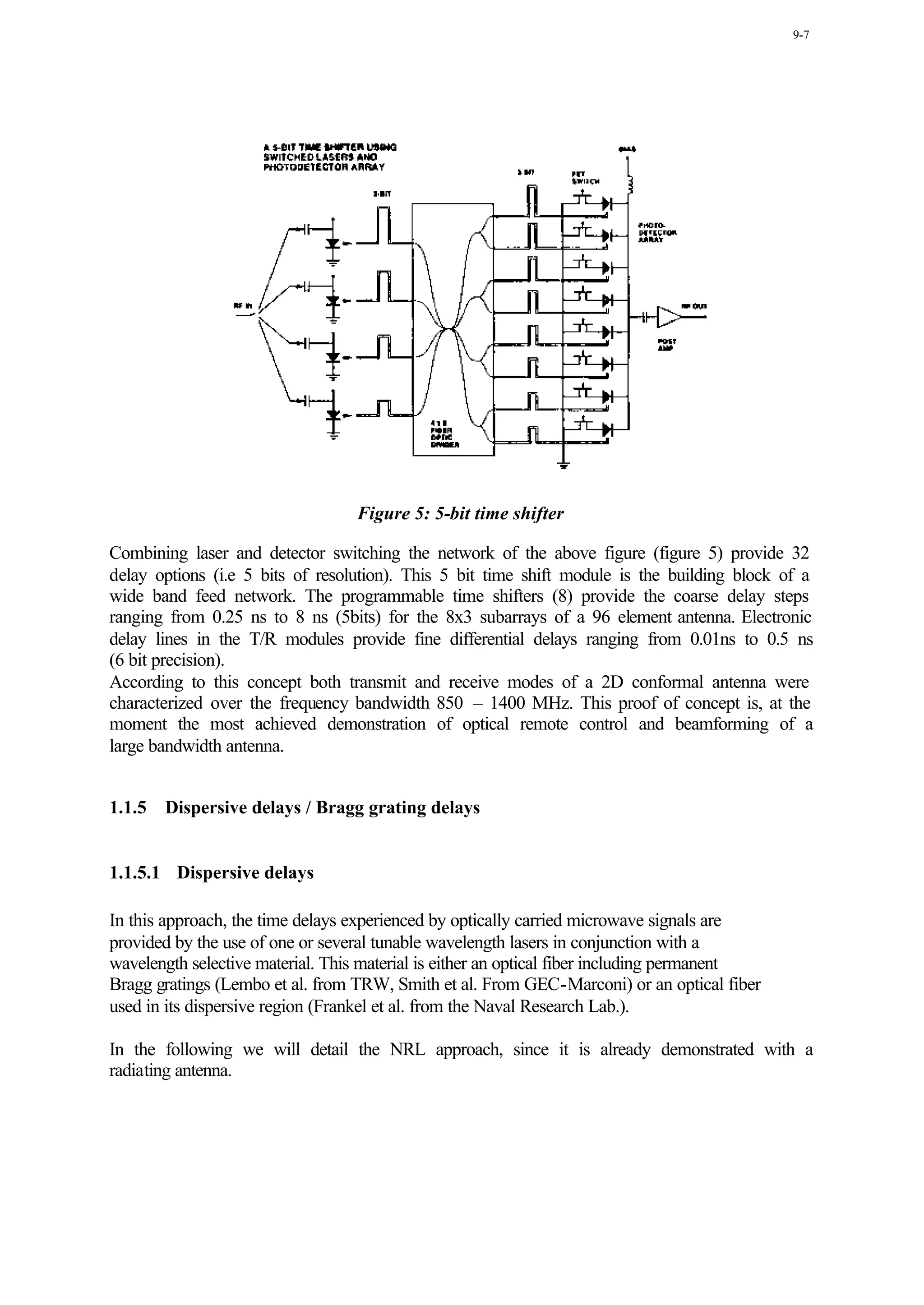
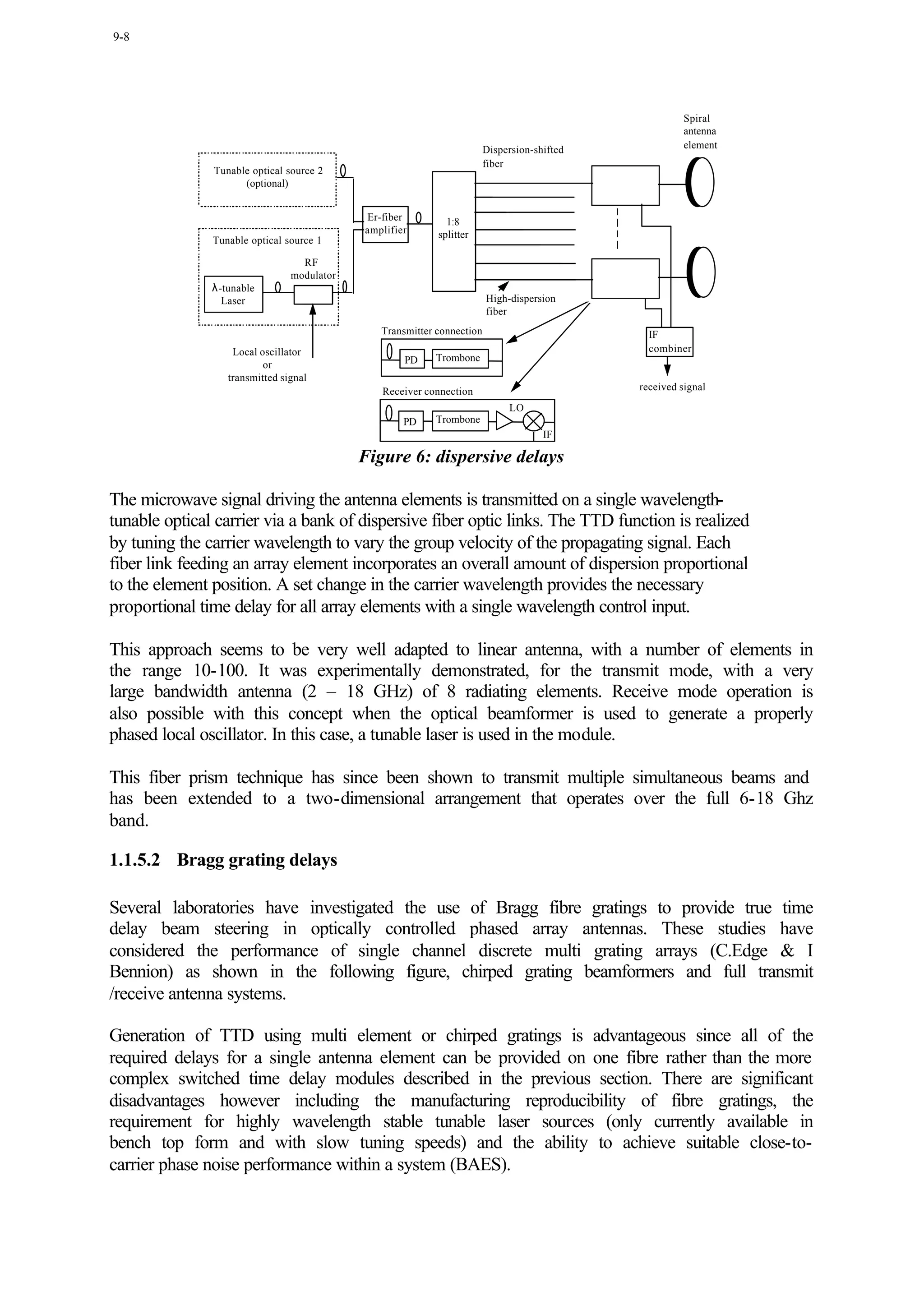
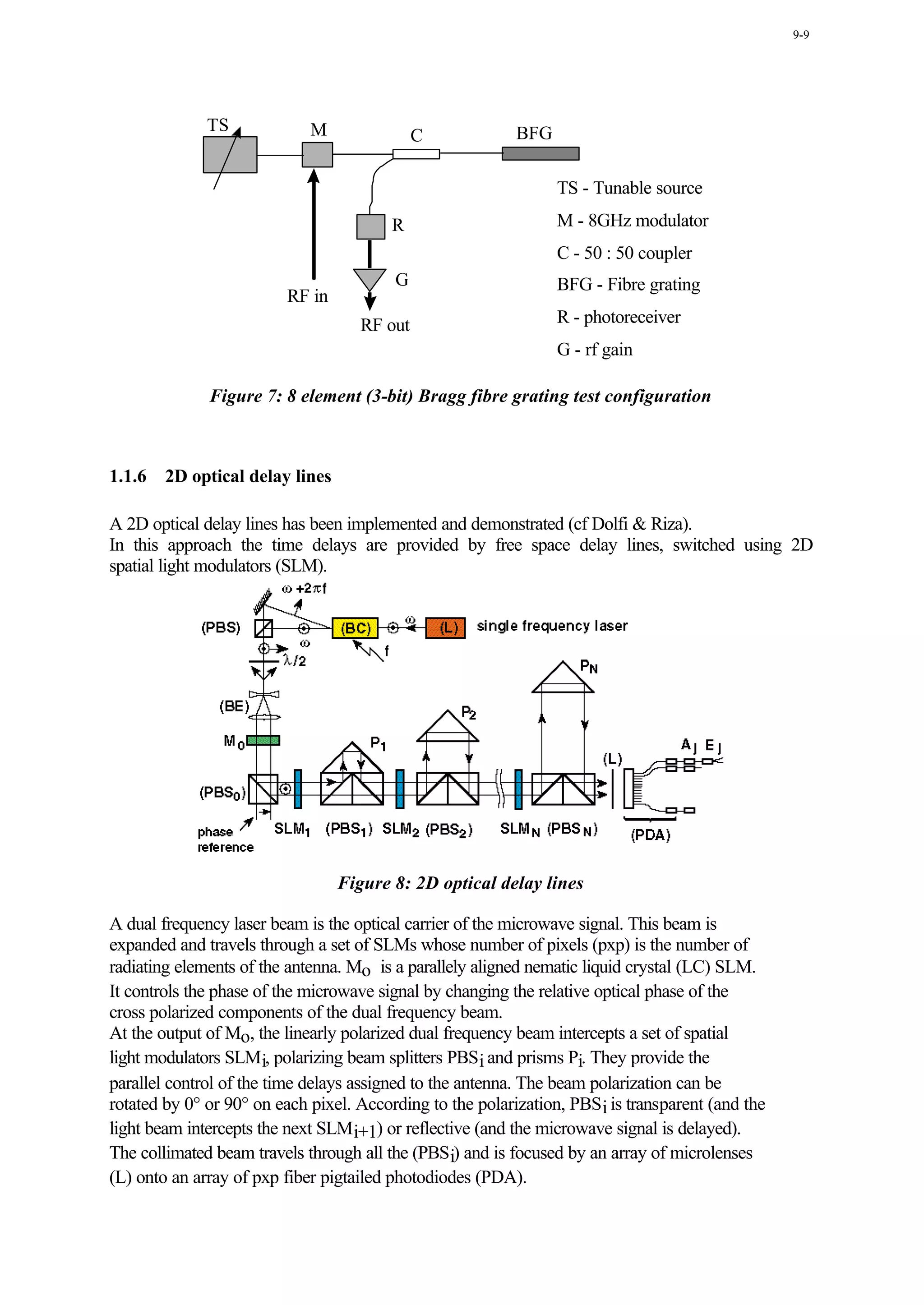
![9-10
For a given photodiode, the phase of the microwave beating signal is determined by the
applied voltage on the corresponding pixel of Mo and by the choice of the PBS i on which the
reflections occur. Since the positions of prisms Pi provide delay values according to a
geometric progression (t, 2t, 4t..), the beating signal can be delayed from 0 to (2N-1)t with
step t.
Experimental demonstration of an optically controlled phased array antenna, operating
between 2.5 and 3.5 GHz. The 2D architecture is implemented with 6 SLMs of 4 x 4 pixels. It
provides 32 delay values (5 bits), an analog control of the phase [0,2p] and permits the control
of a 16 element phased array antenna. Furthermore, when far field patterns at different
frequencies are superposed for a given scan direction , one can notice the absence of any
beam squint.
1.2 Optical Beamforming Receive Mode – Thomson-CSF 2D Approach
We propose and experimentally demonstrate two optical architectures performing processing
of the receive mode of a p×p element phased array antenna. They are based on free space
propagation and switching of channelized optical carriers of microwave signals. The first
architecture assumes a direct transposition of the received signals in the optical domain. The
second one is based on the optical generation and distribution of a microwave local oscillator
matched in frequency and direction. Preliminary experimental results at microwave
frequencies of about 3 GHz are presented.
The review presents an original architecture dedicated to the processing of the receive mode,
using a similar concept as the one demonstrated in for emission. In the Direct Architecture,
the received microwave signals are optically carried and travel back through the same time
delay network as the one used for the transmit mode. In the Matched Local Oscillator
Architecture (MLOA), a channelized microwave local oscillator, time delayed and optically
carried, is mixed, at the antenna level, to the received signals. It provides an heterodyne
filtering, matched in frequency and direction, to the received signal. Such an approach was
recently considered with quite different implementations. We propose here a third
implementation, fully programmable and based on the optical generation of simultaneous
complementary delays for both the transmit signal and the Local Oscillator (LO).
When now using this architecture in the receive mode, the microwave signal reflected by the
target travels back to the antenna, and is detected by an array of p×p microwave receivers.
The signals issued from each receiver are used to feed an array of modulated lasers (direct or
external modulation). For a radar detection in the same direction as for emission, the received
signals, optically carried, have to travel through the same time-delay network as the one used
for the emission mode. It permits in-phase addition over a large frequency bandwidth of all
×p
the microwave signals received by the antenna. An array of p photodiodes then extracts the
microwave information from the optical carriers for processing.
This detection mode leads to some important problems. Indeed, robustness to jamming
requires opto-electronic elements able to handle high power microwave signals. In the same
time, they must be able to detect very low level signals, corresponding to the target signatures
in limit of range. The ratio jammer signal to lower signal requires linearity of opto-links in the
range 100 – 120 dB. This corresponds to spurious free dynamic range (SFDR) in the range 70
– 80 dB/MHz2/3 . Such performances are still difficult to attain over large bandwidth with](https://image.slidesharecdn.com/en-028-all-120926115440-phpapp01/75/En-028-all-162-2048.jpg)
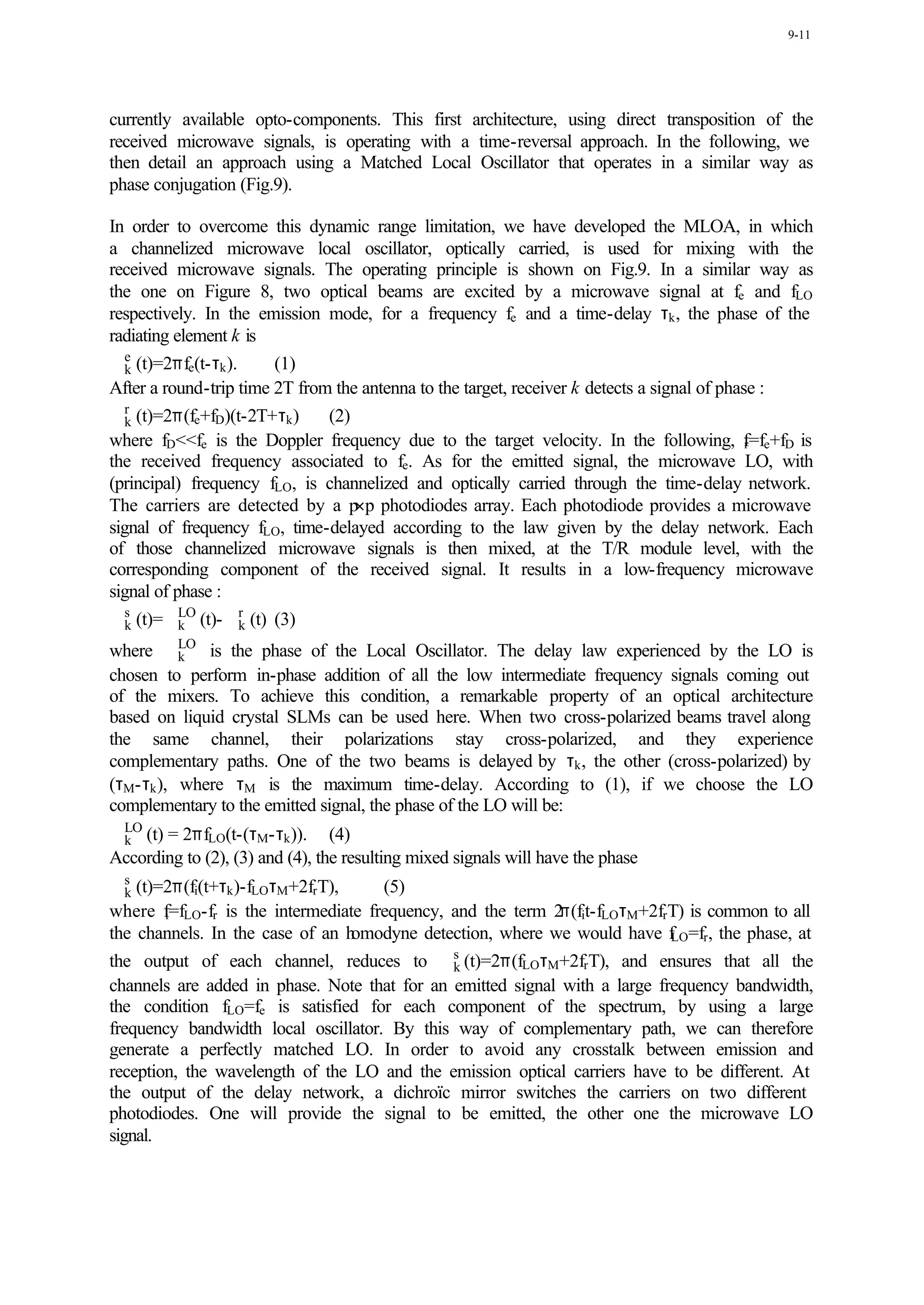
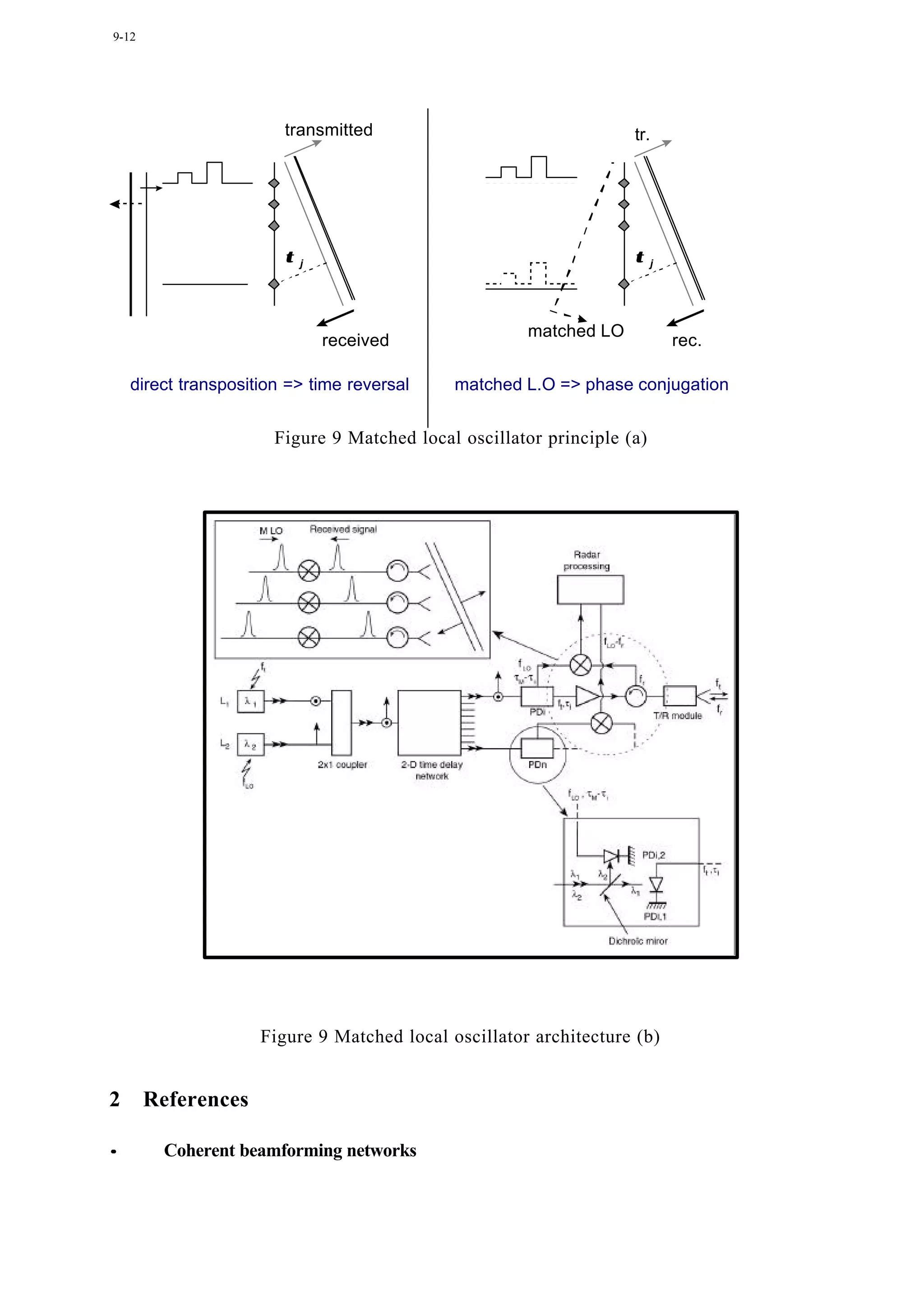
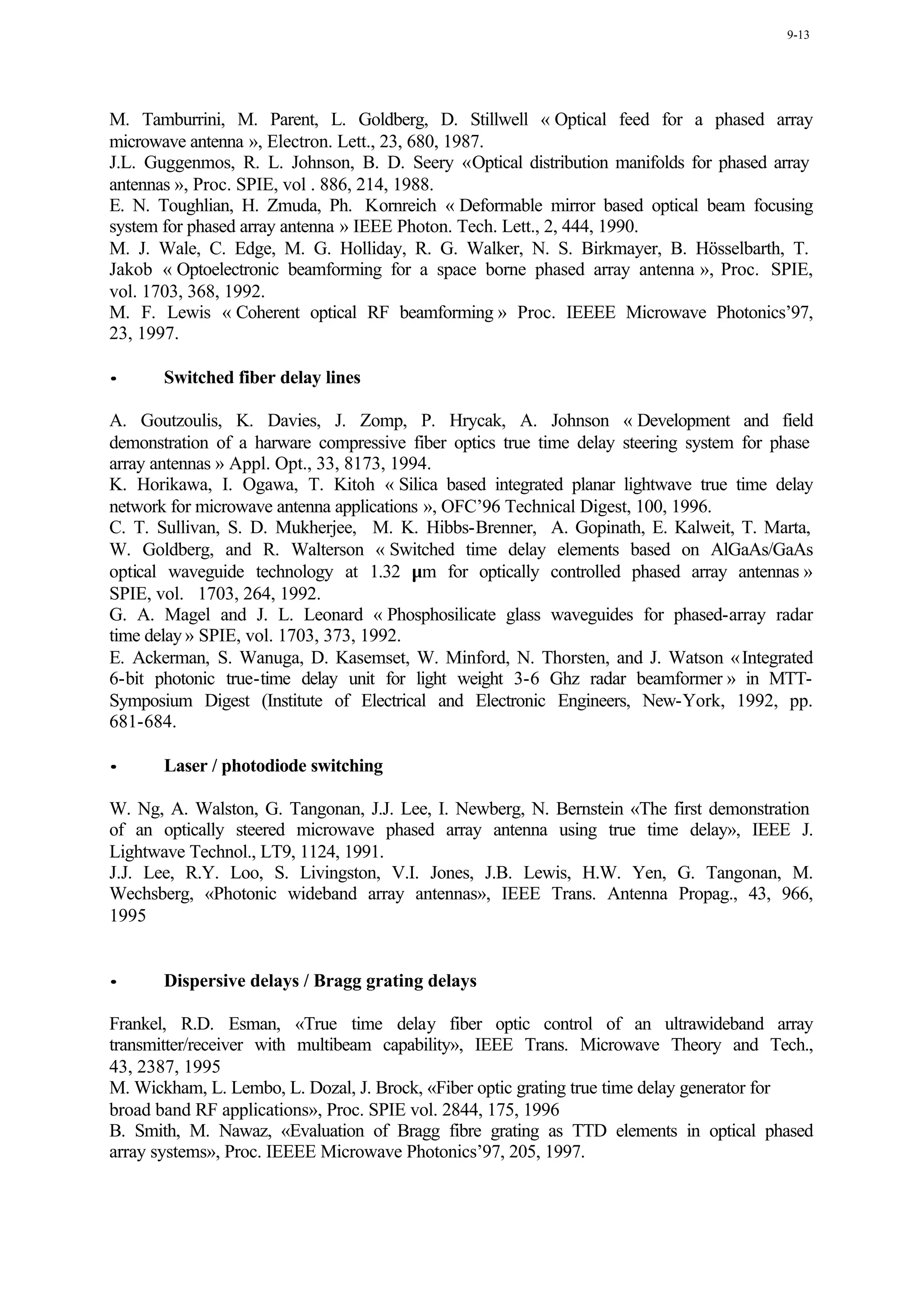


![Coded Agents – with UiPath SDK + LangGraph [Virtual Hands-on Workshop]](https://cdn.slidesharecdn.com/ss_thumbnails/codedagentsdeck-251215155422-5497c599-thumbnail.jpg?width=640&height=640&fit=bounds)


![Vibe Coding vs. Spec-Driven Development [Free Meetup]](https://cdn.slidesharecdn.com/ss_thumbnails/vibecodingvsspecdrivendevelopment-251209105622-43f455e7-thumbnail.jpg?width=640&height=640&fit=bounds)