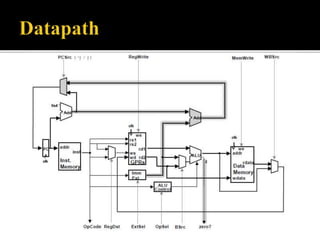
The DLX is a RISC processor architecture developed by John L. Hennessy and David A. Patterson, serving as a simplified version of the MIPS CPU. It features 32 general-purpose registers, a 32-bit register width, and utilizes three instruction types: R-type, I-type, and J-type. The document outlines specific instructions and their binary opcodes for operations such as addition, subtraction, and memory access.

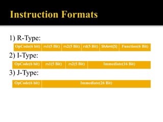
![IR[31:26] IR[5:0] Instruction Operation
000000 0x00 101100 0x2c sls RD = (RS1 < RS2 ? 1 : 0)
000000 0x00 100010 0x22 sub RD = RS1 - RS2
000000 0x00 100000 0x20 add RD = RS1 + RS2
000000 0x00 100100 0x24 and RD = RS1 AND RS2
000000 0x00 100101 0x25 or RD = RS1 OR RS2
000100 0x04 ------- ------- beqz PC = PC + 4 + (RS1 = 0 ? SignExt(imm) : 0)
100011 0x23 ------- ------- lw RD = mem
101011 0x2b ------- ------- sw mem = RD
001000 0x08 addi RD = RS1 + SignExt(imm)](https://image.slidesharecdn.com/dlxdatapath-fatemeafshar-mohsenzandi-171218204606/85/DLX-Architecture-4-320.jpg)