BVD-Lecture-3
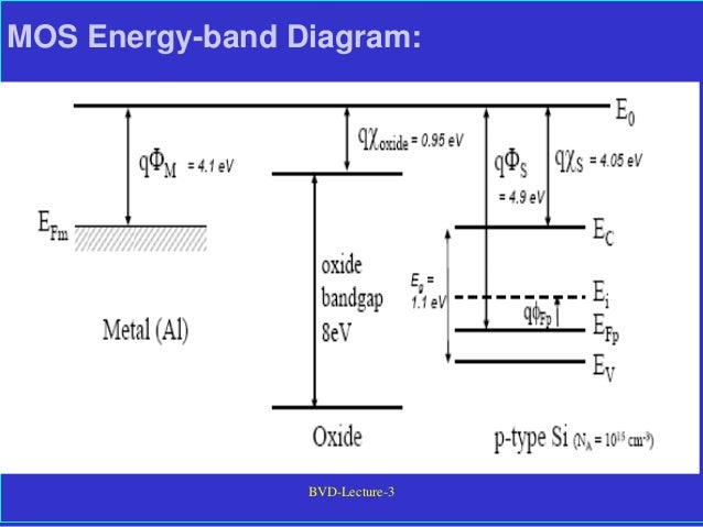
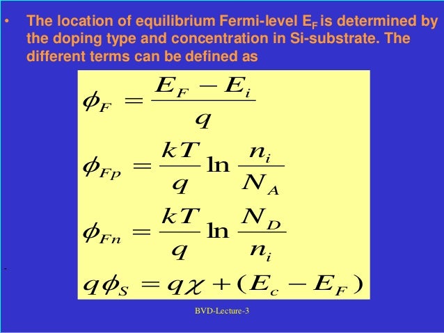
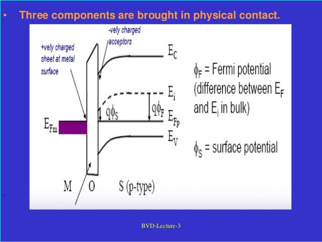
• The locationof equilibrium Fermi-level EF is determined by
the doping type and concentration in Si-substrate. The
different terms can be defined as
)
(
ln
ln
F
c
S
i
D
Fn
A
i
Fp
i
F
F
E
E
q
q
n
N
q
kT
N
n
q
kT
q
E
E
BVD-Lecture-3
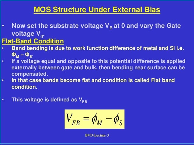
MOS Structure UnderExternal Bias
• Now set the substrate voltage VB at 0 and vary the Gate
voltage Vg.
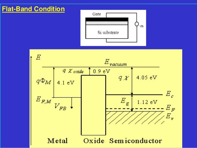
Flat-Band Condition
• Band bending is due to work function difference of metal and Si i.e.
ΦM – ΦS.
• If a voltage equal and opposite to this potential difference is applied
externally between gate and bulk, then bending near surface can be
compensated.
• In that case bands become flat and condition is called Flat band
condition.
• This voltage is defined as VFB
S
M
FB
V
BVD-Lecture-3
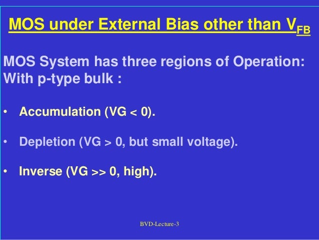
MOS under ExternalBias other than VFB
MOS System has three regions of Operation:
With p-type bulk :
• Accumulation (VG < 0).
• Depletion (VG > 0, but small voltage).
• Inverse (VG >> 0, high).
9.
BVD-Lecture-3
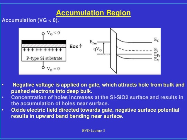
Accumulation Region
Accumulation (VG< 0).
• Negative voltage is applied on gate, which attracts hole from bulk and
pushed electrons into deep bulk.
• Concentration of holes increases at the Si-SiO2 surface and results in
the accumulation of holes near surface.
• Oxide electric field directed towards gate, negative surface potential
results in upward band bending near surface.
10.
BVD-Lecture-3
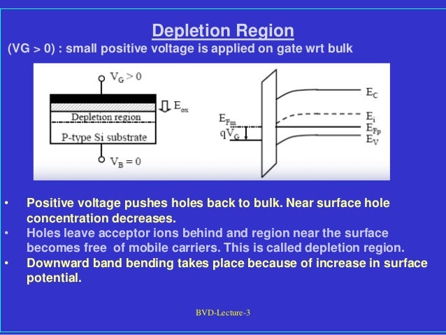
Depletion Region
(VG >0) : small positive voltage is applied on gate wrt bulk
• Positive voltage pushes holes back to bulk. Near surface hole
concentration decreases.
• Holes leave acceptor ions behind and region near the surface
becomes free of mobile carriers. This is called depletion region.
• Downward band bending takes place because of increase in surface
potential.
11.
BVD-Lecture-3
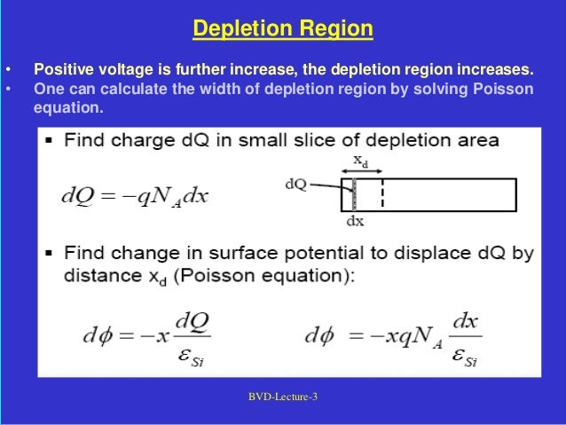
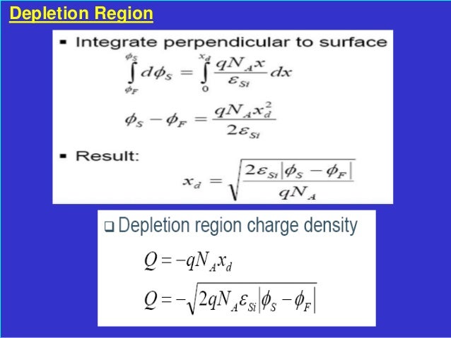
Depletion Region
• Positivevoltage is further increase, the depletion region increases.
• One can calculate the width of depletion region by solving Poisson
equation.
BVD-Lecture-3
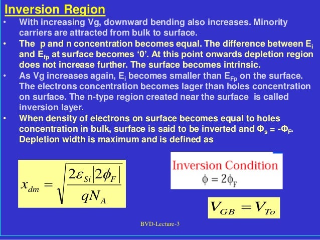
Inversion Region
• Withincreasing Vg, downward bending also increases. Minority
carriers are attracted from bulk to surface.
• The p and n concentration becomes equal. The difference between Ei
and Efp at surface becomes ‘0’. At this point onwards depletion region
does not increase further. The surface becomes intrinsic.
• As Vg increases again, Ei becomes smaller than EFp on the surface.
The electrons concentration becomes lager than holes concentration
on surface. The n-type region created near the surface is called
inversion layer.
• When density of electrons on surface becomes equal to holes
concentration in bulk, surface is said to be inverted and Φs = -ΦF.
Depletion width is maximum and is defined as
A
F
Si
dm
qN
x
2
2
To
GB V
V
14.
BVD-Lecture-3
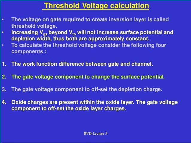
Threshold Voltage calculation
•The voltage on gate required to create inversion layer is called
threshold voltage.
• Increasing Vgs beyond Vto will not increase surface potential and
depletion width, thus both are approximately constant.
• To calculate the threshold voltage consider the following four
components :
1. The work function difference between gate and channel.
2. The gate voltage component to change the surface potential.
3. The gate voltage component to off-set the depletion charge.
4. Oxide charges are present within the oxide layer. The gate voltage
component to off-set the oxide layer charges.
15.
BVD-Lecture-3
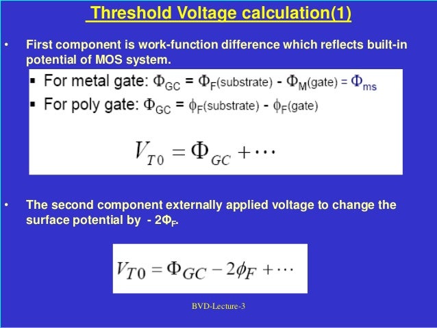
Threshold Voltage calculation(1)
•First component is work-function difference which reflects built-in
potential of MOS system.
• The second component externally applied voltage to change the
surface potential by - 2ΦF.
16.
BVD-Lecture-3
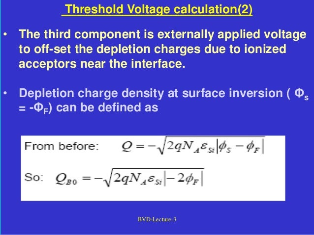
Threshold Voltage calculation(2)
•The third component is externally applied voltage
to off-set the depletion charges due to ionized
acceptors near the interface.
• Depletion charge density at surface inversion ( Φs
= -ΦF) can be defined as
17.
BVD-Lecture-3
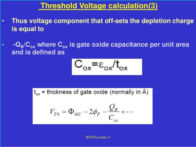
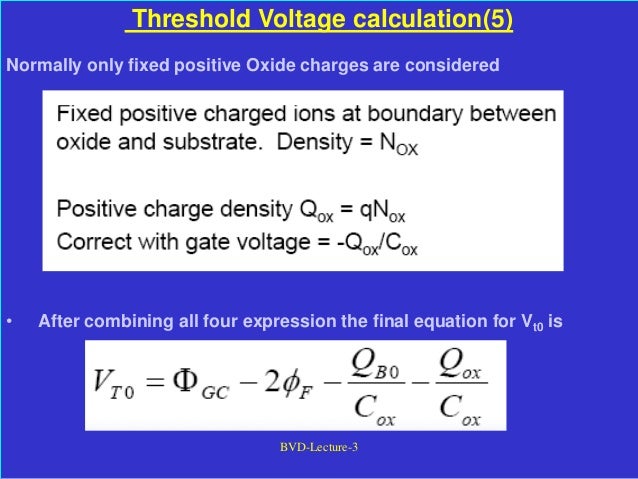
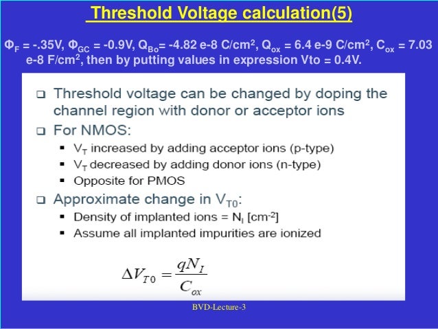
Threshold Voltage calculation(3)
•Thus voltage component that off-sets the depletion charge
is equal to
• -QB/Cox where Cox is gate oxide capacitance per unit area
and is defined as
18.
BVD-Lecture-3
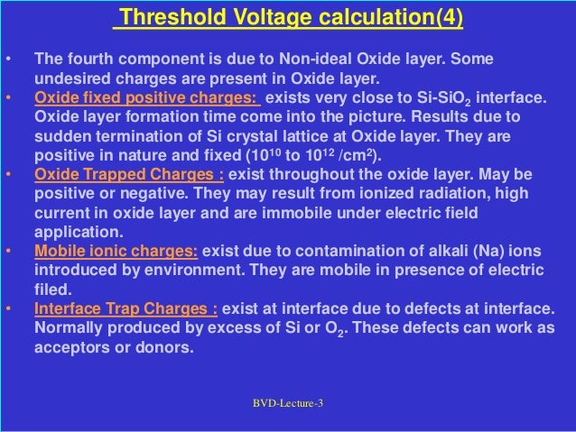
Threshold Voltage calculation(4)
•The fourth component is due to Non-ideal Oxide layer. Some
undesired charges are present in Oxide layer.
• Oxide fixed positive charges: exists very close to Si-SiO2 interface.
Oxide layer formation time come into the picture. Results due to
sudden termination of Si crystal lattice at Oxide layer. They are
positive in nature and fixed (1010 to 1012 /cm2).
• Oxide Trapped Charges : exist throughout the oxide layer. May be
positive or negative. They may result from ionized radiation, high
current in oxide layer and are immobile under electric field
application.
• Mobile ionic charges: exist due to contamination of alkali (Na) ions
introduced by environment. They are mobile in presence of electric
filed.
• Interface Trap Charges : exist at interface due to defects at interface.
Normally produced by excess of Si or O2. These defects can work as
acceptors or donors.