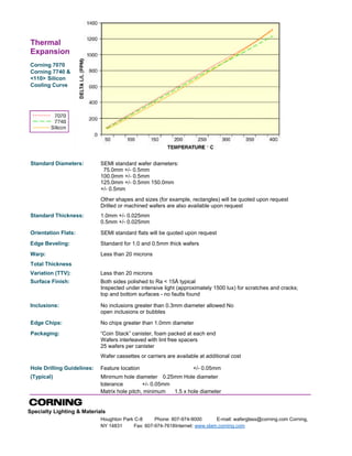
Glass Silicon Constraint Substrates
Corning supplies a variety of polished and machined glass wafers for use in the fast-growing MST/MEMS (Micro
Systems Technology/Micro-Electrical-Mechanical Systems) technologies.
The substrates are produced using the industry standard Pyrex®
(Corning code 7740) and other silicon thermal
expansion matching glasses, such as Corning code 7070; coupled with innovative manufacturing techniques,
world class measurement, and global sales and technical support.
Materials: Pyrex® 7740 Borosilicate Glass
7070 Lithia Potash Borosilicate
Glass Properties: 7740 7070
Mechanical Density (g•cm-3) 2.23 2.13
Young Modulus (G Pa) 62.75 51.00
Poisson Ratio 0.20 0.22
CTE, 0-300°C (x10-6•°C-1) 3.25 3.20
Viscosity Working Point (°C) 104 Poise 1252 1068
Softening Point (°C) 107.6 Poise 821 n/a
Annealing Point (°C) 1013 Poise 560 496
Strain Point (°C) 1014 Poise 510 456
Electrical Log volume resistivity (Ωcm): 250°C, 350°C 6.1, 4.6 11.2, 9.1
Dielectric Constant, 20°C, 1MHz 4.6 4.1
Loss Tangent, 20°C, 1 MHz (%) 0.5 0.06
Standard Diameters: SEMI standard wafer diameters:
75.0mm +/- 0.5mm
100.0mm +/- 0.5mm
125.0mm +/- 0.5mm 150.0mm
+/- 0.5mm
Other shapes and sizes (for example, rectangles) will be quoted upon request
Drilled or machined wafers are also available upon request
Standard Thickness: 1.0mm +/- 0.025mm
0.5mm +/- 0.025mm
Orientation Flats: SEMI standard flats will be quoted upon request
Edge Beveling: Standard for 1.0 and 0.5mm thick wafers
Warp:
Total Thickness
Less than 20 microns
Variation (TTV): Less than 20 microns
Surface Finish: Both sides polished to Ra < 15Å typical
Inspected under intensive light (approximately 1500 lux) for scratches and cracks;
top and bottom surfaces - no faults found
Inclusions: No inclusions greater than 0.3mm diameter allowed No
open inclusions or bubbles
Edge Chips: No chips greater than 1.0mm diameter
Packaging: “Coin Stack” canister, foam packed at each end
Wafers interleaved with lint free spacers
25 wafers per canister
Wafer cassettes or carriers are available at additional cost
Hole Drilling Guidelines: Feature location +/- 0.05mm
(Typical) Minimum hole diameter 0.25mm Hole diameter
tolerance +/- 0.05mm
Matrix hole pitch, minimum 1.5 x hole diameter
Specialty Lighting & Materials
Houghton Park C-8 Phone: 607-974-9000 E-mail: waferglass@corning.com Corning,
NY 14831 Fax: 607-974-7618Internet: www.slam.corning.com
Thermal
Expansion
Corning 7070
Corning 7740 &
<110> Silicon
Cooling Curve
To Know more info visit this link : http://www.valleydesign.com/pyrex.htm
1M 20.82 6/99 Goff

Corning Pyrex 7740 & Properties

  • 1.
    Glass Silicon ConstraintSubstrates Corning supplies a variety of polished and machined glass wafers for use in the fast-growing MST/MEMS (Micro Systems Technology/Micro-Electrical-Mechanical Systems) technologies. The substrates are produced using the industry standard Pyrex® (Corning code 7740) and other silicon thermal expansion matching glasses, such as Corning code 7070; coupled with innovative manufacturing techniques, world class measurement, and global sales and technical support. Materials: Pyrex® 7740 Borosilicate Glass 7070 Lithia Potash Borosilicate Glass Properties: 7740 7070 Mechanical Density (g•cm-3) 2.23 2.13 Young Modulus (G Pa) 62.75 51.00 Poisson Ratio 0.20 0.22 CTE, 0-300°C (x10-6•°C-1) 3.25 3.20 Viscosity Working Point (°C) 104 Poise 1252 1068 Softening Point (°C) 107.6 Poise 821 n/a Annealing Point (°C) 1013 Poise 560 496 Strain Point (°C) 1014 Poise 510 456 Electrical Log volume resistivity (Ωcm): 250°C, 350°C 6.1, 4.6 11.2, 9.1 Dielectric Constant, 20°C, 1MHz 4.6 4.1 Loss Tangent, 20°C, 1 MHz (%) 0.5 0.06
  • 2.
    Standard Diameters: SEMIstandard wafer diameters: 75.0mm +/- 0.5mm 100.0mm +/- 0.5mm 125.0mm +/- 0.5mm 150.0mm +/- 0.5mm Other shapes and sizes (for example, rectangles) will be quoted upon request Drilled or machined wafers are also available upon request Standard Thickness: 1.0mm +/- 0.025mm 0.5mm +/- 0.025mm Orientation Flats: SEMI standard flats will be quoted upon request Edge Beveling: Standard for 1.0 and 0.5mm thick wafers Warp: Total Thickness Less than 20 microns Variation (TTV): Less than 20 microns Surface Finish: Both sides polished to Ra < 15Å typical Inspected under intensive light (approximately 1500 lux) for scratches and cracks; top and bottom surfaces - no faults found Inclusions: No inclusions greater than 0.3mm diameter allowed No open inclusions or bubbles Edge Chips: No chips greater than 1.0mm diameter Packaging: “Coin Stack” canister, foam packed at each end Wafers interleaved with lint free spacers 25 wafers per canister Wafer cassettes or carriers are available at additional cost Hole Drilling Guidelines: Feature location +/- 0.05mm (Typical) Minimum hole diameter 0.25mm Hole diameter tolerance +/- 0.05mm Matrix hole pitch, minimum 1.5 x hole diameter Specialty Lighting & Materials Houghton Park C-8 Phone: 607-974-9000 E-mail: waferglass@corning.com Corning, NY 14831 Fax: 607-974-7618Internet: www.slam.corning.com Thermal Expansion Corning 7070 Corning 7740 & <110> Silicon Cooling Curve
  • 3.
    To Know moreinfo visit this link : http://www.valleydesign.com/pyrex.htm 1M 20.82 6/99 Goff