Downloaded 463 times


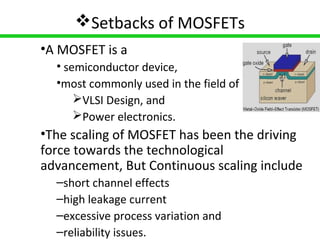
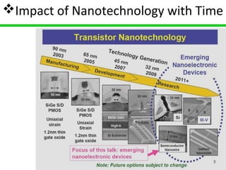
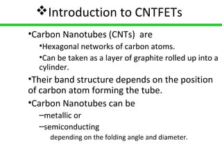
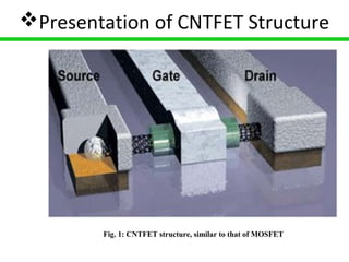
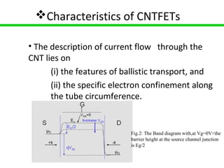


Carbon nanotube field-effect transistors (CNTFETs) have advantages over traditional MOSFETs by avoiding issues like short channel effects and high leakage currents that arise from continuous MOSFET scaling. CNTFETs use carbon nanotubes that can be metallic or semiconducting depending on their structure. They have a similar structure to MOSFETs but current flow depends on ballistic transport and electron confinement in the CNT. CNTFETs also have lower quantum capacitance than MOSFETs, resulting in lower propagation delay. Neural networks are well-suited for modeling CNTFETs with their simple, continuous equations that can account for channel length variations. However, precisely controlling CNT