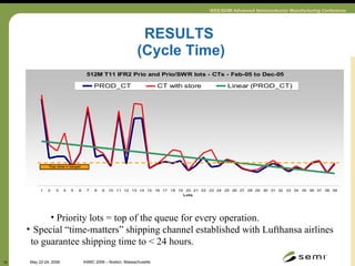
The document discusses methods for improving the cycle time and yield learning between a DRAM wafer fabrication facility and a remote packaging and test site located some distance away. It describes implementing priority dispatching, special shipping channels, and real-time data transfer to reduce the cycle time from 2 days to less than 24 hours. Quality control gates and lot attributes were also added to the remote test site's systems to help with risk containment and allow non-standard processing for experimental evaluations, resulting in a 30% higher volume of experimental lots being processed and twice the theoretical learning rate.