Investigation of Power Quality Improvement in Super Lift Luo Converter
SAIKAT-VECC final
1. 1 | P a g e
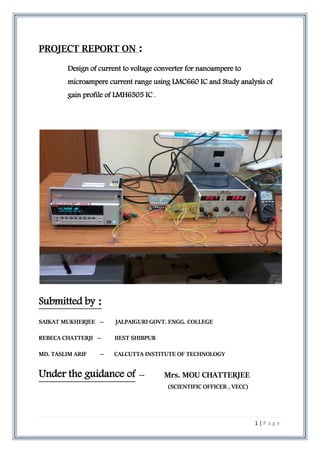
PROJECT REPORT ON :
Design of current to voltage converter for nanoampere to
microampere current range using LMC660 IC and Study analysis of
gain profile of LMH6505 IC .
Submitted by :
SAIKAT MUKHERJEE -- JALPAIGURI GOVT. ENGG. COLLEGE
REBECA CHATTERJI -- IIEST SHIBPUR
MD. TASLIM ARIF -- CALCUTTA INSTITUTE OF TECHNOLOGY
Under the guidance of -- Mrs. MOU CHATTERJEE
(SCIENTIFIC OFFICER , VECC)
2. 2 | P a g e
ACKNOWLEDGEMENT
The project entitled “ Design of current to voltage converter for nanoampere to
microampere current range using the LMC660 IC and study analysis of gain profile of
LMH6505 IC ” was carried out by us at VARIABLE ENERGY CYCLOTRON CENTER ,
DEPARTMENT OF ATOMIC ENERGY , SALTLAKE , KOLKATA -700064 .
We would like to offer our profound gratitude and sincere regards to our project guide
Mrs. Mou Chatterjee for her immense support and constant guidance .
We are also grateful to Mr. Dhananjoy Koley for his needful suggestions and untiring help
throughout our period of work at VECC.
We would like to extend my gratitude to Mr. P.Y. Nabhiraj for providing us with the
opportunity to carry out our project work at VECC.
We are immensely proud to be associated with the ECRISF section of VECC , which happens
to be one of the most prestigious and pioneering research institutes of India.
We are extremely thankful to all the members of ECRISF section for providing various
facilities to us in order to carry out our project work.
3. 3 | P a g e
OBJECTIVE
The project is mainly comprised of two parts :
(a) Design of a current to voltage converter for the conversion of currents in the range of 1
nA to 1µA into equivalent voltage with a conversion rate of 1µA/V.
(b) Study Analysis of the gain profile of LMH6505 IC .
The current to voltage converter has been designed using National Instrument’s
Quad CMOS Op-Amp IC namely LMC660CN. This converter was used for the
conversion of currents in the range of 1 nA to 1µA into equivalent voltages. The I-V
converter has a fixed feedback resistance of 1 MΩ with a conversion rate of 1µA/V .
The circuit for the current to voltage converter was designed using PROTEUS-ISIS
software. The PCB layout for the I-V converter was designed using PROTEUS-ARES
software.
4. 4 | P a g e
Also , the analysis of gain profile of Texas Instrument’s LMH6505 IC was done
for changing resistive component values . The maximum value of the gain of
the IC was set by fixing the values of the component resistances . Besides the
maximum input voltage limits and Bandwidth considerations were also
analyzed during the course of this project. The input voltage to the LMH6505
IC was set to a value of 0.5 Volts and the various gain values were computed
for changing values of the gain control voltage. Finally the plots for gain vs
control voltage were plotted and the results analyzed.
5. 5 | P a g e
(A) DESIGN OF A CURRENT TO VOLTAGE
CONVERTER FOR CURRENTS IN THE
RANGE OF nA- µA WITH A CONVERSION
RATE OF 1µA/V
6. 6 | P a g e
OBJECTIVE
In the first part of our project we were required to design a current to voltage converter
which could convert currents in the range of 1 nA to 1µA into equivalent voltages. The
Quad operational amplifier IC LMC660CN from National Instruments having ultra low bias
current of 2 fA has been chosen as the current to voltage ( I to V) converter.
The full range of measurement from 1 nA to 1 µA has been covered with the help of a
feedback resistance of 1 MΩ ±1% .The conversion rate of the current to voltage converter
has been measured as 1µA/V.
7. 7 | P a g e
COMPONENTS USED FOR THE DESIGN OF
CURRENT TO VOLTAGE CONVERTER
CMOS Quad Operational Amplifier IC LMHC660CN
Keithley 6220 Precision Current Source
1 MΩ Resistances
15 pF Capacitors
Mean Well RT - 50C power supply
8. 8 | P a g e
470 Ω resistances
1N4740A zener diodes
Digital multimeter
5 Pin connector
2 Pin connector
9. 9 | P a g e
The CMOS Quad Op-Amp IC LMC660CN
The LMC660CN is a Quad operational amplifier IC. It is based on CMOS technology and
has been built with National Instrument’s advanced Double PolySilicon-Gate CMOS
process. It operates from +5V to +15.5V and features rail-to-rail output swing in addition to
an input common-mode range that includes ground.
Performance limitations that have plagued CMOS amplifiers in the past are not a problem
with this design. Input VOS, drift, and broadband noise as well as voltage gain into realistic
loads (2 kΩ and 600Ω) are all equal to or better than widely accepted bipolar equivalents.
The salient features of this IC include :-
Rail to Rail Output swing : +5 V to +15.5 V
Specified for loads : 2KΩ and 600Ω .
High Voltage Gain : 126 dB
Low Input Offset Voltage : 3mV
Ultra low input bias current : 2 fA
Low distortion : 0.01 % at 10 kHZ
Slew Rate : 1.1 V/µs
Low offset voltage drift : 1.3 µV/°C
10. 10 | P a g e
The pin diagram of the IC LMC660CN is as shown below :
The various applications of the CMOS Quad op-amp IC LMC660CN are as follows :
1. High impedance buffer or pre-amplifier .
2. Precision current to voltage converter .
3. Long term integrator .
4. Sample and Hold Circuit .
5. Peak detector .
6. Medical Instrumentation .
7. Industrial Controls .
8. Automotive sensors .
11. 11 | P a g e
BASIC THEORETICAL DESIGN OF THE
CURRENT TO VOLTAGE CONVERTER
During the starting phase of analysis the basic theoretical design and circuit diagram of a
current to voltage converter were designed . The current in the range of 1 nA to 1 µA is fed
as input to the first op-amp which produces an equivalent inverted voltage as output . This
output of the first op-amp is fed as input to the second op-amp which produces the same
voltage as output but with a zero degree phase shift . Hence an equivalent voltage is
obtained for the input current in the range of nanoamperes to microamperes . The
equivalent voltage obtained is in the range of 1mV – 1V . Negative feedback technique is
used with the help of 1 MΩ resistors which stabilize the gain and provide a conversion rate
of 1 µA/V .
12. 12 | P a g e
PRACTICAL IMPLEMENTATION OF
THEORETICAL DESIGN OF CURRENT TO
VOLTAGE CONVERTER
During practical implementation of the current to voltage converter as in the theoretical
design the CMOS Quad op-amp IC- LMC660CN was used. The Power supplies used for pin
4 and pin 11 of LMC660CN were +10V and -10 V respectively.
The generation of +10 V and -10 V supplies were done with the help of 1N4740A zener
diodes , 470 Ω resistors and ±15V power supply. The 1N4740A zeners have voltage rating
of 10 volts and maximum power rating of 1 Watt . The ouputs of the two 1N4740A zeners
were fed to the pins 4 and 11 of LMHC660CN respectively .
13. 13 | P a g e
CIRCUIT DIAGRAM OF GENERATION OF ±10V
POWER SUPPLIES USING 1N4740A
The circuit diagram for generation of +10 V using 1N4740A zener is shown below :
The circuit diagram for generation of -10 V using 1N4740A zener is shown below :
14. 14 | P a g e
DESIGN OF CURRENT TO VOLTAGE CONVERTER
ON BREADBOARD AND MEASURING
CORRESPONDING OUTPUT VALUES
During the preliminary stages , the current to voltage converter was designed on a
breadboard and the readings noted .
OBSERVATION TABLE FOR I-V CONVERTER DESIGNED
ON BREADBOARD
CURRENT (µA) VOLTAGE ( volts )
1 µA 0.97 V
2 µA 1.98 V
3 µA 2.98 V
4 µA 3.98 V
5 µA 4.98 V
6 µA 5.98 V
7 µA 6.98 V
8 µA 7.98 V
9 µA 8.98 V
10 µA 9.70 V
CURRENT (nA) VOLTAGE (mV)
1 nA 0.6 mV
2 nA 1.6 mV
3 nA 2.6 mV
4 nA 3.6 mV
5 nA 4.6 mV
6 nA 5.6 mV
7 nA 6.6 mV
8 nA 7.6 mV
9 nA 8.6 mV
10 nA 9.6 mV
15. 15 | P a g e
PCB DESIGN OF I-V CONVERTER
COMPONENTS REQUIRED :
Copper Clad Board
Soldering iron
Solder wire
Electric iron
Anhydrous Ferric Chloride
16. 16 | P a g e
PCB
A printed circuit board (PCB) mechanically supports and electrically connects electronic
components using conductive tracks, pads and other features etched from copper
sheets laminated onto a non-conductive substrate. PCBs can be single sided (one copper
layer), double sided (two copper layers) or multi-layer (outer and inner layers). Multi-layer
PCBs allow for much higher component density. Conductors on different layers are
connected with plated-through holes called vias. Advanced PCBs may contain components
– capacitors, resistors or active devices – embedded in the substrate.
Printed circuit boards are used in all but the simplest electronic products. Alternatives to
PCBs include wire wrap and point-to-point construction. PCBs require the additional
design effort to lay out the circuit, but manufacturing and assembly can be automated.
Manufacturing circuits with PCBs is cheaper and faster than with other wiring methods as
components are mounted and wired with one single part. Furthermore, operator wiring
errors are eliminated.
.
17. 17 | P a g e
STEPS IN PCB DESIGN OF I-V CONVERTER :
1 ) The design of circuit schematic on PROTEUS-ISIS software :
18. 18 | P a g e
2) Design of PCB layout on PROTEUS-ARES software :
19. 19 | P a g e
3) After the design of PCB layout on the PROTEUS – ARES software
The following steps were performed thereafter :-
A printout of the layout was taken on a piece of photopaper.
A copper clad board of dimensions 11.6 cm × 6.2 cm was taken. The board was first
rubbed with emery paper to remove any oxide coating from the board.
The photopaper was then placed on the copper board with its printed side pressed
against the board .
An electric iron was taken and it was used to press the photopaper against the
copper clad board. The electric iron was moved on the board until the photopaper
turned reddish brown in colour.
The electric iron was switched off and the copper board with the photopaper on it
was allowed to cool for sometime .
The photopaper automatically got separated from the copper clad board . Thus an
imprint of the whole circuit was created on the board .
20. 20 | P a g e
Finally a solution of anhydrous ferric chloride solution was prepared in a container
and the copper clad board with the imprint on it was placed in the solution . The
copper clad board was etched chemically and finally our PCB was ready for use.
Next holes were drilled in the required places on the printed circuit board using
advanced drilling machine .
The components were then soldered onto the PCB board using a 25 W soldering
iron. The soldering was done carefully to avoid short circuit between various paths
of the PCB .
Our final PCB is as shown below :
21. 21 | P a g e
DESIGN ISSUES
While designing the current to voltage converter , some critical issues were taken care of
such as compensating the input capacitance of the amplifier , proper component soldering
and PCB layout .
COMPENSATING INPUT CAPACITANCE :-
The high input resistance of the LMC660 op-amp allows the use of large feedback and
source resistances without losing gain accuracy due to loading . However such large valued
resistances make the circuit extremely sensitive to its layout.
Every amplifier has some capacitance between each input and AC ground and some
differential capacitance between the inputs. When resistive feedback network is used for an
amplifier , this input capacitance along with feedback resistors create a pole in the feedback
path .
For a general operational amplifier the frequency of this pole is given by:
𝒇𝒑 = (
𝟏
𝟐𝝅𝑪𝒔𝑹𝒑
)..................(1)
where Cs is the total capacitance at the inverting input including amplifier input and stray
capacitance , circuit board capacitance .
Rs is the parallel combination of RF and RIN , where RF is the feedback resistance and RIN is
the inverting resistance .
22. 22 | P a g e
For LMC660 , the RIN > 1 TΩ , RF is chosen to be 1 MΩ and generally CS is less than 10 pF .
Hence , from the above equation the frequency of the pole calculated is as follows :
𝒇𝒑 = [
𝟏
𝟐𝝅 × 𝟏𝟎 × 𝟏𝟎−𝟏𝟐 × ( 𝟏 𝑴Ω ‖ 𝟏 𝑻Ω)
]
A feedback capacitor is connected between the output and inverting input of the
operational amplifier for stable operation . According to the datasheet of LMC660 if the
following condition satisfies :
(𝟏 +
𝑹𝒇
𝑹𝒊𝒏
) < 2√𝐆𝐁𝐖 × 𝐑𝐟 × 𝐂𝐬 …………….(2)
Then the feedback capacitor value should be as follows :
𝑪𝒇 = √
𝑪𝒔
𝑮𝑩𝑾×𝑹𝒇
........................ (3)
Where Cs = 10 pF , GBW = 1.4MHz and Rf = 1 MΩ .
Hence the CF is calculated ~ 3 pF . But for actual PCB operation , the optimum value of the
feedback capacitor is found to be 15 pF for the current to voltage converter .
23. 23 | P a g e
OBSERVATION TABLE FOR THE CURRENT TO
VOLTAGE CONVERTER PCB
CURRENT ( nA ) VOLTAGE ( mV )
1 nA 0.8 mV
2 nA 1.8 mV
3 nA 2.8 mV
4 nA 3.8 mV
5 nA 4.8 mV
6 nA 5.8 mV
7 nA 6.8 mV
8 nA 7.9 mV
9 nA 8.9 mV
10 nA 9.9 mV
11 nA 11.0 mV
12 nA 12.0 mV
CURRENT ( µa) VOLTAGE ( volts )
1 µA 0.996 V
2 µA 1.994 V
3 µA 2.976 V
4 µA 3.983 V
5 µA 4.976 V
6 µA 5.990 V
7 µA 6.990 V
8 µA 7.990 V
9 µA 9.000 V
10 µA 9.700 V
11 µA 9.700 V
12 µA 9.700 V
24. 24 | P a g e
CONCLUSIONS
The readings for the micro-ampere current range are very precise and close to the
expected readings.
The output voltage saturates for currents greater than or equal to 10 µA . The
saturation value is 9.70 V .
The reason for saturation of output voltage is because the voltage rails supplied to
the CMOS Quad op-amp IC LMC660 are ±10 V.
The readings for output voltages for currents in the range of nanoamperes differ by
0.01 mV for currents upto 6 nA .
However for currents greater than 6 nA , the voltages obtained are precisely correct
and are exactly equal to the expected readings.
The reason for the preciseness of the results for currents greater than 6 nA indicates
that as the input current increases the effect of capacitance on the current to voltage
converter circuit decreases and hence the output values are very accurate.
However for currents lesser than 6 nA the effect of capacitances are larger and
hence the readings are less precise as compared to the latter ones.
25. 25 | P a g e
(b) ANALYSIS OF GAIN PROFILE OF
LMH6505 IC
26. 26 | P a g e
OBJECTIVE
The analysis of gain profile of Texas Instrument’s LMH6505 IC was done for changing
resistive component values . The maximum value of the gain of the IC was set by fixing the
values of the component resistances . Besides the maximum input voltage limits and
Bandwidth considerations were also analyzed during the course of this project. The input
voltage to the LMH6505 IC was set to a value of 0.5 Volts and the various gain values were
computed for changing values of the gain control voltage.
Our main objective in this part of our project was to determine the range of linear
operation of the LMH6505 IC . We were required to plot the curve of gain (dB) vs the gain
control voltage . Various set of resistances Rg , RF , RIN were taken for analysis and the results
were noted down. Finally the plots were analyzed and the linear gain range for each case
was noted down .
27. 27 | P a g e
COMPONENTS USED FOR THE ANALYSIS OF
THE LMH6505 IC
Texas Instrument’s LMH6505 IC
100 Ω resistances
56 Ω resistances
0.1 µF capacitors
6.8 µF-35 V tantalum capacitors
APLAB 7211 M regulated DC power supply ( 0-30V )
28. 28 | P a g e
Metravi RPS-3002 DC dual power supply (0- 30V)
6-Pin Connector
Digital Multimeter
29. 29 | P a g e
THE LMH6505 IC
The LMH6505 is a wideband DC coupled voltage controlled gain stage followed by a high
speed current feedback operational amplifier which can directly drive a low impedance
load. The gain of the circuit can be adjusted by varying the gain control input VG .
The LMH6505 is available in either the 8 pin SOIC or the 8 pin VSSOP package . The
combination of minimal external components and small outline packages allows the
LMH6505 to be used in space constrained applications.
The pin diagram of the LMH6505 IC is given below :
VG input impedance is high in order to ease drive requirement . Near ideal input
characteristics ( low input bias current , low offset , low pin 3 resistance ) enable the device
to be easily configured as an inverting amplifier as well.
30. 30 | P a g e
CiRCUIT DIAGRAM FOR THE GAIN
ANALYSIS OF THE LMH6505 IC
31. 31 | P a g e
MAXIMUM GAIN CONSIDERATIONS OF
THE LMH6505 IC
The maximum gain of the LMH6505 IC is given by :
𝑨𝒗𝒎𝒂𝒙 = (
𝑹𝒇
𝑹𝒈
) × 𝑲 ...................(3)
Where Rg is the resistance connected between Pin 3 and ground and Rf is the resistance
connected between pins 6 & 7 .
The maximum voltage gain of the LMH6505 IC varies between 2 & 100 . Higher gains are
possible but are usually impractical due to output offsets , distortion and noise.
Rg : Determines the input voltage range .
Rf : Determines the overall bandwidth .
The maximum amount of current that the input buffer can source or sink is given by the
IRG MAX specification. This sets the maximum input voltage .
VIN MAX = IRG MAX . RG ..........................................(4)
As the IRG MAX limit is approached with changes in maximum input voltage and Rg the
harmonic distortion will increase .
32. 32 | P a g e
THEORETICAL ANALYSIS AND
CALCULATIONS
According to datasheet specifications , the maximum current is given by :
IRG max = 7.4 mA
The range of values that we were required to work is in the range of 1 mV -1 V.
According to the equation VIN MAX = IRG MAX . RG
Analysis For Rg =100Ω :-
VIN MAX = 7.4 mA × 100 = 0.7 V
For Rf = 1000Ω , the maximum gain obtained is :-
AV MAX = (1000/100) × 0.94 = 9.4 V/V .
But the maximum voltage that we are reqired to work with is 1V . So, in case of RG =100
Ω we can consider only VIN values upto 0.7 V which will not solve our purpose .
Hence setting the VIN MAX value to 1 V and using equation (4) we obtain the value of Rg as
140Ω .
Also on setting the maximum gain value to 9.4 V/V and using equation (3) we obtain the
value of RF = 1.4 KΩ .
33. 33 | P a g e
OBSERVATION TABLE FOR RG=100Ω , RF = 1000Ω ,
RIN =56Ω
Vg ( volts ) Gain (dB)
0.2 -47.13 dB
0.3 -47.13 dB
0.5 -46.02 dB
0.6 -44.90 dB
0.7 -43.97 dB
0.8 -42.38 dB
0.9 -40.35 dB
1.0 -40.08 dB
The curve is linear over a range of 7.05 dB .
-48
-47
-46
-45
-44
-43
-42
-41
-40
-39
0 2 4 6 8 10
Rg=100Ω , Rf=1 KΩ , Rin =56Ω
Gain (dB)
34. 34 | P a g e
OBSERVATION TABLE FOR RG=150Ω , RF = 1000Ω ,
RIN =56Ω
Vg ( volts ) Gain (dB)
0.2 -47.13 dB
0.3 -47.13 dB
0.5 -45.67 dB
0.6 -44.73 dB
0.7 -43.87 dB
0.8 -42.85 dB
0.9 -37.90 dB
1.0 -36.83 dB
The curve is linear over a range of 10.3 dB .
-50
-45
-40
-35
-30
-25
-20
-15
-10
-5
0
0 2 4 6 8 10
Rg=150Ω , Rf=1 KΩ , Rin =56Ω
Gain (dB)
35. 35 | P a g e
OBSERVATION TABLE FOR RG=150Ω , RF = 1100Ω ,
RIN =56Ω
Vg ( volts ) Gain (dB)
0.2 -46.74 dB
0.3 -46.74 dB
0.5 -44.73 dB
0.6 -44.73 dB
0.7 -43.34 dB
0.8 -41.30 dB
0.9 -39.65 dB
1.0 -37.20 dB
The curve is linear over a range of 9.54 dB .
-50
-45
-40
-35
-30
-25
-20
-15
-10
-5
0
0 2 4 6 8 10
Rg=150Ω , Rf=1.1 KΩ , Rin =56Ω
Gain (dB)
36. 36 | P a g e
OBSERVATION TABLE FOR RG=150Ω , RF = 1200Ω ,
RIN =56Ω
Vg ( volts ) Gain (dB)
0.2 -47.53 dB
0.3 -47.13 dB
0.5 -46.02 dB
0.6 -44.73 dB
0.7 -44.15 dB
0.8 -41.93 dB
0.9 -38.56 dB
1.0 -38.26 dB
The curve is linear over a range of 9.27 dB .
-50
-45
-40
-35
-30
-25
-20
-15
-10
-5
0
0 2 4 6 8 10
Rg=150Ω, Rf=1200Ω, Rin=56Ω
Gain (dB)
37. 37 | P a g e
OBSERVATION TABLE FOR RG=100Ω , RF = 1000Ω ,
RIN =50Ω
Vg ( volts ) Gain (dB)
0.2 -47.13 dB
0.3 -46.74 dB
0.5 -45.67 dB
0.6 -45.03 dB
0.7 -44.15 dB
0.8 -42.38 dB
0.9 -39.65 dB
1.0 -39.36 dB
The curve is linear over a range of 7.77 dB .
-48
-47
-46
-45
-44
-43
-42
-41
-40
-39
-38
0 2 4 6 8 10
Rg=100Ω , Rf=1KΩ , Rin =50Ω
Gain (dB)
38. 38 | P a g e
OBSERVATION TABLE FOR RG=150Ω , RF = 1000Ω ,
RIN =50Ω
Vg ( volts ) Gain (dB)
0.2 -47.53 dB
0.3 -46.74 dB
0.5 -45.35 dB
0.6 -44.73 dB
0.7 -44.15 dB
0.8 -41.51 dB
0.9 -39.49 dB
1.0 -39.05 dB
The curve is linear over a range of 8.48 dB .
-50
-45
-40
-35
-30
-25
-20
-15
-10
-5
0
0 2 4 6 8 10
Rg=150Ω , Rf=1KΩ , Rin =50Ω
Gain (dB)
39. 39 | P a g e
OBSERVATION TABLE FOR RG=150Ω , RF = 1100Ω
RIN =50Ω
Vg ( volts ) Gain (dB)
0.2 -47.13 dB
0.3 -46.74 dB
0.5 -45.35 dB
0.6 -44.43 dB
0.7 -43.35 dB
0.8 -41.11 dB
0.9 -40.17 dB
1.0 -39.02 dB
The curve is linear over a range of 8.11 dB .
-50
-45
-40
-35
-30
-25
-20
-15
-10
-5
0
0 2 4 6 8 10
Rg=150Ω , Rf=1.1 KΩ , Rin =50Ω
Gain (dB)
40. 40 | P a g e
OBSERVATION TABLE FOR RG=150Ω , RF = 1200Ω ,
RIN =50Ω
Vg ( volts ) Gain (dB)
0.2 -47.95 dB
0.3 -47.13 dB
0.5 -46.02 dB
0.6 -44.73 dB
0.7 -41.93 dB
0.8 -41.11 dB
0.9 -40.15 dB
1.0 -40.03 dB
The curve is linear over a range of 7.9 dB .
-49
-48
-47
-46
-45
-44
-43
-42
-41
-40
-39
0 2 4 6 8 10
Gain (dB)
41. 41 | P a g e
FINAL ANALYSIS RESULTS
Rg RF RIN Linear Gain
Range (dB)
100 Ω 1000 Ω 56 Ω 7.05 dB
150 Ω 1000 Ω 56 Ω 10.3 dB
150 Ω 1100 Ω 56 Ω 9.54 dB
150 Ω 1200 Ω 56 Ω 9.27 dB
100 Ω 1000 Ω 50 Ω 7.77 dB
150 Ω 1000 Ω 50 Ω 8.48 dB
150 Ω 1100 Ω 50 Ω 8.11 dB
150 Ω 1200 Ω 50 Ω 7.90 dB
42. 42 | P a g e
GAIN vs Vg PLOTS FOR ALL MEASURED
READINGS
A(dB)--6 A(dB)--7
-47.13 -47.95
-46.74 -47.13
-45.35 -46.02
-44.43 -44.73
-43.35 -41.93
-41.11 -41.11
-40.17 -40.15
-39.02 -40.03
-60
-50
-40
-30
-20
-10
0
0 0.2 0.4 0.6 0.8 1 1.2
Gain(dB)
Vg
A(dB)--1
A(dB)--2
A(dB)--3
A(dB)--4
A(dB)--5
A(dB)--6
A(dB)--7
43. 43 | P a g e
CONCLUSIONS
The resistance RF determines the overall bandwidth . For the value of RF increased by
‘K’ times , the bandwidth is reduced by ‘K’ times .
The linear range of gain obtained from the plots for various values of resistance
ranges between 7.05 dB to 10.3 dB.
The average linear gain range obtained from the set of readings for RIN = 56Ω is
9.04 dB.
The average linear gain range obtained from the set of readings for RIN = 50 Ω is
8.065 dB.
The average linear gain range for RIN=56 Ω is greater than that for RIN=50 Ω .
For a fixed set of RIN , the linear range of gain is greater for Rg=150 Ω rather than
Rg = 100 Ω .The maximum value of gain obtained is higher for higher Rg for a given
value of RF .
For a fixed set of Rg and RIN the value of linear gain range decreases as the value of
RF increases . This matches with the theoretical considerations stated earlier that as
the value of RF increases the bandwidth of the circuit decreases.
Future work :
The results of the gain analysis show that the LMH6505 IC exhibits a range of linear
gain for variation of gain control voltage from 0 – 1 V. This linearity in gain can be
used for future work in Automatic gain control applications. This gain profile of the
LMH6505 IC along with the current to voltage converter using LMC660CN can also
be exploited for design of Automatic Range Switching of low current meter circuits.