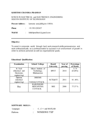
1. KSHITISH CHANDRA PRADHAN
B.TECH IN ELECTRICAL and ELECTRONICS ENGINEERING
SILICON INSTITUTE OF TECHNOLOGY
Present Address : katwaria sarai,delhi,pin-110016.
Phone : +91 9911203437
Mail Id : khitishpradhan1@gmail.com
Objective:
To excel in corporate world through hard work,research,skills,perseverance and
work enthusiastically as a professionalist to succeed in an environment of growth in
order to achieve personal as well as organizational goals.
Educational Qualification:
Examination School/ College Board/
University
Year of
passing
Percentage
of Marks
B. Tech
(Electrical and
Electronics
engineering)
Silicon Institute of
Technology,
Bhubaneswar
BPUT 2014
7.7 4
(CGPA)
Diploma
(electrical
engineering)
DRIEMS
TANGI,CUTTACK
SCTE&VT 2011 81 .46%
Hsc
RAJKISHORE
BIDYAPITHA
CUTTACK
BSE 2008 77.37 %
SOFTWARE SKILLS :
Languages : C , C++ and MATLAB
Platforms : WINDOWS 7/XP
2. B.TECH ACADEMIC PROJECT
Title: Fault location in a long distance transmission line using Artificial Intelligence
(AI) technique.
Objective: To design a 400 kV doubly fed transmission line model and to introduce
different faults in the line so as to study them and fast up the restoration process.
Methodology: Circuit design and implementation is done using MATLAB.
Personal Information:
1. Father’s Name : Dhruba Charan Pradhan
2. Date of Birth : 23h May,1993
3. Gender : Male
4. Nationality : Indian
5. Conversant in : Odiya, Hindi ,English,French
6. Permanent Address : C/o – Dhruba charan pradhan
At- Jagatpur,barrage colony Post- Nimpur
Dist- Cuttack,
State-Odisha
PIN - 754021
Declaration:
I hereby declare that all the above furnished information is true to the best of my knowledge.
Date : 07-06-2015
Place : delhi [Kshitish Chandra Pradhan]
![B.TECH ACADEMIC PROJECT
Title: Fault location in a long distance transmission line using Artificial Intelligence
(AI) technique.
Objective: To design a 400 kV doubly fed transmission line model and to introduce
different faults in the line so as to study them and fast up the restoration process.
Methodology: Circuit design and implementation is done using MATLAB.
Personal Information:
1. Father’s Name : Dhruba Charan Pradhan
2. Date of Birth : 23h May,1993
3. Gender : Male
4. Nationality : Indian
5. Conversant in : Odiya, Hindi ,English,French
6. Permanent Address : C/o – Dhruba charan pradhan
At- Jagatpur,barrage colony Post- Nimpur
Dist- Cuttack,
State-Odisha
PIN - 754021
Declaration:
I hereby declare that all the above furnished information is true to the best of my knowledge.
Date : 07-06-2015
Place : delhi [Kshitish Chandra Pradhan]](data:image/gif;base64,R0lGODlhAQABAIAAAAAAAP///yH5BAEAAAAALAAAAAABAAEAAAIBRAA7)